
 Open Access Article
 This Open Access Article is licensed under a
 Creative Commons Attribution 3.0 Unported Licence
Self-assembly morphology of block copolymers in sub-10 nm topographical guiding patterns†
S.
Gottlieb
 a,
B.
Rösner
b,
L.
Evangelio
a,
M.
Fernández-Regúlez
a,
A.
Nogales
c,
M. C.
García-Gutiérrez
c,
T. F.
Keller
de,
J.
Fraxedas
f,
T. A.
Ezquerra
c,
C.
David
b and
F.
Perez-Murano
*a
a,
B.
Rösner
b,
L.
Evangelio
a,
M.
Fernández-Regúlez
a,
A.
Nogales
c,
M. C.
García-Gutiérrez
c,
T. F.
Keller
de,
J.
Fraxedas
f,
T. A.
Ezquerra
c,
C.
David
b and
F.
Perez-Murano
*a
aInstituto de Microelectrónica de Barcelona IMB-CNM, CSIC, 08193 Bellaterra, Barcelona, Spain. E-mail: Francesc.Perez@csic.es
bLaboratory for Micro- and Nanotechnology, Paul Scherrer Institut, 5232 Villigen-PSI, Switzerland
cInstituto de Estructura de la Materia IEM-CSIC, 28006 Madrid, Spain
dDeutsches Elektronen-Synchrotron DESY, 22607 Hamburg, Germany
eFachbereich Physik, Universität Hamburg, 22607 Hamburg, Germany
fCatalan Institute of Nanoscience and Nanotechnology (ICN2), CSIC and BIST, Campus UAB, Bellaterra, Barcelona 08193, Spain
First published on 4th December 2018
Abstract
In this paper, we investigate the directed self-assembly of block copolymers in topographical guiding patterns with feature sizes in the range of the block copolymer half-pitch. In particular, we present the self-assembly of an 11.7 nm half-pitch block copolymer in sub-10 nm resolution guiding patterns fabricated by the direct e-beam exposure of hydrogen silsesquioxane (HSQ). One result of this analysis is that the block copolymer self-assembles such that the guiding pattern features form part of the 3-D architecture of the film. We are capable of determining a shift in the block copolymer pitch as a function of the guiding pattern pitch with sub-nanometer accuracy by means of both real-space (AFM, SEM) and reciprocal-space techniques (GISAXS). An interesting result is that the block copolymer self-assembly in the studied structures depends on the guiding pattern pitch rather than on the trench width as in standard graphoepitaxy. We analyze the structures by means of a free energy model and present both theoretical and experimental evidence of a narrower processing window for such kind of guiding patterns than for regular directed self-assembly using wide topographical guiding patterns, and discuss the origin of this effect. We argue that chain deformation in the vicinity of the top cap of the guiding pattern feature is responsible for an increase of the free energy of the ordered state, which leads to a smaller energy difference between the defect-free and defective self-assembly than that for the observed self-assembly morphology.
Design, System, ApplicationBlock copolymer lithography has, in the recent years, evolved as a versatile method to pattern surfaces with a resolution from a few tens of nanometers down to a few nanometers. Due to this potential, the technique is at the prospect of gaining importance in semiconductor high-volume manufacturing for sub-10 nm nodes. Currently, the major drawback of block copolymer lithography is the too high defect density as compared with standard lithography techniques. Here, we explore the behaviour of block copolymer self-assembly in topographical guiding patterns with sub-10 nm feature width. We analyse the system with SEM, AFM and GISAXS and reconstruct the molecular structure, i.e. the self-assembly morphology of the block copolymers, based on our measurements and define design rules for such high-resolution guiding patterns. We use a free-energy model to determine the process window for guiding pattern fabrication using the example of an 11.7 nm half-pitch lamellar PS-b-PMMA block copolymer. This work provides new insight into the behaviour of block copolymers during directed self-assembly in topographical guiding patterns with feature widths as small as the characteristic block copolymer domain size. |
Introduction
The directed self-assembly (DSA) of block copolymers (BCPs) has emerged as a nanopatterning technique with a resolution between a few nanometers and a few tens of nanometers.1–6 For this reason, the technique belongs to the group of next-generation lithography (NGL) techniques under consideration for high-volume manufacturing in the microelectronics industry for sub-10 nm feature widths as defined by the International Technology Roadmap for Semiconductors ITRS.7Block copolymers consist of two chemically different polymer chains connected by a covalent bond.8 Upon heating the material above its glass transition temperature, it self-assembles into an ordered phase of well-defined structures. Block copolymers exhibit a complex phase behavior and as a function of the relative and absolute chain lengths, they are capable of assembling into diverse morphologies, like spherical, cylindrical, gyroid or lamellar structures.9–12 Due to large defect-annihilation energies, a self-assembled film of block copolymers will never be free of point defects.13 Lithographically defined structures used to introduce long-range order into self-assembled block copolymers, i.e. to direct the self-assembly of block copolymers, are referred to as guiding patterns. The most frequently used strategies to direct the self-assembly of block copolymers are the fabrication of chemical patterns, referred to as chemoepitaxy,2,14–17 and the fabrication of topographical patterns, referred to as graphoepitaxy.5,18–21
The fabrication of chemical guiding patterns requires patterning techniques with excellent resolution because the chemically modified areas need to be in the size range of the block copolymer domains.15,17 Works concentrating on very high-resolution topographical guiding patterns for lamellar block copolymers are sparse.4 This may be because one of the principal advantages of the use of graphoepitaxy5 is the lower required resolution for the guiding pattern fabrication. High-resolution topographic guiding patterns have been used to direct the self-assembly of a spherical PS-b-PDMS block copolymer by fabricating HSQ posts subsequently covered with a PDMS brush.22 In this case, the authors proposed a free energy model to explain the orientation of the block copolymer template with respect to the guiding pattern as a function of the guiding pattern pitch.
The investigation of the behavior of block copolymers in high-resolution topographical guiding patterns is of technological interest for at least two reasons. On one hand, the need for high-resolution topographical guiding patterns will increase substantially as soon as new high-χ block copolymers or other self-assembling materials with significantly smaller pitches are developed.23 On the other hand, the space on the chip occupied by guiding pattern features represents non-utilizable space for the fabrication of electronic devices on the chip. Therefore, the use of high-resolution topographical guiding patterns represents a noticeable increase in patterning efficiency with respect to systems using large guiding pattern features.24 To our best knowledge there is no work published yet that analyzes the behavior of block copolymers in topographical guiding patterns whose critical feature size has been pushed below the block copolymer domain size.
In addition to standard real-space nanocharacterization methods like SEM and AFM, we use grazing-incidence small-angle X-ray scattering (GISAXS) as a damage-free, high resolution characterization technique that is frequently used to analyze the nanostructure of polymer films.25
A significant advantage of GISAXS over common real-space techniques is that the relatively large sampling volume permits the investigation of a statistically meaningful area both on the sample surface and below.26 The low incidence angles used in GISAXS (usually few tenths of a degree), however, leads to a significantly elongated beam foot print and requires sufficiently large guiding patterns. In the last years, GISAXS has been used to analyze gratings to determine their basic geometric properties,27,28 but also more advanced parameters like the line-edge-roughness (LER) of nanometric structures.29
Here, we report on the directed self-assembly of a 23.4 nm full-pitch lamellar diblock PS-b-PMMA block copolymer with a low defect density in sub-10 nm resolution topographical guiding patterns fabricated by the direct exposure of hydrogen silsesquioxane (HSQ) to an electron beam. The self-assembly is characterized by means of GISAXS, SEM and AFM measurements and compared to the morphology that is known from the directed self-assembly of block copolymers in wide topographical guiding patterns.5 We apply a free energy model21,30 and compare the fabricated structures with respect to the free energy difference between defect-free self-assembly and the defective self-assembly.
Experimental
The substrates used in the experiments are pieces of 2 × 2 cm2 cleaved from a p-doped silicon <100> oriented wafer (4–40 Ω cm resistance).HSQ deposition, exposure and development
The chip is cleaned in an O2 plasma at 100 W for 20 s. We use flowable oxide FOX 16 by Dow Corning Corporation diluted 1![[thin space (1/6-em)]](https://www.rsc.org/images/entities/char_2009.gif) :6 in methyl isobutyl ketone (MIBK) and spin coat this solution at 1000 rpm for 1 min. This yields a film thickness of 42 nm. The exposure of HSQ by electron beam induces a cross-linking process,31–34 which converts the exposed areas into an SiO2-like amorphous material.
:6 in methyl isobutyl ketone (MIBK) and spin coat this solution at 1000 rpm for 1 min. This yields a film thickness of 42 nm. The exposure of HSQ by electron beam induces a cross-linking process,31–34 which converts the exposed areas into an SiO2-like amorphous material.
The exposure is performed with Vistec EBPG 5000+ tool using a 100 kV electron beam with a beam current of 2 nA. The exposure dose for the fabrication of sub-10 nm lines varies from 7400 μC cm−2 to 8800 μC cm−2 as a function of the pattern pitch, which in this work is between 80 nm and 250 nm. The patterns are 512 μm wide and 10 mm long.
After the exposure the non-cross-linked HSQ is removed in a development step using an alkaline developer (Microposit 351 diluted 1:3 in water) for 5 min. Subsequently the sample is dipped in H2O for one minute and air-dried.
Deposition of neutral brush layer
A neutral brush layer is spun from a 0.25 wt% solution of PS-r-PMMA (58 wt% PS and 42 wt% PMMA at a molecular weight Mbrush = 7.9 kg mol−1 and a polydispersity index PDIbrush = 1.85) dissolved in PGMEA. The spin coating conditions are 4000 rpm for 30 s, leading to a film thickness of 4 nm in free surface. An annealing step at 230 °C for 5 min initiates a grafting process of the random copolymers to the activated silicon surface. The non-grafted brush layer is removed by a PGMEA rinsing step.Deposition and self-assembly of block copolymers
For all the experiments in this work we have used a lamellar PS-b-PMMA diblock copolymer (MPS-b-PMMA = 42.3 kg mol−1; 43 wt% PS, 57 wt% PMMA, PDIBCP = 1.1). The natural pitch in free surface is 23.4 nm. Spin-coating of a 1.8 wt% solution in PGMEA at 2000 rpm yields a 34 nm thick film in free surface. Microphase separation is induced by an annealing step at 230 °C for 10 min.Analysis
The samples are inspected by tapping mode AFM using a Dimension Icon/Nanoscope V by Bruker. The amplitude set-point is 50% of the drive amplitude. The SEM inspection is done with a Zeiss Auriga using the InLens detector. GISAXS measurements, using synchrotron radiation, of representative samples are conducted at the P03 Micro- and Nanofocus X-ray Scattering Beamline at PETRA III in Hamburg, Germany.35 The sample-detector distance is set to L = 5800 mm and the radiation wavelength to λ = 0.107 nm, respectively. The incidence angle of the beam is αi = 0.4°. The detector that has been used for these experiments is a PILATUS 300k pixel detector with a readout time below 3 ms and a pixel size of 172 μm × 172 μm.The estimated uncertainty in lateral size determination according to the procedure proposed by Smilgies36 is 0.3 nm. Here, the most important contribution to the measurement uncertainty originates from the beam divergence, while the contribution of the beam band width and geometric smearing is negligibly.
Results
The work-flow pursued to fabricate the guiding patterns is depicted in the top part of Fig. 1 and compared to wide guiding pattern fabrication work-flow, which is sketched in the bottom part of the same figure. The principal difference between the two work-flows is in the guiding pattern feature width. The work-flow sketched in the top images is characterized by a guiding pattern feature width below 10 nm, which is in the size range of the block copolymer domain. The lower line of images depicts a work-flow using guiding patterns with a feature width significantly above the block copolymer domain width. For both alternatives it is particularly important to deposit a thin 4 nm neutral brush layer (using 0.25 wt% random copolymer dissolved in PGMEA) to inhibit grafting of random copolymers to the guiding pattern walls. Otherwise the self-assembly morphology would no longer be in lamellae parallel to the guiding pattern direction, but rather lamellae perpendicular to the guiding pattern direction.4,21 On the other hand, the difference in guiding pattern feature width results in a fundamentally different self-assembly morphology. This difference is indicated in Fig. 1 and will be further explained in the forthcoming paragraphs.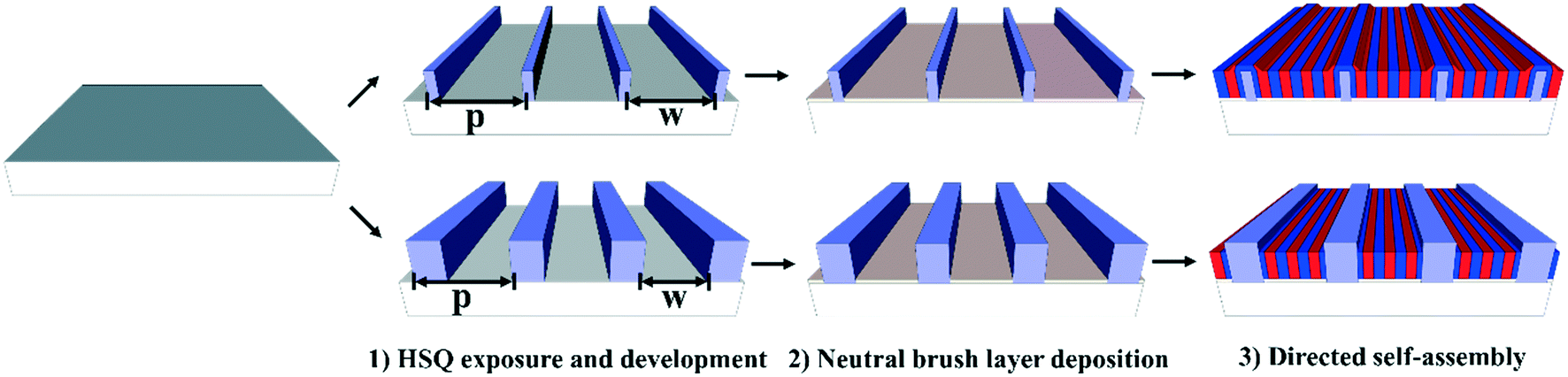 | ||
| Fig. 1 Sketches comparing the self-assembly morphology in topographical guiding patterns with sub-10 nm guiding pattern width (top part) with the self-assembly morphology in guiding patterns with a width significantly above 10 nm (bottom part).The parameter p indicates the guiding pattern pitch, and w the separation between guiding pattern features, so that the guiding pattern width is p–w. | ||
Directed self-assembly characterization by real-space imaging techniques
We analyze results obtained using guiding pattern with sub-10 nm width and nominal pitches of 90 nm, 120 nm and 150 nm, as depicted in the Fig. 2a)–c). The accuracy of the guiding patterns in terms of dimensions (pitch and linewidth) and their low line edge roughness makes them ideal templates for DSA. The SEM images depicted in Fig. 2d)–f) demonstrate their excellent ability to direct the self-assembly of block copolymers. The guiding patterns are capable of directing the self-assembly of block copolymers without the formation of defects over areas of various tens of square micrometers. Here, we define “defects” as deviation from the desired continuous lamella morphology, including point-defects,13 point-like defects21 and domain wiggling.37 The example shown in Fig. 2g) is an SEM image that evidences the defect-free self-assembly in trenches with a 150 nm pitch. The multiplication factor for this pattern is n = 6. This means that the density of the block copolymer features in this pattern is six times larger than the guiding pattern feature density. An advantage of such small guiding pattern features is a significant increase of the area the can be effectively used on the chip, whereas guiding patterns with wide features widths commonly lead to a large proportion of the sample that cannot be used for patterning.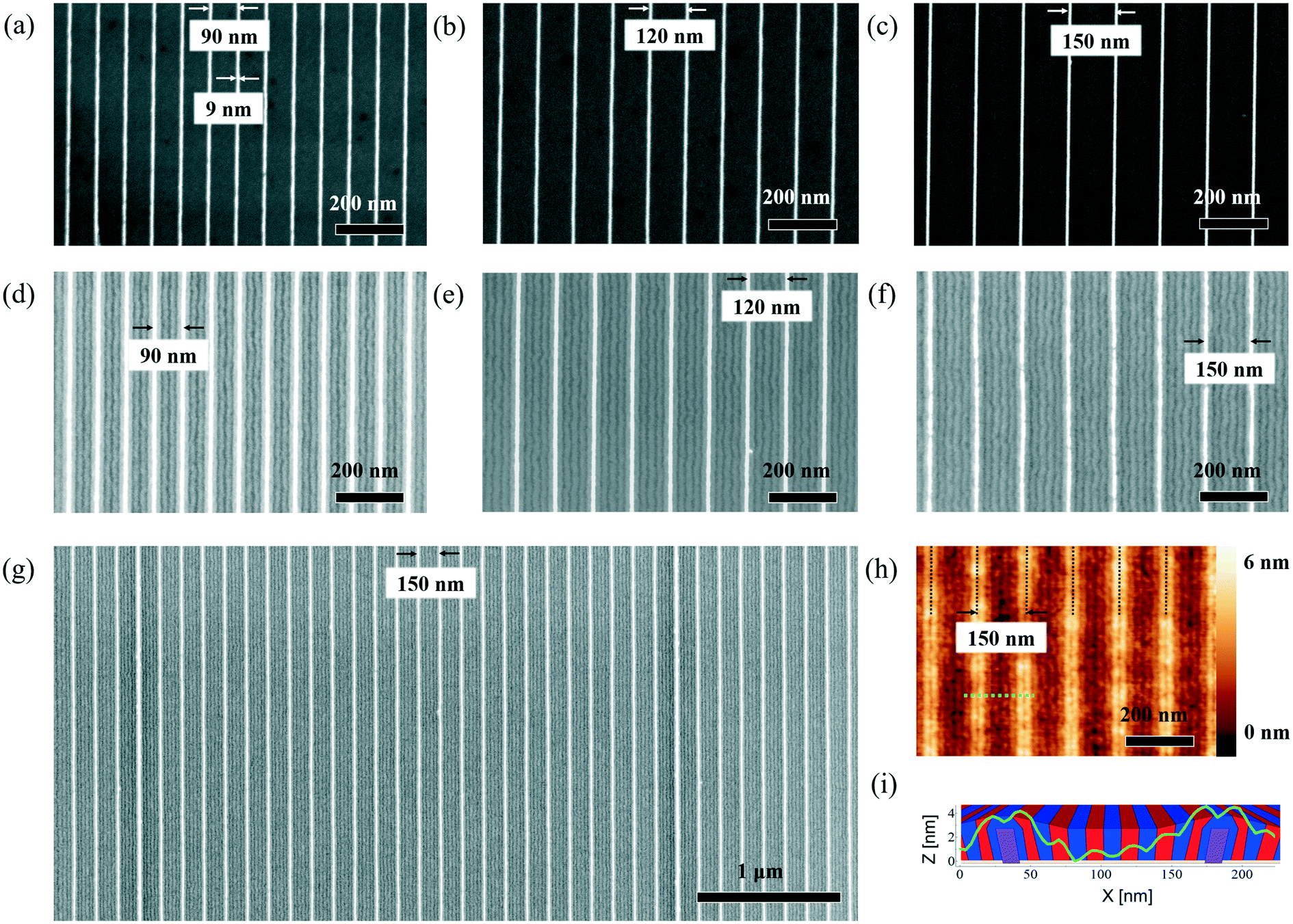 | ||
| Fig. 2 SEM images of patterns with different pitches before and after self-assembly. a)–c): SEM images of 90 nm, 120 nm, 150 nm guiding patterns, d)–f): SEM images of 90 nm, 120 nm, 150 nm guiding patterns with self-assembled block copolymer, g): SEM image of defect-free assembly on large scale, h): AFM height image of the 150 nm structure, i): single line scan along the green dotted line in h) with a sketch of the self-assembly morphology in the background. | ||
Fig. 2h) shows a tapping mode AFM height image of the 150 nm pattern after DSA. Interestingly, we observe that the entire surface is a sequence of PS and PMMA domains, indicating that the guiding pattern features are entirely covered by block copolymer molecules. Based on our observations, we conclude that the block copolymer surrounds the guiding pattern features rather than occupying exclusively the space between them, as it is the case for wide guiding patterns (for a reconstruction of the respective structure, see sketch in Fig. 2i)). A detailed analysis of the AFM image to understand the configuration is shown in the ESI.† A similar self-assembly morphology has been observed in a study analyzing the directed self-assembly of block copolymers based on a chemoepitaxy–graphoepitaxy hybrid process, however, other than in the present study, with only few nanometers of topography.3,38,39
Another interesting observation concerns the different degrees of visibility of the guiding patterns in the AFM height image compared to the SEM image. Although the AFM analysis reveals that the guiding patterns are entirely covered with block copolymers, the guiding pattern lines produce a strong SEM signal. This observation suggests that the block copolymer layer covering the guiding patterns is only few nanometers thick. The coverage of the guiding pattern thus results most likely from an energy minimization process during the self-assembly.
These observations confirm the self-assembly morphology depicted in Fig. 1 and demonstrate that the self-assembly in these patterns differs significantly from the directed self-assembly when the guiding pattern feature width is notably larger than the block copolymer domain.
Analysis of the structures with GISAXS
An important parameter for understanding the behavior of block copolymers under confinement is the strain/compression with respect to their equilibrium spacing L0, which can be determined by measuring the block copolymer pitch. Although we get an excellent qualitative understanding of how the block copolymers self-assemble in our system, it is difficult to determine deviations in the block copolymer pitch with high accuracy by the exclusive use of real-space techniques. Here, we concentrate on the analysis of the block copolymer pitch as a function of the guiding pattern pitch. An analysis of the correlation length can be found in the ESI† part.The geometry of the GISAXS experiment is sketched in Fig. 3a). The samples depicted in Fig. 2a)–f) have been analyzed by GISAXS. The elongated shape of the guiding pattern (512 μm × 10 mm) is necessary to avoid that a large part of the measured signal originates from block copolymers oriented in fingerprint morphology. At the chosen incidence angle of 0.4°, the 50 μm beam has a footprint of slightly more than 7 mm in length, which is shorter than the pattern length and therefore allows us to detect scattered photons originating exclusively from the block copolymer in the guiding pattern.
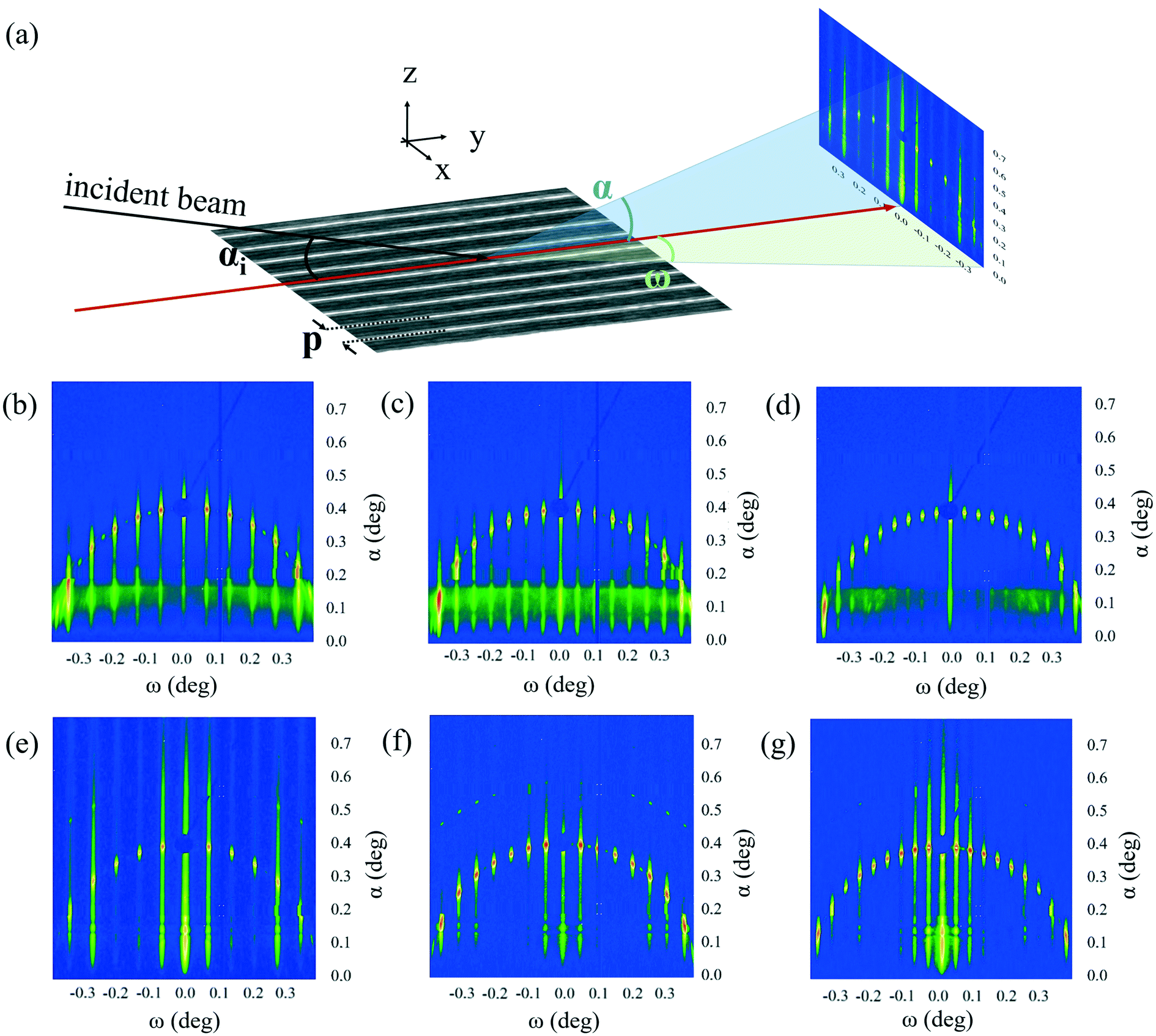 | ||
| Fig. 3 GISAXS analysis of structures with and without block copolymer. a): Geometry of GISAXS experiments, b): GISAXS pattern for 90 nm pitch guiding pattern, c): GISAXS pattern for 120 nm pitch guiding pattern, d): GISAXS pattern for 150 nm pitch guiding pattern, e): GISAXS pattern for 90 nm pitch guiding pattern with self-assembled block copolymer, f): GISAXS pattern for 120 nm pitch guiding pattern with self-assembled block copolymer, g): GISAXS pattern for 150 nm pitch guiding pattern with self-assembled block copolymer. | ||
The GISAXS measurement of the samples with guiding patterns before the deposition of block copolymer shows the characteristic scattering features for such gratings.27 The patterns depicted in Fig. 3b)–d) represent the results of the analysis of the guiding patterns with a nominal pitch of 90 nm, 120 nm and 150 nm. The GISAXS patterns consist of a superposition of the Ewald sphere leading to an arc, and a number of grating truncation rods (GTRs), whose separation indicates the pitch of the real space lattice in reciprocal space.26 We can easily extract the lattice pitch with the Bragg equation, which yields a pitch p1 = 89.9 ± 0.3 nm for Fig. 3b), p2 = 120.3 ± 0.3 nm for Fig. 3c) and p3 = 150.1 ± 0.3 nm for Fig. 3d). These values are mean values of the position of two GTRs in each pattern and demonstrate the excellent precision of the guiding pattern fabrication.
The semicircular shape of the intersection of the Ewald sphere with the detector is very sensitive to the orientation of the pattern with respect to the incident beam.40,41 The nearly perfectly semicircular shape of the arc in the observed pattern suggests a deviation from perfect parallelism of merely few thousandths of a degree. The semicircle has its center in the sample horizon (at α = 0°; ω = 0°) and its radius (in degrees) corresponds to the incidence angle of the beam.28
In Fig. 3e)–g) we depict the scattering patterns of block copolymers after the directed self-assembly. In comparison to the measurements shown before, these patterns show a number of scattering effects in addition to the GTRs and the semicircle we observe in the guiding pattern. These scattering features are consequently due to the self-assembled block copolymer. In general terms, the signal intensity in the patterns decreases notably after the deposition of the block copolymer. The reason for this effect is that the scattering probability at the interface between two materials is proportional to the difference in their electron density. The difference in the electron density between air and SiO2 in case of the guiding pattern sample, is larger than the difference in electron density between the SiO2 and block copolymer. In each GISAXS pattern there is one GTR that stands out of the rest due to its enhanced intensity. For Fig. 3e), the high-intensity GTR corresponds to the 4th order, for Fig. 3f), to the 5th order and for Fig. 3g) to the 6th order GTR. While this effect is important in the GISAXS pattern of the 90 nm grating, it is rather weak in the 120 nm and the 150 nm grating. An important conclusion from this observation is that the order of the GTR that shows this phenomenon corresponds to the multiplication factor n we observed in the SEM and AFM analysis of our structures (Fig. 2). Additional features that distinguish the GISAXS patterns after block copolymer deposition from those before deposition is the existence of satellite arcs that other authors have previously interpreted as a result of line edge roughness in the analyzed pattern but will not be made a further subject of discussion in this paper.42 Finally, we notice an intensity modulation in the range of α = {0.1°; 0.15°} which is related to the different material composition of the sample with block copolymer compared to the one without block copolymer.43
The overall aspect of the GISAXS pattern is similar to those that have been taken from block copolymers directed by chemical guiding patterns.44,45 In these works, the authors also observe the effect of intensity enhancement of the n-th GTR for guiding patterns with a multiplication factor n. The similarity between GISAXS measurements of our patterns and on samples with block copolymer self-assembly directed by chemoepitaxy supports our thesis that (i) the intensification of determined GTRs is due to the presence of block copolymers, (ii) we can draw conclusions about the block copolymer structure based on the position of the intensified GTR and (iii) the topographical guiding pattern actually forms part of the 3D morphology of the block copolymer pattern.
In the following, we will analyze specific transverse cuts through the GISAXS pattern of the 90 nm pitch grating sample before and after the deposition of block copolymers and in particular investigate the origin of the enhanced intensity of the 4th order GTR.
In Fig. 4a) we compare cuts at α = {0.125° ± 0.025} (i.e. around the Yoneda peak43 of the block copolymer materials) of the guiding pattern (red curve), the guiding pattern with block copolymer (black curve) and a block copolymer in free surface (blue curve). Small versions of the respective patterns are depicted in the panel as in-sets and the approximate position of the cut is indicated by the white dotted line. The color of the respective inset frame corresponds to the color of the curve.
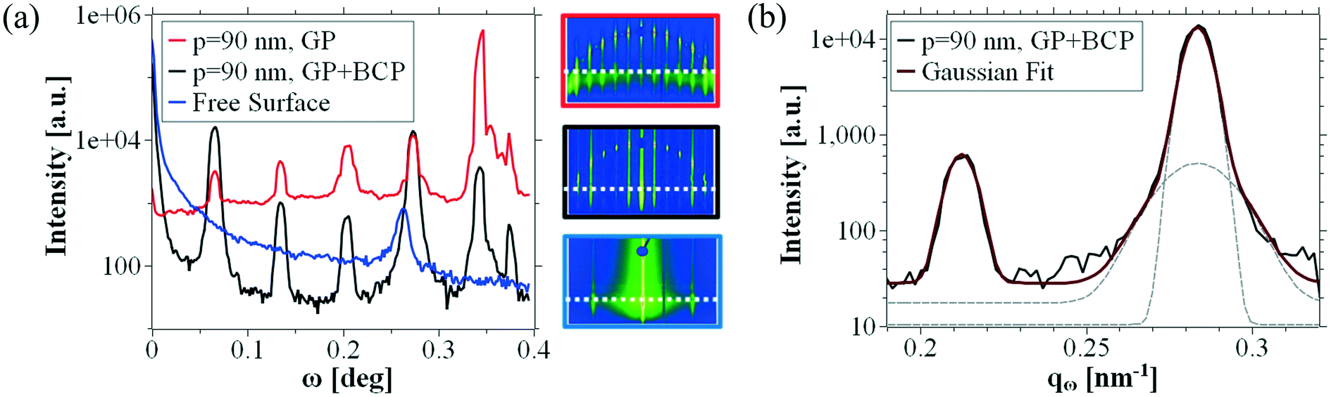 | ||
| Fig. 4 Determination of the block copolymer pitch with sub-nm resolution. a): Cuts through GISAXS patterns depicted on the right at exit angle α = 0.125° ± 0.025° (see white dashed lines) and zoomed into the relevant area, b): 3rd order peak of 90 nm pitch guiding pattern peak and its single-peak fit, and 4th order peak of 90 nm pitch guiding pattern and its double-peak fit. | ||
The GISAXS analysis of the fingerprint pattern sample yields only one peak (ω = 0.267°), that corresponds to the periodicity of the block copolymer pattern. The peak position suggests a natural block copolymer pitch L0 = 23.4 ± 0.3 nm. In addition to that, the block copolymer fingerprint pattern produces a remarkable scattering intensity at small diffraction angles ω, causing a large background intensity in the blue curve.
For the black and the red curve, we observe GTRs at the same diffraction angles ω before and after the block copolymer deposition. The absence of a peak at ω = 0.267° confirms that the amount of illuminated material outside the guiding pattern (e.g. material self-assembled in fingerprint morphology) in this experiment is negligible. Although the overall signal declines after the deposition of the block copolymer, we observe that the black curve has a background intensity whose shape is very similar to the one measured in the fingerprint sample. This phenomenon seems to be an effect caused by block copolymers and results in the misleading impression that low-order GTRs have a significantly higher scattering intensity than the higher-order GTRs. The conversion from scattering angle ω into the q-space is done with Bragg's law using
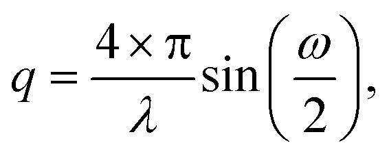 | (1) |
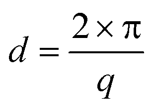 | (2) |
We would like to clarify at this point that the enhanced intensity and the particular shape of the 5th order peak both in the red curve and the black curve in Fig. 4a) originates from the fact that the arc and the 5th order GTR intersect precisely in the integration area of the analyzed cut and is therefore due to a different phenomenon. This concept becomes clear when we look at the in-sets of the GISAXS spectra in Fig. 4a), where the dashed white line represents the area where the cut has been realized. Based on this observation, on the AFM/SEM analysis presented in Fig. 2 and on the similarity of this system to a chemoepitaxy system,44,45 we deduce that this peak represents a superposition of the 4th guiding pattern GTR and the 1st order block copolymer GTR. This implies that the pitch of the block copolymer that is deposited in the 90 nm guiding pattern area differs from its natural pitch L0 = 23.4 nm by approximately 4.2% (corresponding to a pattern compression, such that the new pattern full-pitch is 22.5 nm). The distortion of cylindrical block copolymers due to guiding pattern incommensurability has been observed by GISAXS before for minimal topographical guiding patterns.46
Discussion
So far, it has been consensus that graphoepitaxial guiding patterns have to be designed such that the space between the guiding patterns is exactly or close to an integer multiple of the natural block copolymer pitch.21,30,47,48This rule implies that the successful design of graphoepitaxial guiding patterns depends on the interplay of pattern pitch p and pattern width wGP. Based on the analysis presented in the Results section of this paper, we conclude that the design rule for the successful alignment of block copolymers in topographical guiding patterns with feature sizes in the range of individual block copolymer domains differs fundamentally from those for wide topographical guiding patterns. Similar to chemoepitaxy, the high-resolution topographical guiding patterns have to be designed such that their pitch (and not the space between two guiding pattern features) is in the close vicinity of an integer multiple of the block copolymer pitch (see Fig. 5a)–e)).
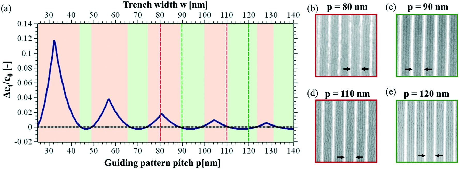 | ||
| Fig. 5 (a) Excess of free energy per block copolymer chain in units of the free energy in unconfined state (eqn (6)). The excess of free energy is calculated as the difference between the free energy of the defective state and the energy of the non-defective state, taking into account the deformation of the block copolymer on top of the guiding pattern. (b)–(d): SEM images on trenches defined by high resolution guiding patterns as a function of guiding pattern pitch, p. Images with a red framework indicate patterns with defects, while the green ones indicate non-defective alignment. | ||
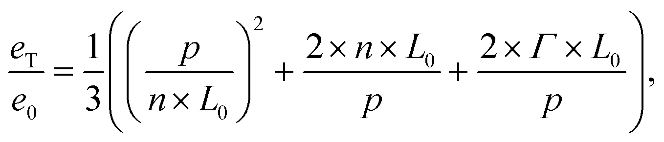
A model to describe the normalized free energy of block copolymers under confinement has been developed by Turner and successfully used to describe the self-assembly of block copolymers in topographical guiding patterns.30,49 We have recently introduced an extension of this model to explain the free energy of a self-assembly morphology with a high defect density as it can also be found in our experiments for strongly incommensurate pitches.21 In the following, we will estimate the free energy of the block copolymers self-assembled in sub-10 nm guiding patterns using a further extension of the previously presented model (Fig. 5a)). The model allows to predict the process window due to variations of the pitch dimensions.
We observe, as a function of the pattern guiding dimensions, alternating regions with successful self-assembly and regions where the self-assembly shows a large number of defects, referred to as defect-loaded state due to incommensurability. The self-assembly in samples with guiding patterns with 80 nm and 110 nm pitch leads to a very large defect density in the block copolymer template (see images in Fig. 5b) and d)), where images with a red frame are examples for self-assembly with a large number of defects and images with a green frame represent examples with a defect-free self-assembly. The guiding patterns with 90 nm and 120 nm pitch do, however, provide a self-assembly morphology that is free of defects (Fig. 5c) and e)). The starting point of the extended model to describe the free energy of laterally confined block copolymers is the model derived by Turner to deduce eT/e0. Here, eT is the free energy of one macromolecule confined in a trench of width w in consideration of the deformation free energy, the polymer–wall interaction and the A/B-interfaces, and e0 corresponds to the free energy per macromolecule under equilibrium conditions. Despite of the differences in pattern feature width, we find that results elaborated for the design of wide guiding patterns are adaptable for the present system if we consider the guiding pattern pitch instead of the trench width as independent variable (note the two different x-axis on top and at the bottom of Fig. 5a)). For this reason, the trench width w from the original equation has been replaced by pattern pitch p to adapt the model to the system corresponding to the present guiding pattern morphology:
 | (3) |
The material dependent Flory–Huggins interaction parameter influences the energy level of the molecule in equilibrium conditions e0. By normalizing the equation with e0, the material dependence of eqn (3) cancels out for its first two summands. The third summand still contains the polymer–wall-interaction energy. This is a material parameter that increases the free energy level of the system, but does not have any influence on the position of characteristic points on the p-axis.
We will now add a summand eD/e0 to this equation, which accounts for the additional free energy introduced into the system due to the distortion of the block copolymer features in the direct vicinity of the top cap of the guiding pattern features, so that the equation turns into:
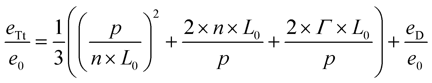 | (4) |
We call the expression eTt/e0 because it describes the free energy of the system in thin guiding patterns. With the summand eD/e0 we account for the free-energy caused by chain deformation in the self-assembled system that is independent of the incommensurability.3
The normalized free energy according to Turner in thin guiding patterns (eqn (4)) is now compared with a term that we call e/e0 and describes the free energy of the system, when it forms defects. This term sums up the normalized free energy in free surface (i.e. 1), the interface free energy contribution due to the interaction between the block copolymers and guiding pattern features (i.e. 2 × Γ × L0/3 × p) and a constant energy penalty term accounting for an additional free energy contribution (including, for example, the formation of additional interfaces, domain wiggling and chain stretching) called ep/e0
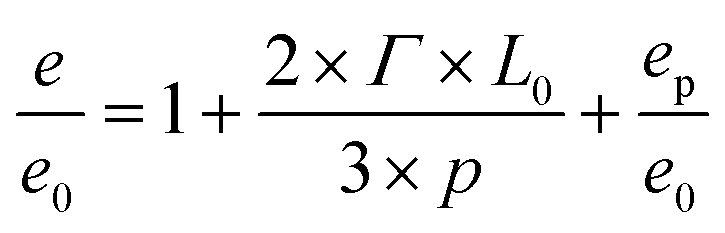 | (5) |
Following the reasoning presented in a previous work,21 we can state that the system forms defects, if the term Δet/e0 defined as
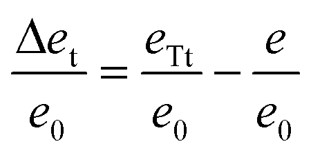 | (6) |
We determine a distortion parameter that we call eD. The determination of eD is based on the assumption that the penalty term ep (previously estimated at 0.007 for the self-assembly of PS-b-PMMA in wide guiding patterns21) is valid for all the macromolecules in this system that are not subjected to distortion in the close vicinity of the top cap of the guiding pattern features, as argued in the Results section. To describe our new system accurately, we introduce the distortion term, which effectively increases the free energy of the defect-free state due to the deformation of molecules close to the top cap of the guiding pattern features. The term eD is not a function of the guiding pattern pitch, because the said distortion is independent of the (in-)commensurability of the guiding patterns. In that sense, this parameter depends on the difference between the width of the guiding pattern feature and the width of the domain of the preferentially wetting block (here PMMA). According to our understanding, the domain distortions in the vicinity of the top cap of the guiding pattern features would reach a minimum in case the two had the same size. Based on this, we state that the parameter eD is the reason for the observed narrowing of the process window and estimate
| eD ≈ 0.003 e0 | (7) |
We provide a detailed derivation of the model including the distortion parameter eD in the ESI† part. For our particular case we derive that part of eD is due to the fact that the guiding pattern features are smaller than the wetting PMMA domain, and the PMMA domain is subjected to compressive force. This structural change can neither be directly observed in the GISAXS nor in the AFM measurements. Using the equation proposed by Ohta and Kawasaki,51 we can now estimate that the energy penalty due to the domain distortion in the close vicinity of the guiding pattern features accounts for about nine thousandths of kT per chain. This free energy component does not exist in the self-assembly of block copolymers in wide guiding patterns. Our interpretation of this term is that eD represents the reason for the smaller process window for the successful alignment of block copolymers in thin topographical guiding patterns than in wide topographical guiding patterns. The smaller process window is particularly obvious when we compare the 110 nm pitch thin feature guiding pattern with the 110 nm trench width pattern for wide guiding pattern features.21 While the wide guiding pattern shows defect-free assembly, the thin 110 nm pitch guiding pattern is clearly inside the defective area for the high-resolution guiding patterns. An investigation of the maximum guiding pattern width able to produce the self-assembly morphology presented here would provide information about the tolerance of the guiding pattern dimensions.
The continuity of the block copolymer film on top of the guiding pattern (which is the prerequisite both for the particular block copolymer self-assembly and the successful GISAXS analysis) is certainly only observed in samples where the amount of deposited block copolymer is sufficiently large. In a situation where a significantly lower block copolymer thickness is deposited or the guiding pattern features would have been significantly higher, it is conceivable that the block copolymer self-assembles in a discontinuous fashion as usually observed in wide-guiding pattern feature graphoepitaxy.
This finding, furthermore, demonstrates that the maximum free energy difference between the ordered (i.e. defect-free) and the disordered (i.e. defect-loaded) state in the described system merely accounts for 0.004 e0, which is a result that is in good agreement with calculations done by Garner et al. for chemical guiding patterns.52 The maximum free energy difference is here defined as the free energy difference for completely commensurate topographical thin guiding patterns. As the distortions only occur close to the top cap of the features, structural fluctuations only occur in a small part of the pattern and a reliable pattern transfer may therefore still be possible.3,38
Conclusions
We have presented the fabrication of topographical guiding patterns for the directed self-assembly of block copolymers with sub-10 nm resolution by electron beam exposure of HSQ. During the self-assembly in these guiding patterns, we observe a self-assembly morphology, where the block copolymer self-assembles not only between the guiding pattern features, but also on top of them. We deduce that the prerequisite for the block copolymer to self-assemble in this morphology is that the guiding pattern features are in the size range of the PMMA domain of the block copolymer.We demonstrate that free energy models describing the self-assembly in wide guiding patterns are still valid for the description of our system after minor adjustments are introduced. Based on the modified model and the experimental results of this work, we determine that the maximum difference between the defect-free and the defect-loaded state for thin guiding pattern features is generally only about half as large as for the directed self-assembly in wide guiding patterns. We report that this is due to the distortion created by the incorporation of the thin guiding pattern features in the block copolymer thin film. As a result, the process window for the guiding pattern fabrication is smaller than for regular wide topographical guiding patterns. However, our results indicate that the fabrication of efficient, high resolution guiding patterns is durable despite the reduced process window, which could be relevant to the upcoming of high-chi (low pitch) block copolymers.
The present structures have been analyzed by AFM, SEM and GISAXS. Detailed peak-analysis of GISAXS measurements reinforce the thesis about the morphology derived from the characterization performed by real-space imaging techniques. Furthermore, GISAXS enables the determination of the changing block copolymer pitch as a function of the guiding pattern pitch with sub-nm resolution. We furthermore propose a method to qualitatively analyze the defect density of block copolymers in narrow topographical guiding patterns by GISAXS.
Conflicts of interest
There are no conflicts of interest to declare.Acknowledgements
This project is partially funded by the EU project NFFA (Nanoscience Foundries and Fine Analysis) (grant agreement no. 654360) and by MICINN through the Nanointegra project (TEC2015-69864-R). The ICN2 is funded by the CERCA program/Generalitat de Catalunya. The ICN2 is supported by the Severo Ochoa program of MICINN (SEV-2013-0295). We would like to acknowledge Christophe Navarro and Celia Nicolet from Arkema for supplying some of the polymers used in this work. We would, furthermore, like to acknowledge the team, in particular Dr. Björn Beyersdorff, of the P03 Micro- and Nanofocus X-ray Scattering Beamline at PETRA III in Hamburg, Germany, and thank them for the technical support during our GISAXS measurements.References
- S. O. Kim, H. H. Solak, M. P. Stoykovich, N. J. Ferrier, J. J. De Pablo and P. F. Nealey, Nature, 2003, 424, 411–414 CrossRef CAS PubMed.
- R. Ruiz, H. Kang, F. A. Detcheverry, E. Dobisz, D. S. Kercher, T. R. Albrecht, J. J. de Pablo and P. F. Nealey, Science, 2008, 321, 936–939 CrossRef CAS PubMed.
- G. Blachut, S. M. Sirard, M. J. Maher, Y. Asano, Y. Someya, A. P. Lane, W. J. Durand, C. M. Bates, A. M. Dinhobl, R. Gronheid, D. Hymes, C. J. Ellison and C. G. Willson, Chem. Mater., 2016, 28, 8951–8961 CrossRef CAS.
- A. P. Lane, X. Yang, M. J. Maher, G. Blachut, Y. Asano, Y. Someya, A. Mallavarapu, S. M. Sirard, C. J. Ellison and C. G. Willson, ACS Nano, 2017, 11, 7656–7665 CrossRef CAS PubMed.
- B. R. A. Segalman, H. Yokoyama and E. J. Kramer, Adv. Mater., 2001, 13, 1152–1155 CrossRef.
- W. Li and M. Müller, Prog. Polym. Sci., 2016, 54–55, 47–75 CrossRef CAS.
- M. Neisser and S. Wurm, Adv. Opt. Technol., 2015, 4, 235–240 Search PubMed.
- F. S. Bates and G. H. Fredrickson, Phys. Today, 1999, 52, 32–38 CrossRef CAS.
- A. Knoll, A. Horvat, K. S. Lyakhova, G. Krausch, G. J. A. Sevink, A. V. Zvelindovsky and R. Magerle, Phys. Rev. Lett., 2002, 89, 1–4 CrossRef PubMed.
- L. Leibler, Macromolecules, 1980, 13, 1602–1617 CrossRef CAS.
- M. P. Stoykovich, E. W. Edwards, H. H. Solak and P. F. Nealey, Phys. Rev. Lett., 2006, 97, 4–7 CrossRef PubMed.
- M. W. Matsen and F. S. Bates, Macromolecules, 1996, 29, 1091–1098 CrossRef CAS.
- W. Li and M. Müller, Annu. Rev. Chem. Biomol. Eng., 2015, 6, 187–216 CrossRef CAS PubMed.
- S. Ji, L. Wan, C. Liu and P. F. Nealey, Prog. Polym. Sci., 2016, 54–55, 76–127 CrossRef CAS.
- S. Gottlieb, M. Lorenzoni, L. Evangelio, M. Fernández-Regúlez, Y. K. Ryu, C. Rawlings, M. Spieser, A. W. Knoll and F. Perez-Murano, Nanotechnology, 2017, 28, 1–9 Search PubMed.
- C. C. Liu, E. Han, M. S. Onses, C. J. Thode, S. Ji, P. Gopalan and P. F. Nealey, Macromolecules, 2011, 44, 1876–1885 CrossRef CAS.
- M. Fernández-Regúlez, L. Evangelio, M. Lorenzoni, J. Fraxedas and F. Perez-Murano, ACS Appl. Mater. Interfaces, 2014, 6, 21596–21602 CrossRef PubMed.
- D. Borah, M. T. Shaw, J. D. Holmes and M. A. Morris, ACS Appl. Mater. Interfaces, 2013, 5, 2004–2012 CrossRef CAS PubMed.
- D. Borah, S. Rassapa, M. T. Shaw, R. G. Hobbs, N. Petkov, M. Schmidt, J. D. Holmes and M. Morris, J. Mater. Chem. C, 2013, 1, 1192–1196 RSC.
- R. Tiron, X. Chevalier, C. Couderc, J. Pradelles, J. Bustos, L. Pain, G. Fleury and G. Hadziioannou, J. Vac. Sci. Technol., B: Nanotechnol. Microelectron.: Mater., Process., Meas., Phenom., 2011, 29, 1–8 Search PubMed.
- S. Gottlieb, D. Kazazis, I. Mochi, L. Evangelio, M. Fernández-Regúlez, Y. Ekinci and F. Perez-Murano, Soft Matter, 2018, 14, 6799–6808 RSC.
- I. Bita, J. K. W. Yang, S. J. Yeon, C. A. Ross, E. L. Thomas and K. K. Berggren, Science, 2008, 321, 939–943 CrossRef CAS PubMed.
- K. Nickmans, J. N. Murphy, B. De Waal, P. Leclère, J. Doise, R. Gronheid, D. J. Broer and A. P. H. J. Schenning, Adv. Mater., 2016, 28, 10068–10072 CrossRef CAS PubMed.
- S. Jeong, J. E. Kim, H. Moon, B. H. Kim, S. M. Kim, J. B. Kim and S. O. Kim, Nano Lett., 2009, 9(6), 2300–2305 CrossRef CAS PubMed.
- P. Müller-Buschbaum, J. S. Gutmann, R. Cubitt and W. Petry, Phys. Rev. B: Condens. Matter Mater. Phys., 2004, 350, 207–210 CrossRef.
- M. Pflügler, V. Soltwisch, J. Probst, F. Scholze and M. Krumrey, IUCrJ, 2017, 4, 1–8 CrossRef PubMed.
- J. Wernecke, F. Scholze and M. Krumrey, Rev. Sci. Instrum., 2012, 83, 1039061–1039068 CrossRef PubMed.
- D. R. Rueda, I. Martín-Fabiani, M. Soccio, N. Alayo, F. Pérez-Murano, E. Rebollar, M. C. García-Gutiérrez, M. Castillejo and T. A. Ezquerra, J. Appl. Crystallogr., 2012, 45, 1038–1045 CrossRef CAS.
- H. S. Suh, X. Chen, P. A. Rincon-Delgadillo, Z. Jiang, J. Strzalka, J. Wang, W. Chen, R. Gronheid, J. J. De Pablo, N. Ferrier, M. Doxastakis and P. F. Nealey, J. Appl. Crystallogr., 2016, 49, 823–834 CrossRef CAS.
- M. S. Turner, Phys. Rev. Lett., 1992, 69, 1788–1791 CrossRef CAS PubMed.
- A. E. Grigorescu and C. W. Hagen, Nanotechnology, 2009, 292001, 1–31 Search PubMed.
- Z. Min, C. Baoqin, X. Changqing, L. Ming and N. Jiebing, Proc. 2010 5th IEEE Conf. Nano/Micro Eng. Mol. Syst., 2010, vol. 5592584, pp. 1021–1024 Search PubMed.
- A. G. Caster, S. Kowarik, A. M. Schwartzberg, O. Nicolet, S. Lim and S. R. Leone, J. Raman Spectrosc., 2009, 40, 770–774 CrossRef CAS.
- W. Henschel, Y. M. Georgiev and H. Kurz, J. Vac. Sci. Technol., B: Microelectron. Nanometer Struct.--Process., Meas., Phenom., 2003, 21, 2018–2025 CrossRef CAS.
- A. Buffet, A. Rothkirch, R. Döhrmann, V. Körstgens, M. M. Abul Kashem, J. Perlich, G. Herzog, M. Schwartzkopf, R. Gehrke, P. Müller-Buschbaum and S. V. Roth, J. Synchrotron Radiat., 2012, 19, 647–653 CrossRef CAS PubMed.
- D. M. Smilgies, J. Appl. Crystallogr., 2009, 42, 1030–1034 CrossRef CAS PubMed.
- Z.-G. G. Wang, J. Chem. Phys., 1994, 100, 2298–2309 CrossRef CAS.
- T. Segal-Peretz, J. Ren, S. Xiong, G. Khaira, A. Bowen, L. E. Ocola, R. Divan, M. Doxastakis, N. J. Ferrier, J. De Pablo and P. F. Nealey, ACS Nano, 2017, 11, 1307–1319 CrossRef CAS PubMed.
- A. F. Hannon, D. F. Sunday, A. Bowen, G. Khaira, J. Ren, P. F. Nealey, J. J. De Pablo and R. J. Kline, Mol. Syst. Des. Eng., 2018, 3, 376–389 RSC.
- M. Tolan, W. Press, F. Brinko and J. P. Kotthaus, Phys. Rev. B: Condens. Matter Mater. Phys., 1995, 51, 2239–2251 CrossRef CAS.
- M. Jergel, T. Baumbach, E. Majkov and E. Piň, J. Phys. D: Appl. Phys., 2001, 34, A188–A192 CrossRef.
- A. Kato, S. Burger and F. Scholze, Appl. Opt., 2012, 51, 6457–6464 CrossRef PubMed.
- Y. Yoneda, Phys. Rev., 1963, 131, 2010–2013 CrossRef.
- J. Wernecke, M. Krumrey, A. Hoell, R. J. Kline, H. K. Liu and W. L. Wu, J. Appl. Crystallogr., 2014, 47, 1912–1920 CrossRef CAS.
- J. Y. Cheng, D. P. Sanders, H. D. Truong, S. Harrer, A. Friz, S. Holmes, M. Colburn and W. D. Hinsberg, ACS Nano, 2010, 4, 4815–4823 CrossRef CAS PubMed.
- J. Choi, I. Gunkel, Y. Li, Z. Sun, F. Liu, H. Kim, K. R. Carter and T. P. Russell, Nanoscale, 2017, 9, 14888–14896 RSC.
- D. Walton, G. J. Kellogg, A. Mayes, P. Lambooy and T. P. Russell, Macromolecules, 1994, 27, 6225–6228 CrossRef CAS.
- H. Tsai, H. Miyazoe, J. Cheng, M. Brink, S. Dawes, D. Klaus, J. Bucchignano, D. Sanders, E. Joseph, M. Colburn and M. Guillorn, Proc. SPIE, 2015, 942314, 14 Search PubMed.
- I. Keen, H. Cheng, A. Yu, K. S. Jack, T. R. Younkin, M. J. Leeson, A. K. Whittaker and I. Blakey, Macromolecules, 2014, 47, 276–283 CrossRef CAS.
- M. Maret, R. Tiron, X. Chevalier, P. Gergaud, A. Gharbi, C. Lapeyre, J. Pradelles, V. Jousseaume, G. Fleury, G. Hadziioannou, N. Boudet and C. Navarro, Macromolecules, 2014, 47, 7221–7229 CrossRef CAS.
- T. Ohta and K. Kawasaki, Macromolecules, 1986, 19, 2621–2632 CrossRef CAS.
- G. P. Garner, P. Rincon Delgadillo, R. Gronheid, P. F. Nealey and J. J. De Pablo, Mol. Syst. Des. Eng., 2017, 2, 567–580 RSC.
Footnote |
| † Electronic supplementary information (ESI) available. See DOI: 10.1039/c8me00046h |
| This journal is © The Royal Society of Chemistry 2019 |