 Open Access Article
 This Open Access Article is licensed under a Creative Commons Attribution-Non Commercial 3.0 Unported Licence
Spectroscopic elucidation of ionic motion processes in tunnel oxide-based memristive devices
Christoph
Baeumer
 a,
Thomas
Heisig
a,
Benedikt
Arndt
a,
Katharina
Skaja
a,
Francesco
Borgatti
b,
Francesco
Offi
c,
Federico
Motti
d,
Giancarlo
Panaccione
e,
Rainer
Waser
af,
Stephan
Menzel
a and
Regina
Dittmann
*a
a,
Thomas
Heisig
a,
Benedikt
Arndt
a,
Katharina
Skaja
a,
Francesco
Borgatti
b,
Francesco
Offi
c,
Federico
Motti
d,
Giancarlo
Panaccione
e,
Rainer
Waser
af,
Stephan
Menzel
a and
Regina
Dittmann
*a
aPeter Gruenberg Institute 7, Forschungszentrum Juelich GmbH, JARA-FIT, 52425 Juelich, Germany. E-mail: r.dittmann@fz-juelich.de
bCNR, Istituto per lo Studio dei Materiali Nanostrutturati (ISMN), Via P. Gobetti 101, 40129 Bologna, Italy
cCNISM, Dipartimento di Scienze, Università di Roma Tre, Via della Vasca Navale 84, 00146, Rome, Italy
dDipartimento di Fisica, Università di Milano, Via Celoria 16, I-20133 Milano, Italy
eIstituto Officina dei Materiali (IOM)-CNR, Laboratorio TASC, in Area Science Park, 34149 Trieste, Italy
fInstitute of Materials in Electrical Engineering and Information Technology, RWTH Aachen University, 52056 Aachen, Germany
First published on 3rd September 2018
Abstract
Resistive switching oxides are highly attractive candidates to emulate synaptic behaviour in artificial neural networks. Whilst the most widely employed systems exhibit filamentary resistive switching, interface-type switching systems based on a tunable tunnel barrier are of increasing interest, since their gradual SET and RESET processes provide an analogue-type of switching required to take over synaptic functionality. Interface-type switching devices often consist of bilayers of one highly mixed-conductive oxide layer and one highly insulating tunnel oxide layer. However, most tunnel oxides used for interface-type switching are also prone to form conducting filaments above a certain voltage bias threshold. We investigated two different tunnel oxide devices, namely, Pr1−xCaxMnO3 (PCMO) with yttria-stabilized ZrO2 (YSZ) tunnel barrier and substoichiometric TaOx with HfO2 tunnel barrier by interface-sensitive, hard X-ray photoelectron spectroscopy (HAXPES) in order to gain insights into the chemical changes during filamentary and interface-type switching. The measurements suggest an exchange of oxygen ions between the mixed conducting oxide layer and the tunnel barrier, that causes an electrostatic modulation of the effective height of the tunnel barrier, as the underlying switching mechanism for the interface-type switching. Moreover, we observe by in operando HAXPES analysis that this field-driven ionic motion across the whole area is sustained even if a filament is formed in the tunnel barrier and the device is transformed into a filamentary-type switching mode.
1. Introduction
Memristive devices based on resistively switching transition metal oxides are highly attractive candidates for future energy-efficient non-volatile memory1,2 such as storage class memory. Furthermore, a steep increase has arisen in research on memristive devices for the emulation of synaptic functionality in artificial neural networks. Whilst the most widely employed oxide systems exhibit filamentary resistive switching, interface-type switching systems3,4 based on a tunable tunnel barrier are of increasing interest since they suffer less from the variability induced by the stochastic filament formation process. Moreover, in contrast to filamentary systems, which exhibit a sharp SET process caused by the self-accelerating filament formation, interface-type switching devices show gradual switching for both SET and RESET, providing an analogue-type of switching for both polarities as required to adopt synaptic functionality.Interface-type switching devices usually consist of bilayers of one highly mixed-conductive oxide layer and one highly insulating tunnel oxide layer. It is commonly supposed that resistive switching in these devices is induced by a laterally homogeneous change in the tunnel barrier height induced by the field-driven motion of oxygen ions. However, the details of the underlying processes are not well understood so far. The scenario is further complicated by the fact that most tunnel oxides used for interface-type switching are also prone to form conducting filaments above a certain voltage bias threshold.5 Here, we investigated two different tunnel oxide devices, namely, Pr1−xCaxMnO3 (PCMO) with yttria-stabilized ZrO2 (YSZ) tunnel barrier and substoichiometric TaOx with HfO2 tunnel barrier, by hard X-ray photoelectron spectroscopy (HAXPES), in order to gain insights about the chemical changes in different heterostructures during filamentary and interface-type switching.
Thanks to the larger probing depth (>10 nm) achievable with respect to conventional, soft X-ray photoelectron spectroscopy, HAXPES provides an excellent, nondestructive approach to probe chemical changes and charging effects of interfaces buried inside layered heterostructures, in addition to the bulk electronic structure of the materials.6–14 In particular, in operando HAXPES provides an opportunity to correlate the resistive switching effects to the electronic structure and the electrical potential of the probed volume.15–17
For the PCMO/YSZ heterostructures, we observed a reversible shift of the Zr 3d core-level between the two resistive states during interface-type switching, which we attribute to a shift of negative charge into the YSZ layer during the RESET process.16 This is consistent with an exchange of oxygen ions between PCMO and YSZ that causes an electrostatic modulation of the effective height of the YSZ tunnel barrier. For this material stack, the devices show a permanent breakdown when a certain bias value is exceeded and no filamentary switching mode can be stabilized.
For interface-type switching TaOx/HfO2 heterostructures, we were able to also turn the devices into a filamentary switching mode with the same switching polarity. We recorded the Ta and Hf core-level peaks after the application of positive and negative bias, respectively, by in operando HAXPES. The observed shifts of the Hf and Ta core-level spectra and the varying amounts of substoichiometric TaOx are consistent with a reversible shift of oxygen vacancies between the TaOx layer and the HfO2 layer during filamentary switching. However, due to the comparably small estimated filament size, the relative change of the electronic structure would be insufficient in order to be detected on the large device area of 60 × 200 μm2. We therefore attribute our observations to changes of the electronic structure across the whole device area taking place as a side effect during electrical biasing. We could thereby evidence a co-existence of strongly temperature-accelerated ionic motion within the filament and near room temperature ionic motion taking place over the whole device area. We complemented our measurements with finite-element calculations of the field and temperature distribution in our devices and discuss its implications on the co-existence of the two processes.
2. PCMO/YSZ layer stacks
2.1. Resistive switching properties
The first resistively switching layer stack chosen for our studies was a YSZ/PCMO layer stack epitaxially grown by pulsed laser deposition (PLD) on SrRuO3 covered SrTiO3, as depicted in Fig. 1(a). Details of the fabrication procedure are published in ref. 16. The evaporated Rh top electrode has a thickness of 3 nm to favour the depth sensitivity of the HAXPES measurements to the underlying layers. The devices exhibit bipolar resistive switching as shown in Fig. 1(b). At positive bias, the device is switched from the low resistive state (LRS) to the high resistive state (HRS). Negative voltages, in turn, lead to a transition from the HRS to the LRS. It is important to note that both SET and RESET occur gradually, enabling the device to be switched into intermediate resistance states. Furthermore, no distinct electroforming step is required to initiate the device functionality, as this would typically result in a sudden drop in resistance during the initial cycle, which is not observed. However, for about one third of the devices the first I–V hysteresis loop deviates substantially from subsequent ones. In particular, the maximum currents are higher during the first current–voltage sweep than afterwards. All further sweeps are typically smooth and very reproducible. The retention time of the devices was sufficient to enable HAXPES measurements in defined resistive states without applied voltage. The device resistance clearly scales inversely with the device area for both the HRS and the LRS.16 For this material stack, the devices show a permanent breakdown when a certain bias value is exceeded and no filamentary switching mode can be stabilized. Based on the area scaling behavior, we expect that changes of the electronic structure take place in the whole device, enabling us to detect these changes by HAXPES measurements using a beam spot size comparable to the electrode area.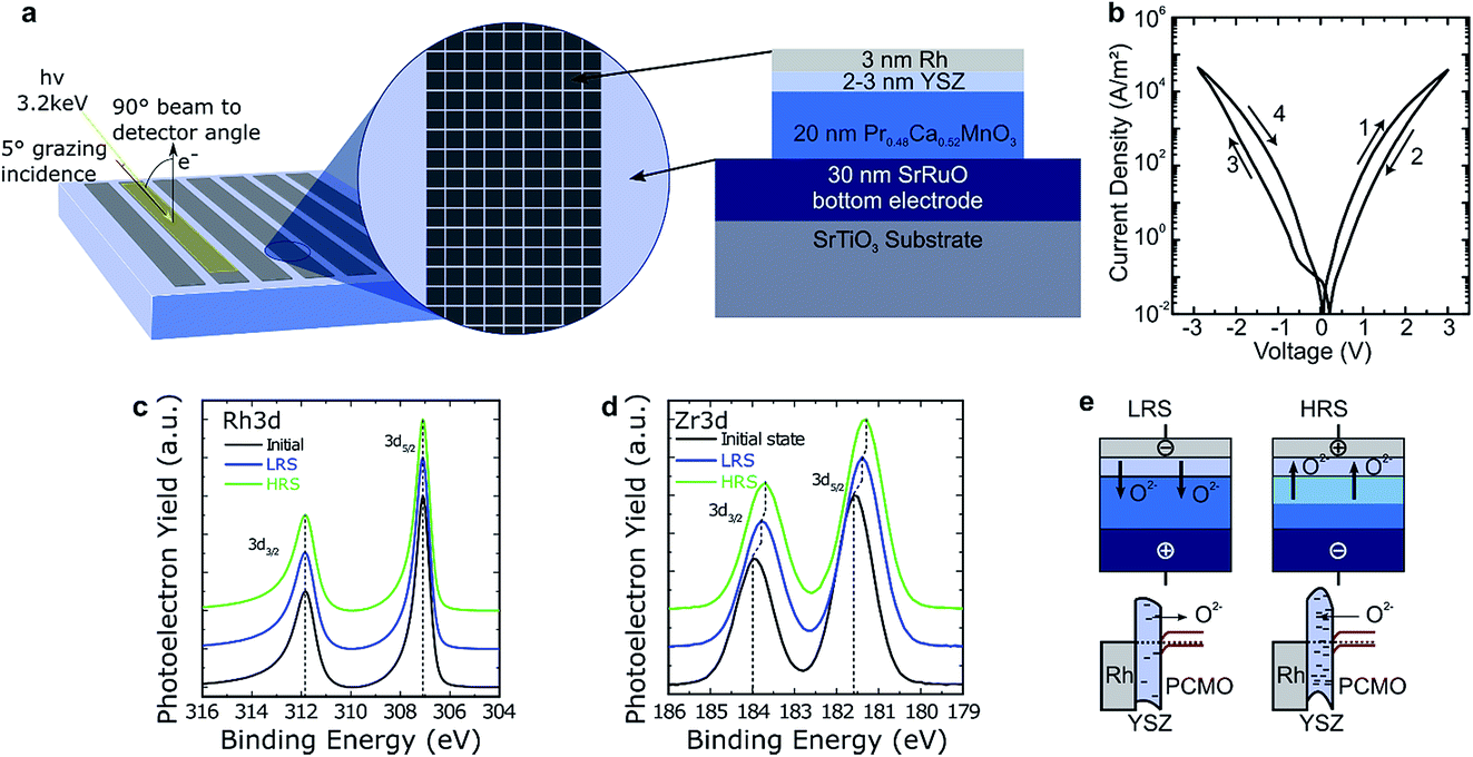 | ||
| Fig. 1 (a) Sketch of the sample layout of PCMO/YSZ devices with a side length of 50 μm and the geometry for HAXPES measurements with an illustration of the layer stack. The devices consist of Rh/YSZ/PCMO which is etched away outside the device area down to the SRO bottom electrode. (b) I–V curve of one PCMO/YSZ device. (c) and (d) show spectra for the core-levels of (c) Rh 3d and (d) Zr 3d for the initial, high and low resistive states, respectively. The photon energy was set to 3.2 keV. A Shirley background was subtracted from the data and they were normalized to the maximum intensity to allow for easier comparison of the line shapes and the peak positions. (e) Sketch of the movement of oxygen in the PCMO/YSZ stack with electrical biasing and corresponding change of the energy bands at the interface. | ||
2.2. HAXPES measurements
The HAXPES measurements were performed at the GALAXIES beamline of the French synchrotron radiation facility SOLEIL. A photon energy of 3200 eV was used as a compromise between maximizing the depth from which information could be obtained whilst minimizing the reduction in X-ray absorption cross-section that occurs with increasing photon energy. All the measurements were performed at room temperature, with an overall energy resolution of about 0.4 eV. More details are reported in the ESI of ref. 16.In order to take advantage of the high bulk sensitivity of HAXPES in grazing incidence geometry, which results in a beam footprint exceeding by far the single device area, we prepared special array-type samples (see also ref. 9). The arrays consisted of single devices 50 × 50 μm2 in size and arranged in arrays about 7 mm long and 0.5 mm wide, as shown in Fig. 1(a). The spacing between the devices was 10 μm. The large surface area of one array allows the adoption of a grazing incidence geometry with a grazing angle of 5° for the X-ray beam. This way, about 50 devices of the over one thousand devices present in one stripe of devices were probed simultaneously. The device resistance states were programmed ex situ, using a semi-automatic probe station, in advance. The devices were set to the LRS and HRS by voltage sweeps. One array was not programmed and was left in the initial or as-deposited state.
The core-level spectra for Rh 3d and Zr 3d are presented in Fig. 1(c) and (d). Both panels show the spectra for arrays in the initial state (as deposited) and after programming to the HRS and LRS. No changes of the line shape are evident in the core-level spectra of Rh and Zr, indicating the absence of changes in the chemical environment within the detection level of our measurements. The reproducibility of the Rh 3d line shapes indicate that the Rh remains metallic throughout switching and that no oxidation takes place.18 In contrast, clear shifts can be observed in the position of the Zr 3d core-level. In particular, both the LRS and the HRS are shifted to lower binding energies compared to the initial state, with the HRS shifted to about 0.1 eV lower binding energies than the LRS.
We interpret this result as the build-up of an electrostatic charge within the YSZ rather than a change in the Zr oxidation state, because the line shape does not change. We propose that the electrostatic charge originates from O2− ions (ionic space charge), which migrate into and out of the YSZ but are not charge-compensated by a valence change of the Zr ions.
Concerning the switching between the LRS and HRS, we conclude that oxygen ions move into the YSZ layer upon application of a positive bias to the top electrode, leading to an increase of the tunnel barrier height and hence to a decreased tunnel current in the HRS state, as sketched in Fig. 1(e). Conversely, applying a negative bias leads to the LRS state by removing oxygen ions from the YSZ. This modulation of the effective tunnel barrier height is caused by the excess negative charge that accumulates in the YSZ by the migration of oxygen ions. This description can be reproduced via I–V curve simulation of both resistance states based on asymmetric tunnel barriers with variable effective barrier heights.16 At the same time, it is consistent with our HAXPES observations, as negative charges increase the kinetic energy of the photoelectrons, shifting the spectrum towards lower binding energies. In the same sense, by removing negative charge from the interface, the spectrum shifts towards higher binding energies. This model is in general similar to the mechanism suggested for PCMO/tunnel oxide devices in ref. 19, however it slightly differs since we observed only a less negatively charged YSZ barrier in the LRS and not a positively charged region as suggested by the authors.
3. TaOx/HfO2 layer stacks
3.1. Resistive switching properties
The second resistively switching layer stacks chosen for our studies were Rh/HfO2/TaOx/Ta and Pt/HfO2/TaOx/Ta heterostructures. The heterostructures were prepared by DC sputtering on a silicon substrate covered with 430 nm thermal silicon oxide. A 50 nm thick tantalum film was deposited from a metallic target with a power of 30 W in pure argon under high pressures (7 × 10⁻³ mbar). Afterwards, a 5 nm TaOx thick film was sputter-deposited in situ at 3 × 10⁻² mbar by reactive DC sputtering in a 97% Ar and 3% O2 atmosphere with a power of 35 W. Based on our previous XPS studies, these deposition parameters result in a considerable amount of metallic Ta in the thin films, giving rise to electron conducting TaOx thin films. The HfO2 tunnel barrier was subsequently deposited by DC sputtering from a metallic Hf target in 67% Ar and 33% O2 atmosphere at 3 × 10⁻² mbar with a power of 15 W. Because of the increased oxygen partial pressure, the HfO2 thin films are stoichiometric and highly insulating. The evaporated Rh (Pt) top electrodes have a thickness of 2 nm (25 nm). Samples for electrical testing were prepared by patterning of the Pt top electrode to squares of 10 × 10 μm2, 20 × 20 μm2 and 30 × 30 μm2. Fig. 2(a) shows I–V curves for device stacks with three different areas. As can be seen in Fig. 2(b), the current scales well with the device area, confirming an interface-type switching mechanism. Both SET and RESET show a gradual-type of switching, as was the case for the PCMO/YSZ stacks. In order to check the suitability of the devices for in operando measurements, we performed repeated cycling of our devices. As can be seen in Fig. 2(c), stable switching has been observed for more than 40 cycles, which is sufficient to perform in operando measurements.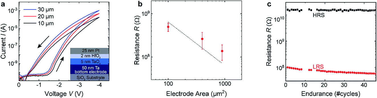 | ||
| Fig. 2 (a) I–V curves of HfO2/TaOx square test devices with different side lengths. (b) Dependence of the LRS resistance on the device area read-out with −1 V for the samples shown in (a). (c) Endurance measurements of a 30 × 30 μm2 devices read-out with −1 V at room temperature. | ||
The samples fabricated for in operando measurements possess an edge length of 60 × 200 μm2 and the same sample geometry as the YSZ/PCMO samples, as sketched in Fig. 4(a). The surroundings of the devices are covered by SiO2 to guarantee electrical insulation and prevent any photoemission contribution from the bottom electrode. The I–V curves of the devices looked similar to the small test devices shown in Fig. 2(a), besides that the current increased as expected from the area scaling behaviour.
3.2. In operando HAXPES measurements
In order to perform in situ biasing during HAXPES measurements, the devices were grounded through the continuous bottom electrode layer, while the top Rh electrode was electrically connected externally to a Keithley source measure unit. Before the sample carrier was introduced into the vacuum chamber at the GALAXIES beamline, several voltage cycles were applied to the connected device to test the electrical connections.We started HAXPES measurement on our device while applying a sequence of negative voltages 0 V → −1 V → −2 V → −0.2 V → 0 V to our devices and recorded the resistance of the devices as depicted in Fig. 3(a). We observed a sudden drop in the resistance at 120 s while applying constant voltage. After increasing the voltage to −2 V, the resistance decreased further in several sudden jumps until reaching a resistance of ∼2000 Ω after 400 s. Due to the current limit of 100 μA, the cell voltage dropped to −0.2 V simultaneously. Fig. 3(b) shows the I–V curve that was recorded subsequently. The I–V curve has a completely different shape than the I–V curves recorded from the device before (similar curves are shown in Fig. 2(a)) and looks very similar to filamentary switching HfO2 devices.20,21 In particular, the I–V curve in Fig. 3(b) exhibits a sharp SET process in the negative branch and a resistance ratio between the HRS and LRS of about three orders of magnitude, which is about two orders of magnitude higher than in the interface-type switching mode of the cell observed before. We can therefore conclude that a filament was formed within the HfO2 layer during DC electrical biasing in the vacuum chamber. The exposure of the sample to the synchrotron beam might have induced oxygen vacancies in the HfO2 layer similarly as reported for SrTiO3 single crystals,22 and might thereby have promoted this forming process.23
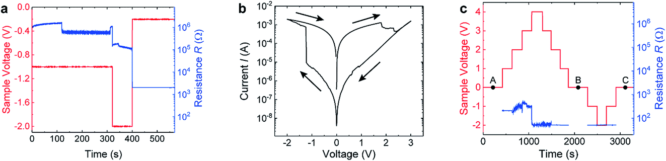 | ||
| Fig. 3 Details of the electrical biasing procedure during in operando measurements. (a) First biasing scheme which resulted in a transformation to filamentary switching. Timing of the voltage steps (red) and the corresponding device resistance (blue). (b) I–V curve recorded after applying the voltage sequence shown in (a). (c) Biasing scheme employed for the in operando HAXPES measurements shown in Fig. 4. Timing of the voltage steps (red) and resulting resistance (blue). The different devices states, namely (A), (B), and (C) at which the core-level spectra at 0 V were recorded are marked with black points. | ||
Fig. 4(b) and (c) show the HAXPES spectra collected with an X-ray photon energy of 3.2 keV with an incidence angle of 45°, illuminating the device area of the selected device. The photoelectrons were detected at 45° emission geometry. The overall spectral resolution was determined to be 0.40 eV. With these settings, we were able to detect a significant signal intensity for the core level peaks Rh 3d (top electrode), Hf 4f (tunnel barrier), Ta 4f (conductive oxide layer), and O 1s (HfO2, Ta2O5 and surrounding SiO2). In order to determine the peak position and the spectral intensity of each term, all the core level spectra were analysed with CasaXPS Version 2.3.17. A Shirley background profile was subtracted from all of them. The peaks of the oxides (Ta 4f, Hf 4f) were fitted using Voigt functions while the core level spectra of the metal (Rh 3d) were fitted using a Doniach–Sunjic lineshape. The spectra clearly indicate that we were able to probe both the Rh/HfO2 as well as the HfO2/TaOx/Ta interfaces with a good signal to noise ratio. The first Ta 4f and Hf 4f spectra recorded at 0 V (corresponding to state (A) in Fig. 3(c)) are displayed in Fig. 4(b). The spectra can be nicely reproduced by a fit with Ta5+, Ta4+, Ta0 and Hf4+ components. The main contribution to the Ta 4f spectrum can be assigned to Ta5+, however, a significant amount of Ta4+ and metallic Ta0 is present as well. It is important to note that there is no evidence of a suboxide component in the HfO2 layer.
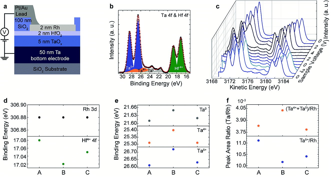 | ||
| Fig. 4 (a) Sketch of the layout for the in operando measurement of the TaOx/HfO2 layer stacks. (b) Ta 4f and Hf 4f core-level spectra recorded at 0 V in state (A) of Fig. 3(b) together with the fit of the data. (c) Ta 4f and Hf 4f core-level spectra recorded at different sample voltages. (d) Binding energy of the Rh 3d and Hf 4f peak for the different states (A)–(C) of the device. (e) Binding energy of the different Ta 4f spectral components in the different states (A)–(C) of the device. (f) Ta/Rh peak area ratio of Ta5+ and (Ta4+ + Ta0) species in the different states (A)–(C) of the device. | ||
The core-level position of the Rh spectra (not shown) shifts linearly with the voltage as observed for the PCMO/YSZ devices. Fig. 4(c) shows the voltage dependence of the Ta 4f and Hf 4f core level spectra recorded during in situ biasing with voltages in a range of 4 V to −2 V according to the biasing scheme shown in Fig. 3(c). The spectra shifted linearly to higher (lower) kinetic energy for negative (positive) applied voltage, proving that the devices are electrically biased in a proper way. The shift of the core-level spectra is different from the magnitude of the applied voltage. This is due to a significant portion of voltage drop at the series resistance of the measurement equipment and the electrical connections. However, the actual voltage drop across the device is provided directly by the relative shift of the core-level spectra for the Rh and Ta layers.
For a closer inspection, we determined the peak positions of the spectra collected at 0 V, i.e., after initial negative bias (state (A)), after positive biasing (state (B)) and after negative biasing (state (C)). The determined shifts of the Rh 3d and Hf 4f core-level peaks and, for the Ta 4f, core-level peaks of the different Ta valence state contributions in the three different states ((A)–(C)) are shown in Fig. 4(d) and (e), respectively. The Rh 3d peak position is constant in the three states, indicating that no changes are taking place in the Rh during electrical biasing. In contrast, the Hf 4f binding energy decreases slightly from state (A) to state (B) and increases again in state (C). All three Ta binding energy positions show the opposite trend, namely they increase from state (A) to state (B) and decrease again in state (C). Assuming a shift of the relative position of the Fermi-level within the band gap of the TaOx layer as the origin of this shift, this indicates a reduction from state (A) to state (B) and an oxidation of the layer from state (B) to state (C). This is fully consistent with the changes in the spectral weight of the different Ta valences shown in Fig. 4(f). In particular, the Ta5+ contribution is higher at state (A) and (C) and the lower valence state contributions increase in state (B).
Since we did not see a change in the spectral weight of HfO2 in the different states, we attribute the observed shift of the kinetic energies to a negative charging of the HfO2 layer from state (A) to state (B) and a positive charging from state (B) to state (A). Keeping in mind that positive voltage steps were applied from state (A) to state (B) and negative voltage steps between state (B) and state (C) (see Fig. 3(c)), the observed effect would be consistent with a shift of negatively charged oxygen ions between the TaOx and the HfO2 layer. The suggested mechanism is sketched in Fig. 5. By applying a negative voltage to the top electrode, oxygen moves from the HfO2 layer into the TaOx layer, leading to a less negatively charged HfO2−δ tunnel barrier and a more oxidized TaOx layer (Fig. 5(a)). In turn, by applying a positive voltage to the top electrode, the oxygen moves from the TaOx layer into the HfO2−δ layer, leading to a more negatively charged HfO2 tunnel barrier and a more reduced TaOx−δ layer (Fig. 5(b)). Thus, the HfO2−δ tunnel barrier decreases (increases) due to positive (negative) charging induced by the motion of the oxygen ions (cf.Fig. 5).
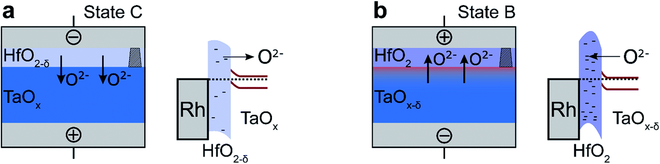 | ||
| Fig. 5 Sketch of the interface-type switching of the TaOx devices with a parallel conducting filament current path for negative (a) and positive (b) bias polarities. The filament is indicated by the shaded regions in the right part of the tunnel barrier. The change of the energy bands at the interface resulting from the movement of oxygen in the TaOx/HfO2 stack is shown on the right of the stacks. | ||
This process is the same as that proposed for the interface switching PCMO/YSZ devices. However, one should keep in mind that the electrical behaviour of the TaOx/HfO2 devices is completely different. The devices have been transformed to a filamentary switching mode during the first DC biasing step as shown in Fig. 2(b). In order to assign the systematic change of the observed spectral fingerprint to the resistance changes of the device, we will now consider in detail the resistance changes observed in the three different states. In state (A), the device is in an LRS and is expected to switch into an HRS in state (B) after the application of a positive bias sequence. However, as can be seen in Fig. 3(c), the device resistance further decreased in state (B). Afterwards, we applied a negative voltage, which would nominally switch the device back to the LRS. However, it can be seen in Fig. 3(c) that the resistance remains unchanged during the last biasing step. Therefore, we can conclude that we have induced a permanent breakdown of the device in the filament region (sketched as the shaded region in Fig. 5), which determines the device resistance. Therefore, the observed systematic changes of the core-level shifts and the spectral distribution between the different Ta valence states are not correlated with the resistance state of the device. Assuming a typical filament size in the nm regime, the relative change of the electronic structure would be insufficient in order to be detected within the device area of 60 × 200 μm2 (even a very large filament of 1 μm diameter would contribute only ∼0.01% of the total HAXPES intensity). Therefore, we are unable to draw any conclusions about the chemical composition of the filament and we have to assume that the observed chemical changes take place at the interface region of the entire device area. These observations imply that the reversible ionic motion at the whole interface region (which presumably gives rise to the interface-type resistive switching in both PCMO/YSZ and TaOx/HfO2 devices) is sustained despite the filament formation and the final breakdown process. This has important implications for the HAXPES analysis of filamentary resistive switching devices, since the parallel processes might lead to misinterpretations of the observed chemical changes if they are attributed to the nanoscale filament region within 100 μm-sized device areas.
3.3. Finite element simulations
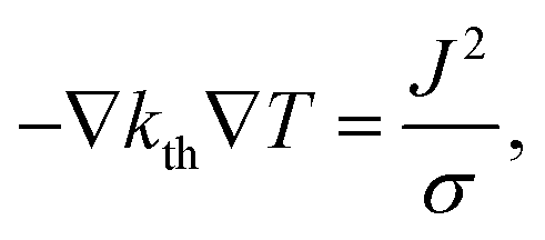
In order to assess the scenario of having parallel paths of ionic motion within and outside the filament region, we consider the impact of the different driving forces for ionic motion in our devices. Generally, in contrast to interface-type switching, which is mainly field-driven, filamentary switching involves local Joule heating.24 The concurrent temperature increase within the filament leads to an acceleration of the ion migration. Moreover, the local temperature increase leads to a positive feedback loop (a so-called thermal runaway) during the SET transition and eventually a very sharp current increase.25 Such an abrupt current jump is also evident in Fig. 3(b) at about −1.25 V. For interface-type switching, the local current density is typically too low to result in a significant temperature increase. Thus, a thermal runaway process cannot occur and SET and RESET transitions appear more gradual (see Fig. 2).To evaluate the temperature distribution in the TaOx/HfO2 layer stack, an electro-thermal simulation model was used. To reduce the numerical complexity, we considered the two-dimensional axisymmetric structure shown in Fig. 6(a). It consists of a 430 nm-thick SiO2 bottom layer, a 50 nm-thick Ta electrode, a 5 nm-thick TaOx layer, a 2 nm-thick HfO2 layer, and a 2 nm-thick Rh electrode. The HfO2 layer is divided into a filamentary HfO2−γ region with radius rfil at the symmetry axis and a less conducting HfO2 matrix region. An insulating 100 nm-thick SiO2 layer is located on top of the Rh at the outer rim of the stack covering 11 μm of the Rh electrode. A 130 nm-thick Au/Pt electrode covers 9 μm of the Rh electrode and the SiO2 spacer.
To calculate the temperature distribution in this structure, the static heat transfer equation
 | (1) |
| −∇J = ∇σ∇φ = 0 | (2) |
| σmatrix = J(Vapp)dHfO2/Vapp. | (3) |
The conductivity of the filament σfil is calculated by assuming that the total current during filamentary switching flows through the filament. The total cell resistance Rcell can then be approximated by the resistance of the filament Rfil and the spreading resistance Rspread in the TaOx film according to
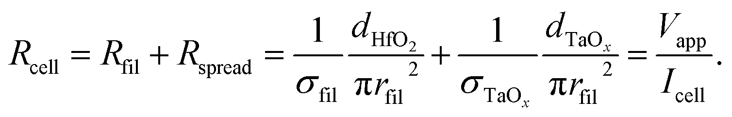 | (4) |
Solving the equation for σfil yields
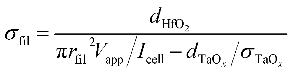 | (5) |
This system of equations is completed by an appropriate set of boundary conditions for solving the partial differential eqn (1) and (2), which are shown in Fig. 6(a). The voltage Vapp is applied to the top electrode, while the bottom electrode is set to ground. For all other boundaries a Neumann boundary condition is used setting the normal charge flow to zero. The temperature at the bottom of the SiO2 layer is set to T = 300 K, as it is in contact with the measurement stage. For all other boundaries the heat flux is set to zero.
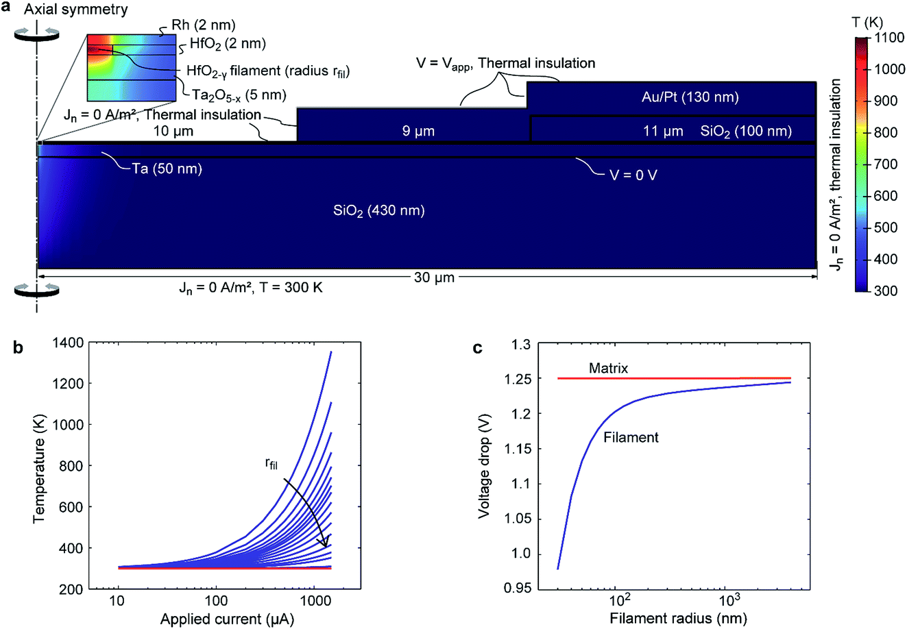 | ||
| Fig. 6 (a) Simulation geometry with boundary conditions. Note that the geometry is scaled with a factor of 10 in the vertical direction for better visibility. The colour map shows the temperature distribution at −1.5 mA for a filament radius of 50 nm. The zoom-in shows the temperature distribution in the filament. (b) Average temperature in the filament (blue solid lines) and the surrounding matrix (red solid line) as a function of the cell current for different filament radii, i.e. 30 nm, 40 nm, 50 nm, 60 nm, 70 nm, 80 nm, 90 nm, 100 nm, 120 nm, 150 nm, 200 nm, 300 nm, 500 nm, 800 nm, 1 μm, 4 μm. The average temperature in the surrounding matrix is about the same (1 K deviation) for all radii. (c) Average voltage drop over the filament region (blue solid line) and the matrix region (red solid line) as a function of the filament radius for a cell current of −1.5 mA. | ||
As the exact filament radius is not known, the electro-thermal simulations are performed for different filament radii. To simulate the temperature distribution during the filamentary SET transition, the applied voltage is set to Vapp = −1.25 V and the current Icell is varied from −10 μA to −1.5 mA. The latter leads to a change of the filament conductivity according to eqn (5).
Fig. 6(a) shows the simulated temperature distribution at Icell = −1.5 mA and rfil = 50 nm. The highest temperature evolves in the filament itself, while the matrix remains at a low temperature. This observation is valid for all simulations performed as shown in Fig. 6(b). The temperature within the filament is a strong function of the current as well as the filament radius. Based on the assumption that the abrupt current increase during the filamentary SET transition is due to a thermal runaway process, a minimum temperature increase of 5 K should occur at the lower current level of the current jump.25 This is only true for filament radii smaller than 50 nm. Another interesting result is the average voltage drops over the filament and the surrounding HfO2 matrix. The voltage drop over the filament increases with increasing filament radius. The reason is the increased spreading resistance of the TaOx layer below the filament for small filament radii. In contrast, the voltage drop over the HfO2 matrix is constant and equals the applied voltage despite the presence of the highly conducting filament.
In a second simulation study, the temperature during interface-type switching was estimated. For this purpose, we considered only a homogenous HfO2 layer without a filament, which corresponds to the situation in our device before the forming step in Fig. 3(a). According to Fig. 2 the highest electrical power is dissipated at the turning point of the SET transition, i.e. Vapp = −4 V and J = −2 × 10⁶ A m−2. Using this data pair, the conductivity of the HfO2 layer is recalculated using eqn (3). The simulation result shows a slight temperature increase of the whole sample of about 10 K. The voltage drop over the HfO2 layer again equals the applied voltage.
4. Discussion
Based on the experimental observations and the simulation results, we can draw several conclusions about the switching processes in bilayers of one conductive oxide layer and one insulating tunnel oxide. Without formation of a filament, application of positive biases induces oxygen ion migration from the conductive oxide into the tunnel oxide across the entire device area, thus charging the barrier and resulting in an HRS. This process appears to be responsible for the interface-type switching in both PCMO/YSZ and TaOx/HfO2 devices in the as-prepared state. For the TaOx/HfO2 devices, a second, filamentary switching mode can be stabilized after the forming process occurring during DC biasing in vacuum under synchrotron irradiation.Our simulations show that this type of switching goes along with local Joule-heating, leading to very high filament temperatures, especially for small filament radii (note that for the thermal runaway leading to filamentary resistive switching, filament radii below 50 nm are required). At the same time, our simulations reveal that the temperature in the tunnel oxide matrix remains close to RT for the interface-type switching, and even if filamentary switching with high local temperatures occurs in parallel. In both cases, the voltage drop over the tunnel oxide layer is constant and equals the applied voltage. As the HAXPES signal used to derive the switching mechanism originates from the entire device area, this means that the oxygen ion motion for the whole interface area occurs close to RT.
To examine whether such purely field-driven ionic motion may lead to the observed changes in the electronic structure and the corresponding resistance change, we consider the Mott–Gurney equation, which can be used as a first approximation to calculate the field-induced velocity of oxygen ions:29
 | (6) |
5. Conclusions
We have investigated in detail non-filamentary, resistively switching PCMO/YSZ and TaOx/HfO2 heterostructures by HAXPES analysis. For the PCMO/YSZ devices, our data provide conclusive experimental evidence that the resistance change of the devices is determined by electrostatic charging of the YSZ tunnel barrier, caused by the exchange of oxygen ions between the YSZ and the PCMO layer. The chemical changes observed in the TaOx/HfO2 stack during electrical biasing are also consistent with a shift of oxygen vacancies from the TaOx layer to the HfO2 layer and a negative charging of the HfO2 tunnel oxide for positive biasing during the SET process. However, due to an estimated filament size on the order of a few μm or less, the relative change of the electronic structure is insufficient in order to be detected on device areas of 60 × 200 μm2 used for the HAXPES measurements. We therefore attribute the observed changes of the metal core-level spectra to the changes of the electronic structure across the whole device area taking place as a side effect during electrical biasing. Since the conductivity will be dominated by the highly conductive filament, the observed changes of the electronic structure on the whole device area have a negligible influence on the device resistance. However, it is important to note that we could thereby evidence a co-existence of strongly temperature-accelerated ionic motion within the filament, with ionic motion taking place over the whole device area. Finite element simulations of the field and temperature distribution during device operation show that there is insufficient Joule heating to promote ionic motion outside the filament region. Instead, the large field drop at the tunnel barrier induces the detected ionic motion near room temperature. This ionic motion outside the filament region might explain the formation of new filament sites during repeated switching31 and might therefore have important implications for device reliability issues such as variability and endurance.Author contributions
F. B., B. A., K. S., R. D. and C. B. conceived and designed the experiments. B. A. and K. S. fabricated the samples and performed electrical testing. F. B., F. O., F. M., C. B. and T. H. performed the in operando HAXPES analysis. K. S., C. B. and T. H. analysed the data. S. M. performed the finite element simulations. R. D., C. B., T. H. and S. M. wrote the manuscript. G. P., R. W. and R. D. supervised the research. All authors discussed the results and commented on the manuscript.Conflicts of interest
There are no conflicts to declare.Acknowledgements
The HAXPES analysis was performed at the GALAXIES beamline at SOLEIL under the proposal 20140991 and 20160918. The authors thank the beamline staff Jean-Pascal Rueff and Denis Ceolin for their support. Funding from the DFG (German Science Foundation) within the collaborative research center SFB 917 “Nanoswitches” is gratefully acknowledged. RD and CB also acknowledge funding from the W2/W3 program of the Helmholtz association.References
- D. Ielmini and R. Waser, Resistive Switching: From Fundamentals of Nanoionic Redox Processes to Memristive Device Applications, Wiley-VCH, 2016 Search PubMed.
- R. Waser, R. Dittmann, G. Staikov and K. Szot, Adv. Mater., 2009, 21, 2632 CrossRef CAS.
- A. Sawa and R. Meyer, Interface-Type Switching, in Resistive Switching, ed. D. Ielmini and R. Waser, Wiley-VCH, Weinheim, 2016 Search PubMed.
- A. Sawa, Mater. Today, 2008, 11, 28 CrossRef CAS.
- C. Baeumer, N. Raab, T. Menke, C. Schmitz, R. Rosezin, P. M. Müller, M. Andrä, V. Feyer, R. Bruchhaus, F. Gunkel, C. M. Schneider, R. Waser and R. Dittmann, Nanoscale, 2016, 8, 13967 RSC.
- M. Sowinska, T. Bertaud, D. Walczyk, S. Thiess, P. Calka, L. Alff, C. Walczyk and T. Schroeder, J. Appl. Phys., 2014, 115, 204509 CrossRef.
- L. A. Walsh, G. Hughes, P. K. Hurley, J. Lin and J. C. Woicik, Appl. Phys. Lett., 2012, 101, 241602 CrossRef.
- M. Sacchi, F. Offi, P. Torelli, A. Fondacaro, C. Spezzani, M. Cautero, G. Cautero, S. Huotari, M. Grioni, R. Delaunay, M. Fabrizioli, G. Vanko, G. Monaco, G. Paolicelli, G. Stefani and G. Panaccione, Phys. Rev. B: Condens. Matter Mater. Phys., 2005, 71, 155117 CrossRef.
- A. Herpers, C. Lenser, C. Park, F. Offi, F. Borgatti, G. Panaccione, S. Menzel, R. Waser and R. Dittmann, Adv. Mater., 2014, 26, 2730 CrossRef CAS PubMed.
- F. Borgatti, C. Park, A. Herpers, F. Offi, R. Egoavil, Y. Yamashita, A. Yang, M. Kobata, K. Kobayashi, J. Verbeeck, G. Panaccione and R. Dittmann, Nanoscale, 2013, 5, 3954 RSC.
- J. Fujii, M. Sperl, S. Ueda, K. Kobayashi, Y. Yamashita, M. Kobata, P. Torelli, F. Borgatti, M. Utz, C. S. Fadley, A. X. Gray, G. Monaco, C. H. Back, G. van der Laan and G. Panaccione, Phys. Rev. Lett., 2011, 107, 187203 CrossRef CAS PubMed.
- T. Pincelli, V. Lollobrigida, F. Borgatti, A. Regoutz, B. Gobaut, C. Schlueter, T. Lee, D. J. Payne, M. Oura, K. Tamasaku, A. Y. Petrov, P. Graziosi, F. M. Granozio, M. Cavallini, G. Vinai, R. Ciprian, C. H. Back, G. Rossi, M. Taguchi, H. Daimon, G. van der Laan and G. Panaccione, Nat. Commun., 2017, 8, 16051 CrossRef CAS PubMed.
- E. Slooten, Z. Zhong, H. J. A. Molegraaf, P. D. Eerkes, S. de Jong, F. Massee, E. van Heumen, M. K. Kruize, S. Wenderich, J. E. Kleibeuker, M. Gorgoi, H. Hilgenkamp, A. Brinkman, M. Huijben, G. Rijnders, D. H. A. Blank, G. Koster, P. J. Kelly and M. S. Golden, Phys. Rev. B: Condens. Matter Mater. Phys., 2013, 87, 85128 CrossRef.
- F. Borgatti, I. Bergenti, F. Bona, V. Dediu, A. Fondacaro, S. Huotari, G. Monaco, D. A. MacLaren, J. N. Chapman and G. Panaccione, Appl. Phys. Lett., 2010, 96, 43306 CrossRef.
- T. Bertaud, M. Sowinska, D. Walczyk, C. Walczyk, S. Kubotsch, C. Wenger and T. Schroeder, E-Mrs 2012 Spring Meeting, Symposium M: More Than Moore: Novel Materials Approaches For Functionalized Silicon Based Microelectronics, 2012, vol. 41, p. 12018 Search PubMed.
- B. Arndt, F. Borgatti, F. Offi, M. Phillips, P. Parreira, T. Meiners, S. Menzel, K. Skaja, G. Panaccione, D. A. MacLaren, R. Waser and R. Dittmann, Adv. Funct. Mater., 2017, 1702282 CrossRef.
- E. Kroeger, A. Petraru, A. Quer, R. Soni, M. Kallaene, N. A. Pertsev, H. Kohlstedt and K. Rossnagel, Phys. Rev. B, 2016, 93, 235415 CrossRef.
- L. Marot, D. Mathys, G. De Temmerman and P. Oelhafen, Surf. Sci., 2008, 602, 3375 CrossRef CAS.
- R. Meyer, L. Schloss, J. Brewer, R. Lambertson, W. Kinney, J. Sanchez and D. Rinerson, 2008 9th Annual Non-Volatile Memory Technology Symposium, Proceedings, 2008, p. 54 Search PubMed.
- Y. H. Wu, D. J. Wouters, P. Hendrickx, L. Zhang, Y. Y. Chen, L. Goux, A. Fantini, G. Groeseneken and M. Jurczak, IEEE Electron Device Lett., 2013, 34, 414 CAS.
- A. Hardtdegen, C. La Torre, H. Zhang, C. Funck, S. Menzel, R. Waser and S. Hoffmann-Eifert, 2016 IEEE 8th International Memory Workshop (IMW), Paris, France, May 15–18, 2016, p. 1 Search PubMed.
- L. Dudy, M. Sing, P. Scheiderer, J. D. Denlinger, P. Schütz, J. Gabel, M. Buchwald, C. Schlueter, T.-L. Lee and R. Claessen, Adv. Mater., 2016, 28, 7443 CrossRef CAS PubMed.
- S. U. Sharath, M. J. Joseph, S. Vogel, E. Hildebrandt, P. Komissinskiy, J. Kurian, T. Schroeder and L. Alff, Appl. Phys. Lett., 2016, 109, 173503 CrossRef.
- S. Menzel, M. Waters, A. Marchewka, U. Böttger, R. Dittmann and R. Waser, Adv. Funct. Mater., 2011, 21, 4487 CrossRef CAS.
- K. Fleck, C. La Torre, N. Aslam, S. Hoffmann-Eifert, U. Böttger and S. Menzel, Phys. Rev. Appl., 2016, 6, 064015 CrossRef.
- C. D. Landon, R. H. T. Wilke, M. T. Brumbach, G. L. Brennecka, M. Blea-Kirby, J. F. Ihlefeld, M. J. Marinella and T. E. Beechem, Appl. Phys. Lett., 2015, 107, 023108 CrossRef.
- M. A. Panzer, M. Shandalov, J. A. Rowlette, Y. Oshima, Y. W. Chen, P. C. McIntyre and K. E. Goodson, IEEE Electron Device Lett., 2009, 30, 1269 CAS.
- C. M. M. Rosario, B. Thoener, A. Schoenhals, S. Menzel, M. Wuttig, R. Waser, N. A. Sobolev and D. J. Wouters, Appl. Phys. Lett., 2018, 112, 213504 CrossRef.
- S. Starschich, S. Menzel and U. Böttger, Appl. Phys. Lett., 2016, 108, 032903 CrossRef.
- A. R. Genreith-Schriever and R. A. De Souza, Phys. Rev. B, 2016, 94, 224304 CrossRef.
- C. Baeumer, R. Valenta, C. Schmitz, A. Locatelli, T. O. Mentes, S. P. Rogers, A. Sala, N. Raab, S. Nemsak, M. Shim, C. M. Schneider, S. Menzel, R. Waser and R. Dittmann, ACS Nano, 2017, 11, 6921 CrossRef CAS PubMed.
| This journal is © The Royal Society of Chemistry 2019 |