
Visualization of label-free titanium dioxide nanoparticle deposition on surfaces with nanoscale roughness†
Negin
Kananizadeh
 ab,
Darin
Peev
bc,
Thompson
Delon
ab,
Eva
Schubert
bc,
Shannon
Bartelt-Hunt
ab,
Mathias
Schubert
*bcde,
Jianming
Zhang
f,
Petra
Uhlmann
e,
Albena
Lederer
e and
Yusong
Li
*ab
ab,
Darin
Peev
bc,
Thompson
Delon
ab,
Eva
Schubert
bc,
Shannon
Bartelt-Hunt
ab,
Mathias
Schubert
*bcde,
Jianming
Zhang
f,
Petra
Uhlmann
e,
Albena
Lederer
e and
Yusong
Li
*ab
aDepartment of Civil Engineering, University of Nebraska-Lincoln, Lincoln, NE 68588, USA. E-mail: yli7@unl.edu
bCenter for Nanohybrid Functional Materials, University of Nebraska-Lincoln, Lincoln, NE 68588, USA
cDepartment of Electrical and Computer Engineering, University of Nebraska-Lincoln, Lincoln, NE 68588, USA. E-mail: schubert@engr.unl.edu
dDepartment of Physics, Chemistry, and Biology (IFM), Linkoping University, Linkoping, 58183, Sweden
eLeibniz Institute of Polymer Research (IPF) Dresden, Dresden, D 01005, Germany. E-mail: uhlmannp@ipfdd.de; lederer@ipfdd.de
fState Key Laboratory of Hydraulics and Mountain River Engineering, Sichuan University, Chengdu, 610065, China
First published on 29th November 2018
Abstract
Understanding the transport of engineered nanoparticles (ENPs) and their interaction with environmental surfaces is critical to predicting their fate and environmental implications. Here, we report an innovative technique to visualize and quantify the deposition of titanium dioxide nanoparticles (TiO2NP) on engineered surfaces with nanoscale roughness, i.e., slanted columnar thin films (SCTFs). The attachment of TiO2NP on the surface of SCTFs changed the optical property of SCTFs, which was detected using a generalized ellipsometry (GE)-based instrument, an anisotropy contrast optical microscope (ACOM). An anisotropic effective medium model was applied to quantitatively analyze ACOM images of SCTF surfaces, which provided the mass distribution of TiO2NP. The TiO2NP mass measured by ACOM was in good agreement with the known amount of TiO2NP mass dispersed by controlled piezoelectric plotting. The detection of a few picograms of nanoparticle mass by an individual pixel measuring 7 × 7-micrometer squared was demonstrated. Further, a glass microfluidic channel with SCTF embedded was developed. The areal mass density of attached TiO2NP on SCTF surfaces as they flow through the channel under various flow rates was quantitatively measured in situ. At the end of the experiment, the distribution of the attached TiO2NP on the SCTF surface was visualized. The averaged mass density estimated by integrating the distribution map was in close agreement with the estimation from dynamic measurements and between repeating experiments. The capability of this novel technique to sense, quantify and visualize the mass distribution of TiO2NP provides a valuable approach to investigate the behavior of nanoparticles at the interface of flow and rough surfaces.
Environmental significanceUnderstanding the transport of engineered nanoparticles (ENPs) and their interaction with environmental surfaces is critical to predicting their fate and environmental implications. Titanium dioxide nanoparticles (TiO2NPs) are one of the most widely used ENPs in the commercial industry, which were detected in the environment. Based on the principles of generalized ellipsometry (GE), we demonstrated an innovative, label-free method to visualize and quantify the deposition and transport of TiO2NPs on engineered surfaces with nanoscale roughness, i.e., slanted columnar thin film (SCTF) surfaces. |
1. Introduction
Engineered nanoparticles (ENPs) are widely used in many commercial products, which can lead to their release into the environment during use or after disposal. The production of titanium dioxide nanoparticles (TiO2NPs), one of the most widely used ENPs in commercial industry, was estimated to be 2.4 million tons in the US by 2025, and 3 to 30 percent of that may end up in water bodies.1,2 Recent work has found that the toxicity of TiO2NP can be increased by over an order of magnitude when they are exposed to ultraviolet light, a typical case in clear water.3 Understanding the transport of ENPs and their interaction with environmental surfaces is critical to predicting their fate and environmental implications.The majority of ENP transport studies have been conducted using a cylindrical column packed with environmental media, i.e., silica sands, glass beads, or soils.3–10 By measuring the concentration change of ENPs at the inlet and outlet of the column, deposition of ENP in the environmental media can be estimated using a classical filtration theory or a modified version of the theory. Although column experiments present a relatively realistic setup to environmental porous media, the interaction between ENPs and surfaces cannot be directly measured. In addition to traditional column experiments, the deposition of ENPs onto solid surfaces has been recently measured using quartz crystal microbalance with dissipation (QCM-D).11–13 Although QCM-D can measure the direct interaction between ENPs and a surface, most studies used very flat silica or metal oxide surfaces to mimic natural soil and sediment surfaces, which could be an oversimplification by totally neglecting the influence of surface roughness. Recently, a model rough surface12 was incorporated onto QCM-D surfaces to investigate the impact of surface roughness on TiO2NP deposition. This approach provides a method to directly measure the interaction of TiO2NP and a model rough surface; however, QCM-D lacks visualization of the attached ENPs on the surfaces.
To better evaluate and visualize ENPs deposition, microfluidic channels, in conjunction with various visualization techniques, were developed.14–19 For example, an innovative micromodel system with well-arranged 2-D cylindrical collectors was used to visualize ENP deposition and quantify the single collector efficiency factor.19 Such systems, however, rely on the fluorescent labeling of ENPs for visualization. The use of fluorescent labels may modify the properties of a given ENP, for example TiO2NP, or may interfere with the interaction between TiO2NPs and surfaces. Therefore, it is often desirable to obtain optical images without applying fluorescent labels. Previously, Guzman et al. used a 2-D micromodel of porous media to investigate the effect of pH on TiO2NPs aggregation and transport in porous media.14 The concentration of TiO2NP at the effluent of the 2-D micromodel was measured using UV-vis, and a CCD camera was used to visualize the pore clogging. Here, the distribution of particle aggregates was only visualized qualitatively.
In this work, we present the application of an innovative label-free imaging technique sensitive to nanoscopic objects – Anisotropy Contrast Optical Microscopy (ACOM)20 – to obtain images and quantify the mass distribution of TiO2NP attached to engineered porous, optically anisotropic, slanted columnar thin films (SCTFs). ACOM uses principles of generalized ellipsometry (GE), a highly accurate, non-destructive, and non-invasive optical method,21,22 which measures the change in polarization when light reflects off or transmits through a sample.20,23–28 Here, SCTFs served as an anisotropic substrate for GE measurements, as well as a surface with a controlled roughness height. For the first step of our investigation, the change in the anisotropic optical response of SCTFs due to local deposition of TiO2NP drops with known mass on the surface of SCTF was imaged and measured using ACOM statically in the air ambient. We then used this technique to measure and visualize the deposition of TiO2NP onto SCTF surfaces inside a microfluidic channel dynamically under flow conditions. Here, an innovative approach to embed SCTF in a glass microfluidic channel was developed, which is not invasive to the SCTF thin films.
2. Materials and methods
2.1. Nanoparticle preparation and characterization
Titanium dioxide nanoparticles (TiO2NPs) stabilized by polyacrylate sodium were purchased from Sciventions Company (Toronto, Canada). Different concentrations of TiO2NPs (50, 750, and 1500 ppm) were prepared in Nanopure water (18.2 MΩ cm, Barnstead Nano-pure Systems, Thermo Scientific Inc., Waltham, MA) and sonicated for at least one hour (FS 60, 100 W, 42 kHz, Fisher Scientific, Pittsburg, PA). The pH of the solution was then adjusted to 7 ± 0.1 using 100 mM NaOH or HCl. The number-weighted hydrodynamic diameter distribution of the solution was measured using a 90 Plus Particle Size Analyzer. The particle zeta potential was then measured using a ZetaPALS Zeta Potential Analyzer (Brookhaven Instruments Corporation, Holtsville, NY).2.2. SCTF preparation
500 nm-thick SCTF made of silicon (Si-SCTF) was deposited on a glass surface in a highly vacuum chamber using a glancing angle deposition (GLAD)29 technique. The prepared Si-SCTF samples were then covered by a 4 nm-thick conformal alumina (Al2O3–Si-SCTF) using atomic layer deposition (ALD) technique (Fiji 200, Cambridge Nanotech). Al2O3 was used to coat a Si-SCTF surface (Al2O3–Si-SCTF) to mimic metal oxides on sand surfaces, which are known to greatly contribute to nanoparticle deposition.23,30,31 Scanning electron microscopy (SEM) was then performed on the Al2O3–Si-SCTF surface using FEI Nova NanoSEM450 field emission SEM. Detailed experimental methods are in the ESI.†To measure TiO2NP on the SCTF surface in air ambient, patterns measuring approximately 1 × 1 mm2 in the shape of an ‘N’ that were filled with Al2O3–Si-SCTF were prepared to create an anisotropy surface. Detailed experimental methods are in the ESI.†
2.3. Microfluidic chip fabrication
In this work, we developed an innovative non-destructive method to fabricate glass microfluidic chips with SCTFs embedded on top using a two-step process. First, a spacing mold that defines the channel height and its pattern on the bottom glass slide was developed using a photolithography technique (Fig. 1). Second, the spacing mold and the top glass slide were bonded using a UV curing glue.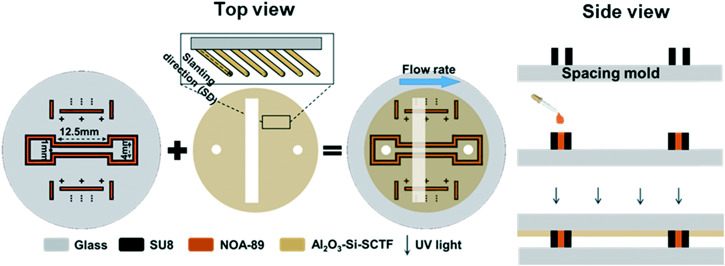 | ||
| Fig. 1 Schematic of glass microfluidic chip fabrication with embedded Al2O3–Si-SCTF using photo lithography, glancing angle deposition technique (GLAD), atomic layer deposition technique (ALD), and nano-plotting. | ||
To make the spacing mold, Omni coat (MicroChem Co., Westborough, MA) was first spin-coated onto a circular glass substrate (with a 31.75 mm diameter and 1.5 mm thickness) at 3000 rpm for 30 s. This process can improve adhesion between the glass substrate and SU8-5 photoresist, which is needed in the next step. The sample was then baked at 200 °C for 1 min. To achieve a thickness of 14 μm, SU8-5 (MicroChem Co., Westborough, MA) was then spin-coated at 1300 rpm for 30 s on the glass substrate covered with Omni coat, then soft-baked for 2 min at 65 °C followed by 5 min at 95 °C. The glass substrate with a SU8-5 cover was then exposed to UV for 13 s using an exposure tool. Following exposure, a post-bake of 1 min at 65 °C and 2 min at 95 °C were performed to cross-link the exposed area of the film. Finally, the designed structure was developed in the SU-8 developer for 3 min. The final mold product was then rinsed with isopropyl alcohol (IPA) and dried with nitrogen.
In the second step, the spacing mold was bonded with a glass slide, which has two holes drilled and Al2O3–Si-SCTF grown as discussed in the SCTF preparation section. NOA-89 UV curing glue (Norland Products, Inc. Cranbury, NJ) was nano-plotted between the pore space of SU8-5 using a GeSiM 2.1 nano-plotter (GeSiM Co., Germany). To bring the viscosity of NOA-89 down, a heatable nano-tip manufactured by GeSiM was used at a temperature of 50 °C. To avoid NOA-89 in contact with water in the tubes and the tip of the nano-plotter, 2 μl ethyl methyl ketone and 20 μl of cyclohexanone (Sigma-Aldrich Co., St. Louis, MO) with 15 μl of an air gap in between were aspirated inside the heatable nano-tip. The buffer solutions and the NOA-89 were stored in a cooled microplate at 12 °C to reduce their rate of evaporation. NOA-89 was plotted on 1315 spots along the center line of the pore space with two drops at each location and a distance of 80 μm maintained between two adjacent locations, which ensures that a sufficient amount of glue filled in the space between the SU8-5 molds. Following plotting, the top glass slide with the Al2O3–Si-SCTF was then aligned and pressed on top of the spacing mold, which was then put under UV light for 20 minutes to allow the two parts to bond by NOA89. Note that to achieve the highest intensity change using ACOM, the experimental slanting direction (Fig. 1) of the Al2O3–Si-SCTF sample was set to 45° with respect to the flow direction.
Prior to the experiment, the microfluidic channel was oxygen-plasma cleaned inside the ALD chamber at 70 °C to remove any remaining residual NOA-89 evaporated on the surface of the Al2O3–Si-SCTF. The inlet and outlet ports of the cleaned and prepared channel were then sealed using Tygon tubes (ID = 0.02′′, OD = 0.06′′) (eMurdock Co.).
2.4. ACOM measurement and GE analysis
ACOM can detect ultra-small amounts of organic as well as inorganic particulates with nanoscopic dimensions based on the optical contrast of an anisotropic filter. Fig. 2a shows a sketch of the ACOM setup. A 100 W short arc mercury lamp provides the light source (S). The light passes through a monochromator (M), a rotating Glan–Thompson polarizer (P), and then the anisotropic and semi-transparent sample of Al2O3–Si-SCTF on glass substrate. In this study, the wavelength of the light was set to 633 nm. An infinity corrected microscope objective (MO) collects light from the sample, which then passes a rotating compensator (C) and another fixed Glan–Thompson polarizer acting as analyzer (A). Finally, a low-noise Photometrics Evolve 512 Delta CCD camera gathers the intensity pictures. Detailed information of the instrument, its calibration and operation can be found in our previous publication.20 In ACOM, the polarizer azimuth (αp) was set to rotate 1° at each step while the compensator azimuth setting was rotating three times faster (αc = 3αp). A total of 360 different intensity images (Fig. 2b), each having 512 by 512 pixel points, were then captured by the CCD camera during the rotation scan. The volumetric fraction of the deposited TiO2NP (fTiO2) on the SCTF layer for each pixel of the intensity image was obtained by best-matching model calculations of the intensity data (ID) using an optical ellipsometry-based anisotropic Bruggeman effective medium approximation (AB-EMA) model,32 as briefly described below. | ||
| Fig. 2 Schematic of the a) anisotropic contrast optical microscope (ACOM). The polarization state generator consists here of a linear polarizer, the polarization state analyzer consists of a half-wave plate and a linear polarizer.20 b-1) ACOM intensity images at selected polarizer azimuth (αp) of 8°, 39°, 272°, and 353° of Al2O3–Si-SCTF inside an ‘N’-shape area for sample ‘Test 1-3’ with piezo-electrically printed nano-liter-sized volumes of nanoparticle solution and b-2) a single-pixel ACOM intensity data (ID) for 360 polarizer azimuth positions of αp. c-1) ACOM intensity images at selected polarizer azimuth (αp) of 32°, 272° of Al2O3–Si-SCTF inside a microfluidic channel ‘Test 2-3’ with TiO2NP deposited on it and b-2) a single-pixel ACOM intensity data (ID) for 360 polarizer azimuth positions of αp. The specimen (TiO2NPs) attachment on anisotropic filter can be measured using ACOM. The hypothetical pixel positions are indicated in the ACOM images by a red square, which is drawn approximately 10 times larger than the pixel size. For further details of the ACOM instrument see Peev et al.20 | ||
The AB-EMA models of the Al2O3–Si-SCTF in the air ambient and Al2O3–Si-SCTF in the microfluidic channel (water ambient) are represented in Fig. 3. In the air ambient, two stratified optical layers, i.e., an anisotropic model layer (AB-EMA) representing the Si-SCTF layer on top of an isotropic glass (substrate) model layer with the refractive index of BK7 (Fig. 3a),33 were considered. In the microfluidic channel (Fig. 3b), four stratified layers, i.e., an isotropic glass layer (optical constants of BK7), an AB-EMA layer of the anisotropic Al2O3–Si-SCTF, an isotropic 14 μm layer of water (water optical properties), and another isotropic glass layer (optical constants of BK7), were included. The optical effect of the 4 nm conformal alumina layer was included by finding effective optical constants for the alumina-coated Si columns prior to the TiO2NP deposition experiment.23 The structural and optical properties of Al2O3–Si-SCTF using the ABM-EMA layer was described by parameters including SCTF thickness (H), slanting angle (θ), slating plane azimuth relative to the linear polarization direction of the fixed analyzer azimuth (Φ), non-spherical depolarization parameters (qz, and splitxy), and the volumetric fraction of constituents (fSi, fambinet).23,28,34 Here, depolarization factors (qz, qx, qy) along the z, x, and y major optical polarizability axes of the SCTF are representative for the relative dimensions of equivalent elliptical inclusions.32,35 The anisotropic optical properties of the Al2O3–Si-SCTF model layer are then described by three dielectric functions, which correspond to the three major optical polarizability axes. Considering m constituent materials, the AB-EMA equation is as follow:
 | (1-1) |
 | (1-2) |
| ε = N2 = (η + iκ)2, | (1-3) |
| qx = (1 − qz) × splitxy, | (2-1) |
| qx + qy + qz = 1, | (2-2) |
| ΓTiO2 = fTiO2 × H × ρTiO2 | (3) |
Here, ρTiO2 is the density of TiO2NPs (3.9 g ml−1).20
 | ||
| Fig. 3 Schematic of the AB-EMA ellipsometry model for Al2O3–Si-SCTF on a) glass substrate in air ambient with TiO2NP attached on its surface and b) inside microfluidic channel in water ambient with TiO2NP attached on its surface used in the analysis of the ACOM images. | ||
When TiO2NP attach on the surface of Al2O3–Si-SCTF, whether on top or deep down on SCTF posts, ACOM detects the change in the optical properties of the posts, and proper AB-EMA model quantifies the overall deposited TiO2NP on Al2O3–Si-SCTF surface. AB-EMA model is based on a homogenization concept. It assumes a well-mixed SCTF, water and attached particle system for each individual pixel point. Based on the homogenization concept, and the fact that the Al2O3–Si-SCTF are semi-transparent to the incoming polarized light, this technique can identify the amount of TiO2NP attachment at a single pixel point on the X–Y plane of Al2O3–Si-SCTF, including both TiO2NP deposited deep inside the spaces between the posts and those deposited closer to the surface of SCTF.
2.5. Sensing experiments in air ambient
Three ‘N’-shape samples (Fig. 4) were prepared to detect TiO2NP in air ambient (test 1-1, test 1-2, test 1-3). For test 1-1 and test 1-2, respectively, 12 locations along the center line of the ‘N’-shape Al2O3–Si-SCTF were printed with sonicated 750 ppm and 1500 ppm TiO2NP solutions twice, that is, every location on the center line received 2 drops, where the distance between each drop location along the center line was maintained to be 125 μm. For tests 1-3, four drops of 1500 ppm TiO2NP solution were printed at each location. A stroboscope camera image analysis was performed within the nano-plotter instrumentation, and the average volumes of the drops were determined as 0.65 nL, 0.66 nL, and 1 nL for test 1-1, test 1-2, and test 1-3, respectively. The total mass of TiO2NP printed thereby for test 1-1, test 1-2, and test 1-3 were estimated as 12 ng, 24 ng, and 72 ng, respectively, based on the total printed volumes and the TiO2NP solution concentrations. After the piezoelectric printing step, the sample was left to dry for 30 minutes before taking intensity images using the ACOM instrument. | ||
| Fig. 4 a) Schematic of locations for controlled piezoelectric printing of nano-liter-sized volumes of TiO2NP solution within a Al2O3–Si-SCTF ‘N’-shape. b) Top-view and high-resolution cross-section electron microscope images of the Al2O3–Si-SCTF. | ||
Properties of the Al2O3–Si-SCTF, including thickness (H), slanting angle (θ), slanting plane azimuth relative to the linear polarization direction of the fixed analyzer azimuth (Φ), fraction of constituents (fSi, fair), depolarization factors (qz, splitxy), and plotted TiO2NP on Al2O3–Si-SCTF surface (fTiO2), were estimated by best matching the ACOM recorded intensity data using a proper GE model, as explained above in the ACOM measurement GE analysis section.
2.6. Sensing experiments under flow conditions
Rotation scan characterization by ACOM is needed to find the initial properties of Al2O3–Si-SCTF (H, θ, Φ, fSi, fwater, qz, splitxy) in water ambient. First, to obtain to the baseline before nanoparticle injection, a single ID was dynamically measured over the entire SCTF area with fixed αp and αc while water was flowing inside the microfluidic channel. The microfluidic channel filled with water was placed in the ACOM with fixed polarizer and compensator azimuth settings (αp and αc) relative to the fix analyzer azimuth, such that the SCTF surface brightened while the glass surface darkened (Fig. 2c-1) (Table 2). Then, the averaged ID was recorded as a single data point over the entire SCTF surface and throughout the experiment. Once the averaged change in the normalized intensity data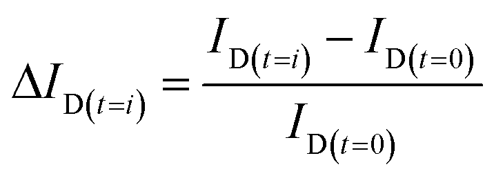 over the entire SCTF pixel points was less than 0.001 h−1, rotation scan characterization was performed. Properties of the Al2O3–Si-SCTF (H, θ, Φ, fSi, fwater, qz, splitxy) were estimated by best matching the ACOM recorded intensity data using a proper GE model. The dynamic measurement was then again set to start by fixing αc and αp to the previous values (Table 2). After several minutes of water introduction into the microfluidic channel, 50 ppm TiO2NP in water solution was introduced into the channel at a flow rate of either 15 μl min−1 or 50 μl min−1. Changes in the single normalized intensity data (ΔID(t)) over the duration of the experiments were instantly recorded while TiO2NP solution was flowing inside the channel. TiO2NP was introduced into the channel for 270 min and 81 min for the experiments at a flow rate of 15 μl min−1 (test 2-1 and test 2-2) and 50 μl min−1 (test 2-3 and test 2-4), respectively, to ensure that an equal mass of TiO2NPs was introduced into the channel in the two experiments. After dynamic measurement was completed, another set of rotation scans was conducted to find the areal mass density distribution of TiO2NPs on the SCTF surface for each pixel point.
Using the AB-EMA model, changes of ID over time for a fixed value of αp and αc were best matched to the ACOM intensity data. The deposition of TiO2NP over the entire SCTF surface with known SCTF properties (H, θ, Φ, fSi, fwater, qz, splitxy) was calculated using the single intensity data over time. However, during the rotation scan (αc = 3αp), 360 different intensity data were measured for each pixel point by ACOM. The AB-EMA model was used on each pixel point to find fTiO2, which best matched the 360 intensity data points measured by ACOM (Fig. 2 and 3).
2.7. Computational fluid dynamic modeling of flow in SCTF
The computational fluid dynamic (CFD) package in COMSOL Multiphysics software (version 4.4) was used to simulate the flow field between SCTF posts at flow rates of 15 μl min−1 and 50 μl min−1. In this simulation, the Navier–Stokes equation was coupled with the continuity equation to obtain a flow velocity field. A constant flow rate boundary condition of 15 μl min−1 or 50 μl min−1 was applied at the inlet boundary, and a zero pressure boundary condition was applied at the outlet boundary. An extremely fine mesh was used to discretize the domain. A fully coupled direct solver was selected for numerical calculation.3. Results and discussion
3.1. TiO2NP and Al2O3–Si-SCTF surface characterization
The zeta potentials of the 1500 ppm and 50 ppm TiO2NP in water solution were −26.9 ± 2.5 mV and −16.5 ± 3.4 mV, respectively. Fig. 5 depicts that hydrodynamic diameter distributions of 1500 ppm and 50 ppm TiO2NP in water were between 1 and 50 nm. Because the average space between individual columns of the Al2O3–Si-SCTF was about 50 nm (Fig. 4b), we expected that majority of TiO2NPs, particularly those with smaller sizes, can penetrate and potentially deposit within the porous structures. | ||
| Fig. 5 Hydrodynamic diameter of TiO2NP in a) 1500 ppm and b) 50 ppm water solution. | ||
The structural parameters of Al2O3–Si-SCTF (H, θ, Φ, qz, splitxy, fSi, and fambient) prior to TiO2NP exposure were estimated using the AB-EMA model (Fig. 3), as provided in Tables 1 and 2 for air and water ambient conditions, respectively. The best match modeled parameters generally agreed with the nominal growth parameters. Particularly, the SCTF thickness (H) was in the range of 430 to 511 nm for all the experiments, which is consistent with the intended thickness of 500 nm. The slanting angle of all experiments ranged from 51 to 67°, which is also consistent with the intended slanting angle of 60°. Both parameters are generally in agreement with the SEM image analysis (Fig. 4b). The small variation among experiments can be attributed to small variations of experimental conditions across the deposited area. The model calculated azimuth orientation of the column slanting plane relative to the linear polarization direction of the fixed analyzer azimuth (Φ) was also consistent with the experimental slanting direction during the imaging experiment. Φ was set at 0° for test 1-1 and test 1-3, and at 45° for test 1-2. We note that the structural parameters of Al2O3–Si-SCTF estimated by the best-matched model were not sensitive to the choice of Φ.
| Parameters | Test 1-1 | Test 1-2 | Test 1-3 |
|---|---|---|---|
| H [nm] | 504 ± 33 | 430 ± 17 | 447 ± 17 |
| θ [°] | 62 ± 2 | 67 ± 1 | 66 ± 1 |
| Φ [°] | −0.3 ± 0.2 | 45.6 ± 0.3 | −0.8 ± 0.2 |
| q z | 0.17 ± 0.01 | 0.17 ± 0.02 | 0.17 ± 0.03 |
| splitxy | 0.37 ± 0.02 | 0.38 ± 0.08 | 0.41 ± 0.04 |
| f Si [%] | 25 ± 2 | 27 ± 2 | 27 ± 2 |
| f air [%] | 75 ± 2 | 73 ± 2 | 73 ± 2 |
| Total NP mass ACOM mMassTiO2NP [ng] | 21 ± 9 | 15 ± 5 | 63 ± 5 |
| Total NP mass print eMassTiO2NP [ng] | 12 ± 1 | 24 ± 2 | 72 ± 1 |
| Parameters | Test 2-1 | Test 2-2 | Test 2-3 | Test 2-4 |
|---|---|---|---|---|
| Flow rate = 15 [μl min−1] | Flow rate = 15 [μl min−1] | Flow rate = 50 [μl min−1] | Flow rate = 50 [μl min−1] | |
| H [nm] | 494 ± 9 | 478 ± 5 | 492 ± 10 | 511 ± 7 |
| θ [°] | 51 ± 1 | 54 ± 1 | 51 ± 1 | 54 ± 1 |
| Φ [°] | 136 ± 2 | 114 ± 5 | 123 ± 3 | 122 ± 3 |
| q z | 0.21 ± 0.01 | 0.16 ± 0.02 | 0.20 ± 0.01 | 0.16 ± 0.01 |
| splitxy | 0.46 ± 0.02 | 0.42 ± 0.05 | 0.45 ± 0.01 | 0.41 ± 0.05 |
| f Si [%] | 33 ± 2 | 34 ± 1 | 34 ± 1 | 31 ± 1 |
| f water [%] | 67 ± 2 | 66 ± 1 | 66 ± 1 | 69 ± 1 |
| α p [°] | 29 | 29 | 30 | 29 |
| α c [°] | 87 | 87 | 90 | 87 |
Although SCTFs with 500 nm thicknesses were used in this study, this method is applicable for any heights of SCTFs, as long as the SCTF posts are slanted, the hydrodynamic size of nanoparticles is smaller than the height of SCTFs and the spacing between SCTFs posts. The size of SCTFs used in this study is in the same range of surface roughness of natural sand grains and glass beads. For example, Rasmuson et al.37 represented environmental surfaces by creating roughness on glass. They have reported that for untreated, NaOH-treated, and HF-treated glass slides, the root-mean square surface roughness measured by AFM were <1 nm, 38 nm, and 546 nm, respectively. Shen et al.38 showed that the AFM measured maximum and the root-mean square surface roughness of 40/60 mesh quartz sand were 2418 nm and 355 nm.38,39
3.2. Sensing TiO2NP in air ambient
Fig. 6a presents typical individual ACOM images of ‘N’-patterned Al2O3–Si-SCTF on glass substrate after nanoparticle exposure under a fixed αp and fixed αc. Based on the GE data analysis approach described above, fTiO2 was estimated for every pixel area A (7 μm × 7 μm). The mass of nanoparticle per pixel, MassTiO2NP, was estimated as (Fig. 6b):| MassTiO2NP = fTiO2 × H × ρTiO2 × A. | (4) |
 | ||
| Fig. 6 Images in rows (a)–(c) pertain to test 1-1, test 1-2, and test 1-3, respectively. Left column: Individual ACOM images of patterned Al2O3–Si-SCTF on glass substrate after nanoparticle exposure; Middle column: images of nanoparticle mass distribution. The scale bars also depict the numerical quantities for nanoparticle number distribution across the SCTF surface (see text); Third column: images of numerical uncertainty of nanoparticle mass and number distributions. d) Comparison of total integrated mass of TiO2NP printed by nanoplotter (‘Experiment’) and total integrated mass obtained from the ACOM image analysis (‘Model’). The error bars correspond to the 90% confidence interval. The ellipsometric model includes the glass slide and the AB-EMA model layer for the anisotropic Si-SCTF surface (field of view: 3.73 mm × 3.73 mm, presented area: 1.74 mm × 1.74 mm, resolution: 7 μm × 7 μm sample surface area imaged per pixel; λ = 633 nm). | ||
The corresponding number quantities of nanoparticles per pixel (noted on the color bar) was also estimated for each pixel by assuming an average mass of approximately 11 attograms per nanoparticle with 17.8 nm in diameter.
Mass distribution images (Fig. 6b) clearly delineate the areas where TiO2NPs were deposited, with non-uniform distributions of TiO2NP mass in the SCTF area. For the experiments with more TiO2NP printed, the ACOM images showed overall higher mass of TiO2NP in the printed area. Test 1-3, the experiment with the highest exposure to nanoparticles, revealed the largest accumulation of mass and more spread of nanoparticles during the evaporation process. A clearly visible coffee stain effect emerged with increasing TiO2NP exposure, revealing a higher concentration of nanoparticles close to the edge of droplets due to the water evaporation process. The average value of the parameter uncertainty for mass, δMass, and accordingly, δnumber, over the observed image area were also provided (Fig. 6) for all three tests. The total masses of nanoparticles estimated by integrating the ACOM mass distribution images were 21 ng, 15 ng, and 63 ng for test 1-1, test 1-2, and test 1-3, respectively, which compared reasonably with the total mass of printed nanoparticles of 12 ng, 24 ng, and 72 ng, respectively (Table 1, Fig. 6d). In all tests, the ACOM estimated mass is within the margin of error of the total nanoplotted mass. Fig. 6d illustrates that this technique is capable to detect trivial amount of TiO2NP mass reasonably well.
We note here that the structural and optical parameters were assumed to be constant over the image area in our analysis. However, local variations in SCTF properties as well as local defects in SCTF coverage always exist, which contributed to the observed deviations between the total printed and total measured mass values, as well as uncertainties of estimated mass (δMass) per pixel. For mass distribution images (Fig. 6a and b), spurious red pixels were observed along some boundaries of the ‘N’-shape SCTF. This artifact can be attributed to the GE analysis errors caused by boundary pixels that partially contain bare glass and SCTF surfaces. For these boundary pixels, the structural and optical parameters for Al2O3–Si-SCTF that were used in the AB-EMA model did not reflect the actual properties of those pixel points. Therefore, the mass distribution of TiO2NP on the Al2O3–Si-SCTF surface is artificial along these edges. Because the deposition of the TiO2NP solution was performed along the center line of the ‘N’-shape Al2O3–Si-SCTF area, the masses calculated based on GE analysis around the edge of the SCTF areas are disregarded in our further analysis. For test 1-2 and 1-3 with a higher mass load, we also note the possibility that small portions of the nanoparticle solution may have flown outside the SCTF areas prior to solvent evaporation, thereby transporting small fractions of nanoparticles onto the optically isotropic glass surface. Nanoparticles residing in the bare glass surface areas are undetectable to ACOM, which partially explains the fact that the model slightly underestimated the mass (Fig. 6d) for tests 1-2 and 1-3.
The demonstrated capability of sensing nanoparticles on a highly ordered columnar nanostructured surface in air ambient is unprecedented. We were able to detect a few picograms of nanoparticles (17.8 nm in diameter) within a sample surface area of approximately 7 μm × 7 μm without the help of any labeling technique. In addition to mass distribution images, we have demonstrated a reasonably accurate quantitative capability of the technique (Fig. 6d). The sensing capability demonstrated here is better than the currently prevalent particle sensing instrumentation, for example, QCM-D. Although QCM-D can dynamically measure the overall mass of nanoparticles attached on its surface,40,41 it cannot quantify the distribution of the attached nanoparticles on the sensor surface.
3.3. Sensing TiO2NPs under flow condition
Based on the intensity change captured by ACOM, the AB-EMA model can be used to estimate the areal mass density of TiO2NP attached to the surface of Al2O3–Si-SCTF (ΓTiO2) as TiO2NP was introduced into the microfluidic channel. Fig. 7a and b showed an increase in ΓTiO2 over time while TiO2NP solution was flowing inside the channel. Note that the shaded areas in Fig. 7 correspond to the ACOM detection limit, which was averaged as ±250 ng cm−2 (2.5 fg μm−2). In our previous publication,20 the detection limit for cetyltrimethylammonium bromide (CTAB) was determined as 1 fg μm−2. Because TiO2NPs are larger than CTAB molecules, higher level of random depolarization and scattering will occur when light hits TiO2NPs, which led to larger error bars for the ellipsometry measurement, and therefore, a higher detection limit. The accuracy of this technique depends on the calibration of SCTF surface prior to nanoparticles deposition, which finds proper structural and optical properties of SCTF. Here accuracy was on the same order of magnitude to detection limit, because SCTF surface was calibrated correctly. | ||
| Fig. 7 The areal mass density of the attached TiO2NP on the Al2O3–Si-SCTF surface for the flow rates of a) 15 μl min−1 and b) 50 μl min−1 of 50 ppm TiO2NPs solution. | ||
Repeated experiments were conducted at a lower flow rate of 15 μl min−1 (Fig. 7a) and a higher flow rate of 50 μl min−1 (Fig. 7b). Here, repeated experiments were conducted using two different microfluidic channels with SCTFs embedded. Although the Al2O3–Si-SCTF surface in each channel possesses the same average properties, nanoscale non-uniformities are expected for each individual surface. Because ACOM is very sensitive to any nanoscale attachment, it is expected that two repeated experiments could reproduce similar trends of mass increase but not the exact same amount over time. It should be noted that, the sudden increase and decrease of the areal mass density of attached TiO2NPs for test 2-2 (Fig. 7a) at the initial stage of the experiment was due to the entrance of a bubble into the microfluidic channel, which interfered the intensity measurement. After that, the measurement was back to normal and showed similar trend of TiO2NP attachment as the parallel experiment (test 2-1).
As shown in Fig. 7, ΓTiO2 gradually increased for all the experiments while TiO2NP solution was introduced into the microfluidic channels. After the same amount of TiO2NP mass (i.e., 203 μg) was introduced, ΓTiO2 reached 1837 ± 301 ng cm−2 and 1890 ± 168 ng cm−2 for lower flow rate experiments (i.e., tests 2-1 and 2-2) and 1200 ± 244 ng cm−2 and 920 ± 284 ng cm−2 for higher flow rate experiments (i.e., tests 2-3 and 2-4). The repeated experiments under both flow rates were in close agreement regarding the total amount of TiO2NP mass attached on the SCTFs. The slopes of the mass increase were also consistent between repeated experiments under both flow rates, indicating the reproducibility of the technique. More mass of TiO2NPs were attached to the SCTF surface per mass of TiO2NP introduced into the channel under the lower flow rate than the higher flow rate. This is depicted by the slope of the curves in Fig. 7 and is due to the longer residence time of TiO2NPs in the microfluidic device corresponding to the lower flow rate. The average attached mass rate, defined by the ratio of ΓTiO2 to the injection time, was 6.9 ng cm−2 min for the lower flow rate experiments (test 2-1 and test 2-2) and 14.3 ng cm−2 min for the higher flow rate experiments (test 2-3 and test 2-4).
Fig. 8a shows representative intensity images in the location adjacent to the channel inlet at a fixed αp and fixed αc setting (depicted in Table 2) before introducing TiO2NP solution into the microfluidic channel. Fig. 8b depicts the corresponding distribution of attached TiO2NP on the Al2O3–Si-SCTF surface at the end of the experiment, at each individual pixel point, with color scale bars in terms of mass density (ΓTiO2), mass of TiO2NP per pixel (MassTiO2), and the number of TiO2NP per pixel (NTiO2). Here, MassTiO2 was calculated by multiplying ΓTiO2 with the area of each individual pixel point. NTiO2 was also calculated from the mass of an individual TiO2NP assuming an average hydrodynamic diameter of 24 nm (Fig. 5b). Fig. 8c represents the example comparison between the ACOM experimental intensity measurement and AB-EMA best-matched ID scaled by the measured maximum ID data (SID) for each test at a selected individual pixel. The R-squared values for all best-matched single pixel points were higher than 0.9.
 | ||
| Fig. 8 a) ACOM intensity images at selected polarizer azimuth settings (refer to Table 2). b) Distribution of areal mass density, mass, and number of attached TiO2NP on Al2O3–Si-SCTF surface (ΓTiO2) for each individual pixel. c) ACOM measured and AB-EMA best-matched scaled intensity data (SID) using ACOM and AB-EMA model respectively for one pixel point (R2 = 0.99). | ||
Distributions of TiO2NP were not uniform on the surface of Al2O3–Si-SCTF for each individual test. Some pixel points showed more particles while others showed less or no TiO2NP. The spatial distribution of TiO2NP on the Al2O3–Si-SCTF surface was not expected to be the same between repeated experiments (test 2-1 and 2-2; test 2-3 and 2-4) due to the nanoscale non-uniformities on the surface of Al2O3–Si-SCTF as explained earlier and shown in Fig. 8a. However, the overall attachments revealed by integrating the particle mass on the area were consistent between each repeated experiment. The averaged ΓTiO2 for the entire area of Al2O3–Si-SCTF based on the ΓTiO2 distribution (Fig. 8b) were 1183 ng cm−2, 1778 ng cm−2, 1293 ng cm−2, and 968 ng cm−2 for test 2-1, test 2-2, test 2-3, and test 2-4, respectively. Most importantly, the averaged ΓTiO2 estimated based on Fig. 8b had good agreement with the dynamic measurement of ΓTiO2, as depicted in Fig. 9. Two approaches estimated a similar average mass density of TiO2NP at the end of the experiments, which further demonstrates the ability of this sensing technique to quantitatively determine the areal mass density of nanoparticles on a SCTF surface (Fig. 9).
 | ||
| Fig. 9 Areal mass density of attached TiO2NP on SCTF surface inside microfluidic channel calculated based on dynamic measurement (fixed αp and αc), and the rotation scan data (αc = 3αp). | ||
Comparing experiments under different flow rates, more TiO2NPs were attached under the lower flow rate, although the attached mass rate was higher for the higher flow rates. Fig. 10 presents the CFD simulated flow velocity distribution inside SCTF under flow rates of 15 and 50 μl min−1. The Reynolds numbers for flow in between SCTF posts and at a SCTF scale were estimated as 4.33 × 10⁻⁵ and 1.5 × 10⁻³ for flow rates of 15 and 50 μl min−1, respectively, considering an SCTF characteristic length of 870 nm and the average velocity between two SCTF posts. As both flow conditions are laminar, TiO2NP nanoparticles need to come across the flow streamlines to approach the surface of SCTF. For nanoparticles measuring 24 nm in diameter, diffusion is the dominating mechanism for attachment. Nanoparticles would easier come across flow streamline under the higher flow rate where a sharper velocity gradient exists adjacent to the SCTF surface. Although the surface charges of Al2O3–Si-SCTFs were not measured in our study, Gu et al.42 calculated a positive charge of 25 mV for the thin ALD layer of alumina on a silicon wafer at pH 7 in 1 mM KCl solution, which is close to our condition. Once nanoparticles diffuse across the streamlines, a favorable attachment is expected to occur between negatively charged TiO2NP and positively charged Al2O3–Si-SCTF based on DLVO interaction theory.43 Therefore, a higher attached mass rate under a higher flow rate is expected. The lower flow rate, however, allows longer residence time of nanoparticles inside SCTFs, so eventually more nanoparticles can diffuse across the flow streamlines and get closer to the SCTF surface. Hence, a higher retention amount of TiO2NP corresponds to the same mass of TiO2NP introduced into the microfluidic channel under a lower flow rate than a higher flow rate.
 | ||
| Fig. 10 Velocity distributions between SCTF posts for the flowrates of a) 15 μl min−1, and b) 50 μl min−1. | ||
4. Conclusions
In summary, we demonstrated an innovative technique to visualize and quantify the deposition of non-labeled TiO2NP with a diameter smaller than 50 nm on model Al2O3–Si-SCTF rough surfaces in air and under flow conditions using ACOM. We first demonstrated the capability of using ACOM and the appropriate optical model to measure the distribution of TiO2NP on the SCTF rough surface by dropping a known amount of TiO2NP onto the surface. We found reasonable agreement between the ACOM measured and dropped mass of TiO2NPs. Detection of a few picograms of nanoparticle mass by an individual pixel of 7 × 7 μm2 was presented. We then applied the same technique to measure and visualize the attachment of label-free TiO2NP on an engineered 500 nm-thick Al2O3–Si-SCTF surface inside glass microfluidic channels at two different flow rates. We demonstrated the ability to instantly measure the deposition of TiO2NP on these surfaces during the introduction of TiO2NP into the microfluidic channel. During the introduction of 203 μg of TiO2NP, the averaged attached TiO2NP mass density on the Al2O3–Si-SCTF surface was 1.6-fold higher at a flow rate of 15 μl min−1 compared to 50 μl min−1. However, the deposition rate was higher under a higher flow rate, which was expected and reasonable based on flow simulation. We were able to visualize the distribution of the attached TiO2NP on the Al2O3–Si-SCTF surface at the end of the TiO2NP solution introduction into the microfluidic channel. Although the detailed distribution map of TiO2NP was different between experiments due to nanoscale non-uniformities, the averaged mass density estimated by integrating the distribution map was in close agreement with the estimation from dynamic measurements and between repeated experiments.By implementing the ACOM instrument with the proper optical model, we were able to visualize and quantify the distribution of TiO2NP on the SCTF surface under both static and flow conditions. This technique can be applied to any type of nanoparticles with hydrodynamic sizes smaller than the height and spaces between SCTF posts, given the optical properties of nanoparticles (i.e. refractive index, extinction coefficient) are known. Technically it is possible to manufacture SCTF with different dimensions; therefore, this method can be applicable to a wide range of nanoparticles or the mixture of nanoparticles, although it cannot differentiate between different types of nanoparticles. As proof-of-concept, experiments in this study was conducted with simple water chemistry. The method is applicable to more environmentally relevant water condition with various dissolved ions present. If water contains solutes that may attach to the surface of SCTF, e.g. natural organic matter, the technique is also applicable but requires an additional calibration step to quantify the attachment of the additional solutes on SCTF surfaces. In addition, by manipulating the physical and chemical properties of SCTF surfaces, for example covering the part of the SCTF surfaces with natural organic matters (NOM) using lithography technique, this technique will provide an innovative avenue to investigate interaction of label-free ENPs with rough surfaces of various properties.
Conflicts of interest
Authors declare no conflict of interest.Acknowledgements
Support for this research was provided in part by funds from the Center for Nanohybrid Functional Materials (NSF-EPS-10004094), NSF awards CBET- 1133528, CBET- 1521428, and the American Chemical Society Petroleum Research Funds PRF # 59374-ND5. We thank Thomas Wegener and Thomas Gehring form Gesim Co. for their help with the project. The research was performed in part in the Nebraska Nanoscale Facility: National Nanotechnology Coordinated Infrastructure and the Nebraska Center for Materials and Nanoscience, which are supported by the National Science Foundation under Award ECCS: 1542182, and the Nebraska Research Initiative.References
- C. O. Robichaud, A. E. Uyar, M. R. Darby, L. G. Zucker and M. R. Wiesner, Estimates of upper bounds and trends in nano-TiO2 production as a basis for exposure assessment, Environ. Sci. Technol., 2009, 4227–4233 CrossRef CAS.
- A. A. Keller and A. Lazareva, Predicted releases of engineered nanomaterials: from global to regional to local, Environ. Sci. Technol. Lett., 2013, 1(1), 65–70 CrossRef.
- C. M. Mansfield, M. M. Alloy, J. Hamilton, G. F. Verbeck, K. Newton, S. J. Klaine and A. P. Roberts, Photo-induced toxicity of titanium dioxide nanoparticles to Daphnia magna under natural sunlight, Chemosphere, 2015, 120, 206–210 CrossRef CAS PubMed.
- G. Chen, X. Liu and S. Chunming, Transport and Retention of TiO2 Rutile Nanoparticles in Saturated Porous Media under Low-Ionic-Strength Conditions: Measurements and Mechanisms, Langmuir, 2011, 27(9), 5393–5402 CrossRef CAS PubMed.
- G. Chen, X. Liu and C. Su, Distinct Effects of Humic Acid on Transport and Retention of TiO2 Rutile Nanoparticles in Saturated Sand Columns, Environ. Sci. Technol., 2012, 46, 7142–7150 CrossRef CAS PubMed.
- C. C. Choy, M. Wazne and X. G. Meng, Application of an empirical transport model to simulate retention of nanocrystalline titanium dioxide in sand columns, Chemosphere, 2008, 71(9), 1794–1801 CrossRef CAS PubMed.
- S. H. Joo, S. R. Al-Abed and T. Luxton, Influence of Carboxymethyl Cellulose for the Transport of Titanium Dioxide Nanoparticles in Clean Silica and Mineral-Coated Sands, Environ. Sci. Technol., 2009, 43(13), 4954–4959 CrossRef CAS PubMed.
- G. Cornelis, K. Hund-Rinke, T. Kuhlbusch, N. Van den Brink and C. Nickel, Fate and bioavailability of engineered nanoparticles in soils: a review (2014), Crit. Rev. Environ. Sci. Technol., 2014, 44, 2720–2764 CrossRef CAS.
- G. Cornelis, L. Pang, C. Doolette, J. K. Kirby and M. J. McLaughlin, Transport of silver nanoparticles in saturated columns of natural soils, Sci. Total Environ., 2013, 436–464, 120–130 CrossRef PubMed.
- G. Cornelis, C. Doolette, M. Thomas, M. J. McLaughlin, J. K. Kirby, D. G. Beak and D. Chittleborough, Retention and dissolution of engineered silver nanoparticles in natural soils, Soil Sci. Soc. Am. J., 2012, 76, 891–902 CrossRef CAS.
- B. J. R. Thio, D. Zhou and A. A. Keller, Influence of natural organic matter on the aggregation and deposition of titanium dioxide nanoparticles, J. Hazard. Mater., 2011, 189(1–2), 556–563 CrossRef CAS PubMed.
- N. Kananizadeh, C. Rice, J. Lee, K. B. Rodenhausen, D. Sekora, M. Schubert, E. Schubert, S. Bartelt-Hunt and Y. Li, Combined quartz crystal microbalance with dissipation (QCM-D) and generalized ellipsometry (GE) to characterize the deposition of titanium dioxide nanoparticles on model rough surfaces, J. Hazard. Mater., 2017, 322, 118–128 CrossRef CAS PubMed.
- J. Fatisson, R. F. Domingos, K. J. Wilkinson and N. Tufenkji, Deposition of TiO2 nanoparticles onto silica measured using a Quartz Crystal Microbalance with Dissipation monitoring, Langmuir, 2009, 25(11), 6062–6069 CrossRef CAS PubMed.
- K. A. D. Guzman, M. P. Finnegan and J. F. Banfield, Influence of surface potential on aggregation and transport of titania nanoparticles, Environ. Sci. Technol., 2006, 40(24), 7688–7693 CrossRef PubMed.
- Y. Kusaka, J. F. L. Duval and Y. Adachi, Morphology and Breaking of Latex Particle Deposits at a Cylindrical Collector in a Microfluidic Chamber, Environ. Sci. Technol., 2010, 44, 9413–9418 CrossRef CAS PubMed.
- M. R. de Saint Vincent, M. Abkarian and H. Tabuteau, Dynamics of colloid accumulation under flow over porous obstacles, Soft Matter, 2016, 12(4), 1041–1050 RSC.
- M. B. Seymour, G. Chen, C. Su and Y. Li, Transport and Retention of Colloids in Porous Media: Does Shape Really Matter?, Environ. Sci. Technol., 2013, 47(15), 8391–8398 CAS.
- R. May, S. Akbariyeh and Y. S. Li, Pore-Scale investigation of nanoparticle transport in saturated porous media using laser scanning cytometry, Environ. Sci. Technol., 2012, 46(18), 9980–9986 CAS.
- C. Chen, T. Waller and S. L. Walker, Visualization of transport and fate of nano and micro-scale particles in porous media: modeling coupled effects of ionic strength and size, Environ. Sci.: Nano, 2017, 4, 1025–1036 RSC.
- D. Peev, T. Hofmann, N. Kananizadeh, S. Beeram, E. Rodriguez, S. Wimer, B. Rodenhausen, C. M. Herzinger, T. Kasputis and E. Pfaunmiller, et al. Anisotropic contrast optical microscope, Rev. Sci. Instrum., 2016, 87(11), 113701 CrossRef CAS PubMed.
- H. Fujiwara, Spectroscopic Ellipsometry, John Wiley & Sons, New York, 2007 Search PubMed.
- M. Schubert, B. Rheinlander, J. A. Woollam, B. Johs and C. M. Herzinger, Extension of rotating-analyzer ellipsometry to generalized ellipsometry: Determination of the dielectric function tensor from uniaxial TiO2, J. Opt. Soc. Am. A, 1996, 13(4), 875–883 CrossRef CAS.
- N. Kananizadeh, C. Rice, J. Lee, K. B. Rodenhausen, D. Sekora, M. Schubert, E. Schubert, S. Bartelt-Hunt and Y. Li, Combined quartz crystal microbalance with dissipation (QCM-D) and generalized ellipsometry (GE) to characterize the deposition of titanium dioxide nanoparticles on model rough surfaces, J. Hazard. Mater., 2017, 322, 118–128 CrossRef CAS PubMed.
- K. B. Rodenhausen, D. Schmidt, C. Rice, T. Hofmann, E. Schubert and M. Schubert, Detection of organic attachment onto highly ordered three-dimensional nanostructure thin films by generalized ellipsometry and quartz crystal microbalance with dissipation techniques, in Ellipsometry of Functional Organic Surfaces and Films, ed. K. Eichhorn, Springer, Berlin, 2013 Search PubMed.
- D. Schmidt, E. Schubert and M. Schubert, Generalized Ellipsometry Characterization of Sculptured Thin Films Made by Glancing Angle Deposition, in Ellipsometry at the Nanoscale, ed. M. Losurdo and K. Hingerl, Springer, 2013, pp. 341–410 Search PubMed.
- D. Liang, D. Schmidt, H. Wang, E. Schubert and M. Schubert, Generalized ellipsometry effective medium approximation analysis approach for porous slanted columnar thin films infiltrated with polymer, Appl. Phys. Lett., 2013, 103, 11906 CrossRef.
- M. Scubert, Handbook of ellipsometry, ed. H. Tompkins and E. A. Irene, William Andrew, 2005 Search PubMed.
- D. Schmidt, E. Schubert and M. Schubert, Optical properties of cobalt slanted columnar thin films passivated by atomic layer deposition, Appl. Phys. Lett., 2012, 100, 011912 CrossRef.
- M. M. Hawkeye and M. J. Brett, Glancing angle deposition: fabrication, properties, and applications of micro-and nanostructured thin films, J. Vac. Sci. Technol., A, 2007, 25(5), 1317–1335 CrossRef CAS.
- X. Liu, G. Chen and C. Su, Influence of Collector Surface Composition and Water Chemistry on the Deposition of Cerium Dioxide Nanoparticles: QCM-D and Column Experiment Approaches, Environ. Sci. Technol., 2012, 46(12), 6681–6688 CrossRef CAS PubMed.
- A. L. J. Olsson, I. R. Quevedo, D. He, M. Basnet and N. Tufenkji, Using the Quartz Crystal Microbalance with Dissipation Monitoring to Evaluate the Size of Nanoparticles Deposited on Surfaces, ACS Nano, 2013, 7(9), 7833–7843 CrossRef CAS PubMed.
- D. Schmidt and M. Schubert, Anisotropic Bruggeman effective medium approaches for slanted columnar thin films, J. Appl. Phys., 2013, 114(8), 083510 CrossRef.
- E. D. Palik, Handbook of Optical Constants of Solids, Academic Press, New York, 1998 Search PubMed.
- K. B. Rodenhausen, R. S. Davis, D. Sekora, D. Liang, A. Mock, R. Neupane, D. Schmidt, T. Hofmann, E. Schubert and M. Schubert, The retention of liquid by columnar nanostructured surfaces during quartz crystal microbalance measurements and the effects of adsorption thereon, J. Colloid Interface Sci., 2015, 455, 226–235 CrossRef CAS PubMed.
- M. Losurdo and K. Hingerl, Ellipsometry at the nanoscale, Springer Science & Business Media, 2013 Search PubMed.
- M. C. Kuzyk and C. W. Dirk, Characterization techniques and tabulations for organic nonlinear optical materials, Marcel Dekker, Inc., 1998 Search PubMed.
- A. Rasmuson, E. Pazmino, S. Assemi and W. P. Johnson, Contribution of nano- to microscale roghness to heterogeneity: closing the gap between unfavorable and favorable colloid attachment conditions, Environ. Sci. Technol., 2017, 51, 2151–2160 CrossRef CAS PubMed.
- C. Y. Shen, B. G. Li, C. Wang, Y. F. Huang and Y. Jin, Surface roughness effect on deposition of nano- and micro-sized colloids in saturated columns at different solution ionic strengths, Vadose Zone J., 2011, 10(3), 1071–1081 CrossRef CAS.
- S. Torkzaban and S. A. Bradfor, Critical role of surface roughness on colloid retention and release in the porous media, Water Res., 2016, 88, 274–284 CrossRef CAS PubMed.
- J. Fatisson, S. Ghoshal and N. Tufenkji, Deposition of carboxymethylcellulose-coated zero-valent Iron nanoparticles onto silica: Roles of solution chemistry and organic molecules, Langmuir, 2010, 26(15), 12832–12840 CrossRef CAS PubMed.
- B. J. R. Thio, D. Zhou and A. A. Keller, Influence of natural organic matter on the aggregation and deposition of titanium dioxide nanoparticles, J. Hazard. Mater., 2011, 189, 556–563 CrossRef CAS PubMed.
- D. Gu, S. Yalcin, H. Baumgart, S. Qian, O. Baysal and A. Beskok, Electrophoretic Light Scattering for Surface Zeta Potential Measurement of ALD Metal Oxide Films, ECS Trans., 2010, 33(2), 37–41 CAS.
- M. Elimelech, J. Gregory, X. Jia and R. A. Williams, Particle deposition and aggregation: measurement, modeling and simulation, Butterworth-Heinemann: Oxford, England, 1995 Search PubMed.
Footnote |
| † Electronic supplementary information (ESI) available. See DOI: 10.1039/c8en00984h |
| This journal is © The Royal Society of Chemistry 2019 |