
 Open Access Article
 This Open Access Article is licensed under a Creative Commons Attribution-Non Commercial 3.0 Unported Licence
Carbon-based materials for stable, cheaper and large-scale processable perovskite solar cells
Lucia
Fagiolari
 * and
Federico
Bella
*
* and
Federico
Bella
*
GAME Lab, Department of Applied Science and Technology (DISAT), Politecnico di Torino, Corso Duca degli Abruzzi 24, 10129 – Torino, Italy. E-mail: federico.bella@polito.it; lucia.fagiolari@polito.it; Tel: +39 0110904643
First published on 25th October 2019
Abstract
Almost ten years after their first use in the photovoltaic (PV) field, perovskite solar cells (PSCs) are now hybrid devices that, in addition to having reached silicon performance, can accelerate the energy transition and boost the use of abundant elements for their manufacturing process. However, noble metals (in particular gold) represent the most typically used sources for back electrode fabrication, and this issue has been intensively considered by the research community in the last five years. This review shows how the most promising solution, considering also the need to develop a large-scale production process, is based on the use of carbon-based materials for the preparation of back electrodes. Graphite, carbon black, graphene and carbon nanotubes (CNTs) have been proposed, functionalized and characterized, leading to laboratory-scale solar cells and modules capable of providing excellent efficiencies and ensuring stability greater than those of gold-based devices. Strengthened by these results and its hydrophobizing properties, carbon has also started to be used as an electron transporting material (ETM), with excellent results on both rigid and flexible substrates. This review discusses the major advances and the updated state-of-the-art in the carbon-based PSC scenario, keeping a solid trajectory where the accessibility, low cost, high electrical conductivity, chemical stability and controllable porosity of carbon are highlighted and exploited in the design of upscalable hybrid solar cells.
 Lucia Fagiolari | Lucia Fagiolari is a post doc researcher at Politecnico di Torino, Italy. She received her BSc, MSc and PhD in Chemical Sciences from the University of Perugia (Italy). During her PhD, she has been a visiting student at the University of Zurich – Irchel Campus (Switzerland). Currently, her research work concerns the development of dye-sensitized and perovskite solar cells, with a focus on the use of renewable raw materials and preparation processes under ambient conditions. She was awarded with the best poster prize at the 19th International Symposium on Intercalation Compounds. She is the author of 2 publications in international peer-reviewed journals (h-index = 2). |
 Federico Bella | Federico Bella is an assistant professor of Chemistry at Politecnico di Torino (Italy). He received both BSc and MSc in Industrial Chemistry from the University of Turin (Italy) and PhD in Electronic Devices from the Italian Institute of Technology. He has been a visiting scientist at Universitat Politècnica de València, National University of Malaysia, École Polytechnique Fédérale de Lausanne and Massachusetts Institute of Technology. Currently, he is working in the field of solar cells and secondary batteries, focusing on stable electrolytes and chemometric approaches. He has recently been awarded with the RSC “Environment, Sustainability & Energy Division Early Career Award” and with the international “Roberto Piontelli” award 2019 by the Accademia Nazionale dei Lincei, one of the oldest scientific institutions in the world. He is the author of 70 publications in international peer-reviewed journals (h-index = 44), and he is the former coordinator of the Young Division of the Italian Chemical Society. |
Broader contextToday, more than 75% of the world energy demand is met by traditional, non-sustainable energy resources, mainly based on coal, natural gas and oil. Photovoltaics represents a concrete action to mitigate fossil fuel consumption, and among all the developed solar cells, perovskite-based ones have shown the highest increase in terms of efficiency (currently above 25%). Halide perovskites, as a family of new-generation semiconductor materials, are also exploitable for light-emitting devices, photodetectors and memristors, but their use in photovoltaics gives rise to outstanding performances. Here, photogenerated charges pass through electron/hole transporting materials and are transferred to the external circuit by front and back electrodes. While the front electrode is a common conductive glass, many issues are now under study concerning the back electrode, traditionally made of gold. Indeed, replacing this expensive metal with a much cheaper alternative is vital for realizing affordable solar technologies. Carbon, in its multiple forms, represents the winning solution and the scientific community has recently shown its large scale processability, its power as a stability booster and some interesting effects at the perovskite/electrode interface. This review shows how carbon is becoming the winning ingredient for the scaling up and worldwide diffusion of perovskite solar cells. |
1 Introduction
Among all PV fields, PSCs have shown the highest increase in terms of power conversion efficiency (PCE), passing from 3.8%1 to 25.2%2 in just a few years.3–7 Perovskites are materials with the generic formula ABX3, where A is an organic larger cation, situated in the eight corners of the unit cell, with cubo-octahedral coordination, B is a metal cation located at the body center, and X represents an anion that binds them both.8,9 This kind of material has attracted much attention, due to its superb characteristics, such as strong and broad optical absorption from the visible to the near-infrared (NIR) range,10 long carrier lifetime, long diffusion length (from 100 nm to 1 μm), a direct optical band-gap of 1.5 eV and low exciton binding energy.11–13 In addition, these semiconductors offer good versatility and processability from solution.14,15 In PSCs, perovskites are used as light absorber and charge transporting materials.16–18 One of the most commonly used perovskites is the hybrid organic–inorganic compound, CH3NH3PbI3.19–21One of the main drawbacks toward the commercialization of PSCs is the use of noble metals, such as gold and silver, as back electrodes, thus limiting their large-scale application. Gold and silver are expensive rare metals and their deposition requires a highly energy-consuming vacuum evaporation method.22 In addition, silver and gold electrodes may deteriorate cell performance,23 due to migration of halogen atoms from the perovskite phase, with formation of silver and gold halides.24–26
The most common carbon-based materials used in the PSC field are graphite/amorphous carbon, graphene, and CNTs. They represent a suitable solution to substitute noble metals, due to their low cost, high conductivity, eventual low-temperature processing (100 °C)1,27,28 and work function close to that of gold (5.0 and 5.1 eV, respectively).29,30 Another advantage of carbon-based components reflects on perovskite degradation in the presence of water, that leads to the formation of the hydrated phases CH3NH3PbI3·H2O and (CH3NH3)4PbI6·2H2O;31 while the formation of the monohydrate phase is reversible, the dihydrate phase degrades irreversibly to yellow PbI2 and CH3NH3I.32 Conversely, carbon-based materials can improve PSC stability due to their highly hydrophobic nature that leads to the prevention of moisture penetration in the perovskite layer, even without carrying out the sealing process.24
Nonetheless, carbon-based materials also present many drawbacks, associated especially with their processability on a large scale. For example, graphene, the 2D layer of graphite, is a very versatile material with metal-like properties; however, it is difficult to be obtained by mechanical or chemical exfoliation on a large scale. The dispersion of graphene layers from graphite requires a large amount of organic solvents, such as dimethylformamide; on the other hand, the epitaxial growth on SiC by vacuum graphitization has the disadvantages of high temperature (1300 °C) and high costs of the monocrystalline SiC sheet.33,34 Chemical vapour deposition (CVD) is more applicable on a large scale, but has hardly any control on film thickness and requires expensive substrates (Ni, Cu, Pd, Pt).35 CNTs are composed of graphitic layers rolled up to form a cylinder. For this reason, in each tube, an elevated charge-transfer resistance is created.34,36 The problem is partially solved by the use of multi-walled CNTs (MWCNTs), which consist of multiple CNTs stacked together.
In some cases reported in this review, graphite and amorphous carbon require a high processing temperature. They form a rigid structure that impedes the penetration of the perovskite precursor solution. For this reason, the use of carbon black (CB) is necessary to break the oriented and impermeable graphite layer. In addition, in most cases, the small CB nanoparticles are obtained by the incomplete combustion of fossil fuels.
This review focuses on the current trends and major achievements obtained from hundreds of research teams working on carbon-based PSCs.37 From our analysis of literature databases, it clearly emerges that graphite and CB represent the most credible realities if the target is – in a short time – a printable and industrially scalable solar energy conversion technology. We will show how the strategies for functionalizing and engineering the interfaces between carbon and perovskites or carbon and hole transporting materials (HTMs) strongly influence the cell PCE and stability. Finally, we will offer an overview of the state of the art of alternative carbon-based materials, such as CNTs and graphene, that show interesting aspects when low temperature processes or flexible device fabrications are envisaged. The achievement of stable, cheap and reproducible PSCs will be fundamental in view of their worldwide diffusion in the energy scenario, as well as integration with energy storage technologies.38–47
2 Graphite- and carbon black-based back electrodes
Generally speaking, a PSC is based on a perovskite layer48,49 sandwiched between an ETM and a HTM.50,51 The ETM usually consists of TiO2 or another n-type semiconductor anode,52–54 while the back electrode is deposited on top of the HTM.55–57 For efficient charge extraction, the valence band (VB) and the conduction band of the perovskite should lie below the highest occupied molecular orbital (HOMO) of the HTM and under the lowest unoccupied molecular orbital (LUMO) of the ETM, respectively.58,59 After light absorption, in the perovskite layer an electron–hole pair is generated.60,61 Electrons are collected by the ETM and migrate towards the anode side, while holes are collected by the HTM and migrate towards the back electrode. The most common organic HTMs are expensive and require an inert atmosphere for the deposition process.62–64 They are also subjected to halide and metal ion migration,65 resulting in the degradation of the cell.66–68 2,2,7,7-tetrakis(N,N-di-p-methoxyphenylamine)-9,9′-spirobifluorene (spiro-OMeTAD) is commonly used as a HTM in gold-based PSCs.69 It needs to be doped with lithium bis(trifluoromethanesulfonyl)imide (LiTFSI), a hygroscopic and deliquescent salt that allows the penetration of water molecules, leading to the decomposition of the perovskite.70,71 Luckily, perovskite materials show a large carrier path and PSCs can also work without the HTM.72,73 In this architecture, an insulating layer, such as Al2O3 or ZrO2, is necessary to keep the front electrode separated from the back one.74To date, the best performances have been obtained with gold as the back electrode. However, the noble element may be replaced by carbon-based materials, such as graphite, graphene, CNTs and so on. In fact, carbon has a suitable work function of 5.0 eV, very close to that of gold (5.1 eV).29 In addition, carbon-based materials are processable, highly conductive, thermally inert and hydrophobic.75 Carbon-based back electrodes represent a concrete and indispensable strategy towards the large-scale industrial production of PSCs. Fig. 1 shows that it took 4 years, from the first reported perovskite-based PVs (2009), to see the first articles published on this topic. However, it must also be specified that all articles on PSCs published before 2012 were focused on devices using liquid electrolytes. Carbon-based devices appeared approximately only one year after the first solid-state PSC based on spiro-OMeTAD. As well known, the unexpected efficiency improvement that spiro-OMeTAD promoted is sometimes considered the true starting point of the PSC topic. To date, publications on carbon-based PSCs count for about 10% of the overall PSC articles, maintaining an upward trend after 2015.
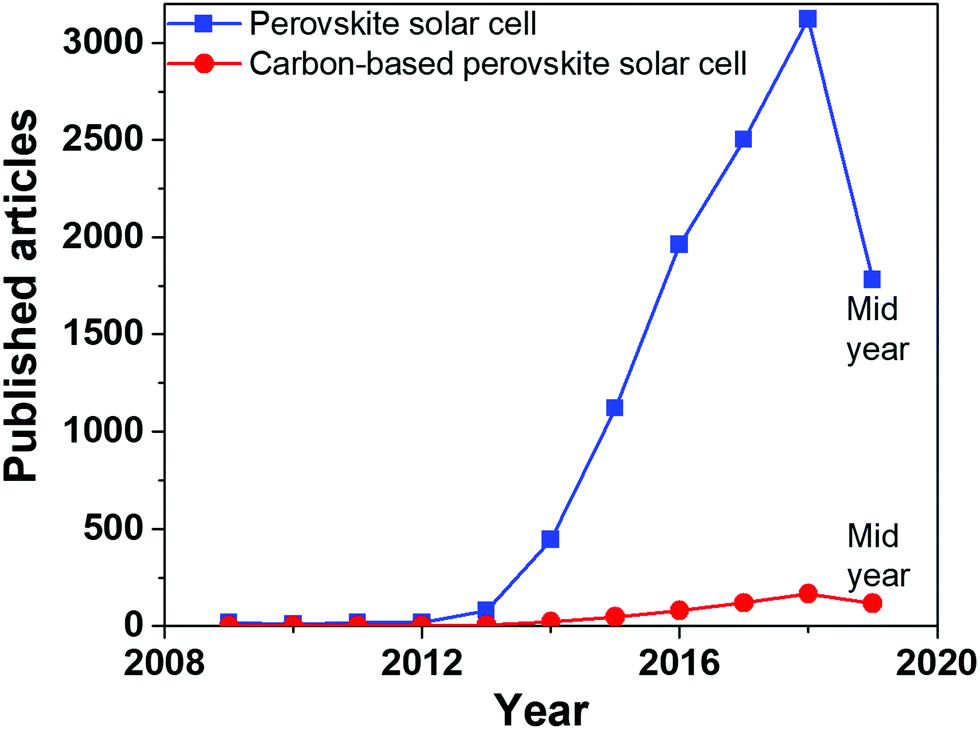 | ||
| Fig. 1 Published articles from 2009 to 2019 on “perovskite solar cells” and “carbon-based perovskite solar cells”. Data extracted from Scopus database on 30th June 2019. | ||
Among the most known compounds, graphite is a soft material, composed of a hexagonal lattice layer, with high electrical conductivity and excellent thermal stability. On the other hand, CB is an amorphous nanopowder obtained by incomplete combustion of carbonaceous materials.75 Even though it shows lower conductivity than graphite, carbon black is used to distort and break the preferential orientation of graphite flakes. Indeed, a full graphite layer would not ease the infiltration of the perovskite solution. Furthermore, it must also be stressed that the ratio between carbon black and graphite is relevant not only in terms of electrical conductivity; conversely, it also has an influence on the processability of the carbon paste, in terms of viscosity, adhesion to the other cell layers and infiltration degree of the perovskite.76,77
Carbon-based materials may be processed by two main deposition techniques. The first process requires temperatures in the range 400–500 °C.58 A mesoporous carbon layer is deposited by doctor-blade or screen-printing techniques on the top of an insulating layer, and subsequently sintered. The insulator has the role of preventing the contact between the front and the back electrode, thus avoiding photocurrent leakage. To the best of our knowledge, three oxides have been successfully used as insulating layers in the PSC field: ZrO2,78,79 Al2O379,80 and TiO2.81 The latter can be used both as a compact layer and as a mesoscopic layer, in combination with ZrO2 and Al2O3.81 Generally speaking, ZrO2 is more efficient as the insulating layer with respect to Al2O3. In fact, its larger pores facilitate the infiltration of the perovskite phase and its contact with the anodic material.79 The effect of the thickness of the insulating layer has been investigated by Liu et al.78 and Barichello et al.80 Optimal thicknesses of 1 μm and 1.8 μm for ZrO2 and Al2O3, respectively, were found. Below these values, most of the generated photoelectrons recombined with holes, leading to a high energy loss. On the other hand, the thickness of the insulating layer should not be higher than the limit of carrier diffusion length. More details on this topic can be found in a recently published review article.82
The perovskite phase is formed later, since it is not stable over 120 °C,83 by drop-casting a precursor solution on top of the carbon layer. The perovskite precursor solution must penetrate the entire thickness of the carbon layer, to ensure a contact with the anode. Mesoscopic cells, where a good interface between carbon and the perovskite is established, are obtained by this strategy. However, the penetration is somehow difficult, may require the use of additives and is not applicable to flexible substrates. The other strategy is a layer-by-layer deposition,58 where a perovskite phase is formed by a one- or two-step method and carbon is doctor-bladed or screen-printed on top of CH3NH3PbI3 or HTM. The carbon layer may also be deposited on another substrate and then transferred onto the cell. These depositions are simpler, do not require high temperature and may be suitable also for flexible devices, but the interface usually suffers from poor contact.84–86 Planar architectures with and without HTMs are obtained.
The most significant and state-of-the-art outcomes on these two families of processing strategies of graphite- and carbon black-based back electrodes are reviewed in the forthcoming sub-sections.
2.1 High-temperature processed front electrodes
In 2013, Ku et al. reported the first use of carbon black/graphite as a back electrode in a PSC.29 Exploiting the ambipolar charge transfer properties of perovskites, a HTM was not used. Instead, an insulating ZrO2 layer was put on top of the TiO2 layer to prevent contact between the front and back electrodes. To further improve the device performances, spheroidal graphite with better conductivity and favorable morphology for pore filling was used in the carbon composite electrode. As evidenced by cross-sectional scanning electron microscopy (SEM) images, shown in Fig. 2, a more effective pore filling was ensured by the smooth structure of spheroidal graphite. In fact, the PCE was improved from 4.08% to 6.64%. The stability dropped only by 2% from the initial value after 70 days, confirming the positive role of the hydrophobic carbon layer in preventing the perovskite phase from the penetration of water molecules. | ||
| Fig. 2 Cross-sectional SEM images of (A) a spheroidal graphite-based cell and (B) a flake/bulk graphite-based device. (C) Long-term stability of PSCs at room temperature in the dark. Adapted and reprinted with permission from ref. 29. | ||
The influence of both carbon layer thickness and graphite size on the cell PCE was investigated by Zhang et al. in 2015.87 In fact, if the carbon layer is too thick, the penetration of the perovskite precursor solution is hindered. As a consequence, a poor contact between carbon and the perovskite phase is established. However, too thin carbon layers do not provide sufficient conductivity. The carbon layer thickness ranged from 5 to 15 μm and it was found that the optimal thickness was 9 μm, with a short-circuit current density (Jsc) of 18.06 mA cm−2 and a remarkable PCE of 11.63%. On the other hand, graphite flakes with different sizes were added to the carbon paste, to further enhance the conductivity of the carbon back electrode. Dimensions of graphite flakes ranged from 0.5 to 8 μm; it was found that the 8 μm-large sample ensured the best perovskite infiltration, having the biggest pore size. In addition, it had the lower square resistance.
Different results were obtained by Raminafshar et al. in 2018.88 They investigated the effect of TiO2, ZrO2 and carbon thickness in HTM-free, high-temperature processed PSCs. Concerning the back electrode, the carbon layer should be thin enough to ensure perovskite infiltration; however, too thin layers are mechanically fragile and can crack, with a drop in the conductivity. Four thickness values were tested: 6.5, 15, 25 and 54 μm. On the other hand, the thicknesses of TiO2 and ZrO2 were kept constant at 0.4 and 1.7 μm, respectively. As reported in Table 1, the PCE improved with carbon thickness. Only when the layer became too thick (54 μm) the PCE dropped due to the poor penetration of the perovskite phase. The best carbon thickness was 25 μm, with an open-circuit voltage (Voc) of 0.88 V, a Jsc of 21.4 mA cm−2, a fill factor (FF) of 0.57 and a PCE of 10.7%.
| Thickness (μm) | Series resistance (Ω) | V oc (V) | J sc (mA cm−2) | FF | PCE (%) |
|---|---|---|---|---|---|
| 6.5 | 169 | 0.85 | 10.3 | 0.53 | 4.6 |
| 15 | 120 | 0.86 | 12.7 | 0.54 | 5.9 |
| 25 | 56 | 0.88 | 21.4 | 0.57 | 10.7 |
| 54 | 41 | 0.67 | 14.3 | 0.45 | 4.3 |
It is matter of debate in the scientific community if the carbon layer behaves simply like an electrode ohmic contact or has HTM properties. Indeed, carbon shows a higher work function than other commonly used metals, such as silver and aluminium, and its Fermi level (−5.0![[thin space (1/6-em)]](https://www.rsc.org/images/entities/char_2009.gif) eV) is close to the VB maximum of CH3NH3PbI3 (−5.4eV). This makes the hole extraction at the perovskite/carbon interface possible and paves the way to HTM-free PSCs. In the last six months, the origins of subgap tail states and Voc were investigated by Du et al., and the main outcome was that the cell voltage was more affected by the perovskite crystallinity than by other factors.89 Gelmetti et al. studied the energy alignment and recombination in PSCs by choosing HTMs with close chemical and physical properties; however, once they were deposited on the perovskite layer, different performance characteristics were obtained with respect to those predicted.90 In particular, upon deposition on top of the perovskite, an important change in the energy level position was detected. From some recent reports and communications to relevant conferences, it has often been hypothesized that the HOMO and VB matching between the HTM and hybrid perovskite is almost irrelevant to achieve high Voc in PSCs. This is quite a disruptive topic, especially when considering that just a couple of years ago the lower Voc of carbon-based HTM-free PSCs was motivated by the absence of a standard HTM compound in the cell.58 Indeed, if Voc is determined by the difference between the electron quasi-Fermi level (e.g., ETM/TiO2 interaction) and the hole quasi-Fermi level (e.g., perovskite/HTM interaction), after removing the HTM the latter level should be determined by the perovskite/carbon interaction, which will lift the level position due to the higher Fermi level of carbon than the HOMO of common HTMs. As a result, Voc of carbon-based HTM-free PSCs was supposed to be lower than that of HTM-based cells and lowering the Fermi level of carbon electrodes was considered as a milestone to increase the cell potential. Even if the scope of this review is not that of investigating the origins of Voc in PSCs, the reader is invited to consider this point when checking the solar cell parameters of carbon-based HTM-free devices.
eV) is close to the VB maximum of CH3NH3PbI3 (−5.4eV). This makes the hole extraction at the perovskite/carbon interface possible and paves the way to HTM-free PSCs. In the last six months, the origins of subgap tail states and Voc were investigated by Du et al., and the main outcome was that the cell voltage was more affected by the perovskite crystallinity than by other factors.89 Gelmetti et al. studied the energy alignment and recombination in PSCs by choosing HTMs with close chemical and physical properties; however, once they were deposited on the perovskite layer, different performance characteristics were obtained with respect to those predicted.90 In particular, upon deposition on top of the perovskite, an important change in the energy level position was detected. From some recent reports and communications to relevant conferences, it has often been hypothesized that the HOMO and VB matching between the HTM and hybrid perovskite is almost irrelevant to achieve high Voc in PSCs. This is quite a disruptive topic, especially when considering that just a couple of years ago the lower Voc of carbon-based HTM-free PSCs was motivated by the absence of a standard HTM compound in the cell.58 Indeed, if Voc is determined by the difference between the electron quasi-Fermi level (e.g., ETM/TiO2 interaction) and the hole quasi-Fermi level (e.g., perovskite/HTM interaction), after removing the HTM the latter level should be determined by the perovskite/carbon interaction, which will lift the level position due to the higher Fermi level of carbon than the HOMO of common HTMs. As a result, Voc of carbon-based HTM-free PSCs was supposed to be lower than that of HTM-based cells and lowering the Fermi level of carbon electrodes was considered as a milestone to increase the cell potential. Even if the scope of this review is not that of investigating the origins of Voc in PSCs, the reader is invited to consider this point when checking the solar cell parameters of carbon-based HTM-free devices.
Another important parameter to consider is the temperature of the annealing process. In fact, it can influence both morphologic and electrical properties of the carbon electrode. In 2019, Mishra et al. studied the effect of annealing temperature in carbon electrodes deposited by the screen-printing of commercial carbon pastes.91 It was found out that temperatures below 300 °C did not lead to working PSCs. In fact, high-temperature sintering ensured a better contact between particles, thus allowing a faster charge transfer and higher conductivity. The evaporation of organic solvents was facilitated by the use of high temperature. In this way, a highly mesoporous structure, with pore filling ability, was created. On the other hand, highly resistive electrodes, with poor perovskite infiltration, were formed at temperatures lower than 300 °C. The samples treated at 350 and 400 °C achieved a remarkable PCE of 8.4% and 12.4%, respectively. SEM images showed an increased uniformity and a defect-free morphology in high-temperature treated carbon films. Raman spectra underlined the high graphitization degree and the lack of defect regions.
Besides thermal treatment, another efficient solution to improve the charge extraction ability of the carbon back electrode was proposed by Tian et al. in 2018.92 They suggested that a fine regulation of the oxygen content in the carbon black, used to fabricate the back electrode, may be exploited for tuning the work function of carbon and increasing the surface area and the contact with the perovskite phase. Oxygen can be considered as a dopant, since it increases the work function of the material; it can be present as C–OH, COOH and C![[double bond, length as m-dash]](https://www.rsc.org/images/entities/char_e001.gif) O groups on the surface, enlarging the interlayer distance through electrostatic repulsion, thus increasing the surface area. Two samples, with a high (oxygen rich carbon – ORC) and low (oxygen deficient carbon – ODC) content of oxygen-containing groups, were prepared. Brunauer–Emmett–Teller (BET) analysis highlighted the increased surface area of ORC with respect to ODC (186.4 vs. 112.5 m2 g−1, respectively). Cross-sectional SEM of ODC showed particles with surface defects and pin-holes, whereas ORC was present in the form of particles entrapped in the perovskite phase, thus ensuring an effective contact with the active material. The improved properties of ORC reflected also on the PV results. In fact, Voc increased from 0.88 to 0.98 V, Jsc from 22.98 to 23.20 mA cm−2, FF from 67.2 to 69.1 and PCE from 13.59 to 15.70%.
O groups on the surface, enlarging the interlayer distance through electrostatic repulsion, thus increasing the surface area. Two samples, with a high (oxygen rich carbon – ORC) and low (oxygen deficient carbon – ODC) content of oxygen-containing groups, were prepared. Brunauer–Emmett–Teller (BET) analysis highlighted the increased surface area of ORC with respect to ODC (186.4 vs. 112.5 m2 g−1, respectively). Cross-sectional SEM of ODC showed particles with surface defects and pin-holes, whereas ORC was present in the form of particles entrapped in the perovskite phase, thus ensuring an effective contact with the active material. The improved properties of ORC reflected also on the PV results. In fact, Voc increased from 0.88 to 0.98 V, Jsc from 22.98 to 23.20 mA cm−2, FF from 67.2 to 69.1 and PCE from 13.59 to 15.70%.
A highly interconnected carbon can also be obtained starting from natural biomass, treated at high temperatures. In fact, natural organisms are rich in interconnected biomolecules with high molecular weight, and the dense and interconnected structure can be maintained even after the thermal treatment. For example, in 2018 Mali et al. reported, in an interesting work, a carbon material derived from an Aloe Vera plant (AV-C), used as a back electrode for PSCs.93 The Aloe Vera gel was extracted from the leaves and dried under sunlight, forming a black powder. Then, the product was washed with HCl and treated at very high temperature (1000 °C). The resulting material presented highly interconnected nanoparticles with dimensions of 40–45 nm, as confirmed by SEM and transmission electron microscopy (TEM) techniques, and a graphitic structure with sp2 carbon, as demonstrated by X-ray diffraction (XRD) and Raman analysis (see Fig. 3). When used in PSCs with ZrO2 as an insulator, AV-C provided a PCE of 12.58% and quite good stability: indeed, it retained 85% of the initial efficiency after 1000 h.
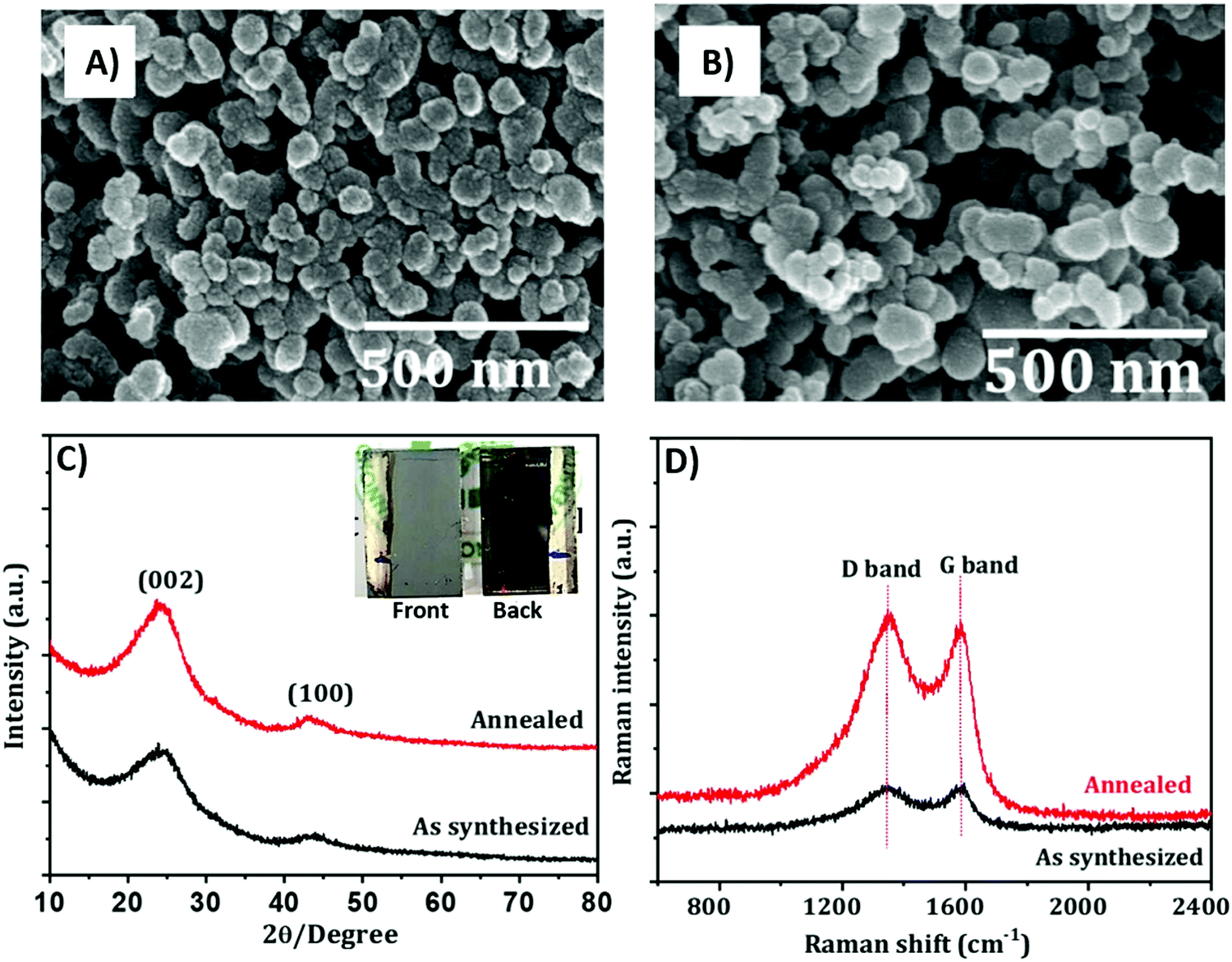 | ||
| Fig. 3 SEM images of the extract from the Aloe Vera plant (A) before and (B) after annealing. (C) XRD and (D) Raman spectra of the extract before and after annealing. The inset in (C) shows optical images of Aloe Vera-derived PSCs from both front and back views. Adapted and reprinted with permission from ref. 93. | ||
High-temperature processed carbon may suffer from poor contact with the perovskite phase in mesoscopic PSCs. In fact, bulk graphite has a large grain size, with small specific surface area. However, to ensure a good contact with the perovskite phase, a material with large surface area and interconnected channels is required. For this reason, malleable ultrathin graphite (UG) was used instead of bulk graphite (BG) for the first time by Duan et al. as a cathode material for PSCs.94 UG was prepared by mechanical exfoliation of BG and mixed with carbon black. The latter is a fine carbonaceous powder, with small particles, that breaks the extremely oriented and impermeable graphite layer, improving infiltration phenomena. As confirmed by SEM images shown in Fig. 4A–D, although particle dimensions of BG and UG were similar, UG had a more malleable morphology, better suited for the perovskite phase, and that ensured an effective pore filling of the precursor solution. In addition, the specific surface area of UG (202.24 m2 g−1) was remarkably higher than that of BG (69.01 m2 g−1). A UG-based cell resulted mostly in higher FF (Voc = 901 mV, Jsc = 22.97 mA cm−2, FF = 0.68, PCE = 14.07%) with respect to that of the BG-based one (Voc = 893 mV, Jsc 22.89 mA cm−2, FF = 0.62, PCE = 12.63%), measured with reverse scan direction.
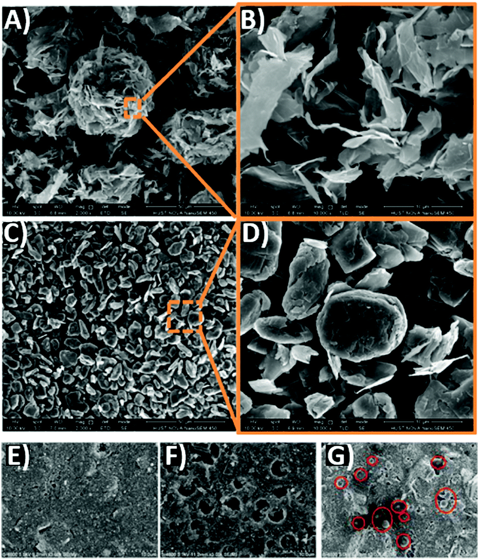 | ||
| Fig. 4 SEM images at low and high magnification of (A and B) UG and (C and D) BG, highlighting that the UG sheets tend to stick together to form a fluffy agglomerate; UG has a diameter of 5–15 μm, similar to BG. SEM images of (E) pristine carbon paste, (F) PSs-10% carbon paste before and (G) after thermal treatment. Adapted and reprinted with permission from ref. 94 and 95. | ||
Another strategy for improving the contact of carbon with perovskites is the use of a volatile, pore forming agent in carbon pastes. When the carbon paste is deposited and thermally treated, this agent decomposes and leaves pores that facilitate the penetration of the perovskite precursor solution into the mesoporous structure. In 2018, Tao et al. used different contents of polystyrene spheres (PSs) as pore forming agents in carbon pastes, in order to obtain a highly porous carbon back electrode for PSCs.95Fig. 4E shows the pristine material, deposited by screen-printing. Fig. 4F shows the PSs–10% carbon paste before annealing, with PSs clearly visible on the surface. After the thermal treatment, PSs were removed, leaving a highly porous material, as shown in Fig. 4G. The weight ratio of PSs with respect to the carbon paste had an effect on the PCE of the resulting devices. In fact, the optimal percentage was 10%, with a Voc of 782 mV, a Jsc of 9.32 mA cm−2, a FF of 0.56 and a PCE of 4.10%; these values were improved with respect to those of the pristine material (Voc = 704 mV, Jsc of 8.36 mA cm−2, FF = 0.55 and PCE = 3.36%). A further increase in the PSs content brought to a reduced PCE of 3.13%, mainly due to the decreased conductivity of the carbon electrode.
One of the main issues with carbon-based PSCs is the high resistance of the cell and the uncontrolled crystallization of the perovskite phase in the porous stack. An attempt to reduce the sheet resistance and ameliorate interfaces between printed stacks was made by Hashmi et al. in 2017.96 They reported a humidity-assisted thermal exposure (HTE) as a post-treatment method for PSCs. After the pore filling of the substrate with the perovskite precursor solution (one-step deposition method), the cell was exposed to 70% relative humidity (RH) for 115 h. This treatment resulted in a drastic enhancement of the preliminarily measured PV parameters. Also, the hysteresis effect was reduced. This beneficial effect may be ascribed to two main factors: first of all, the sheet resistance of the carbon layer, measured by the four-probe sheet resistance method, was found to drastically reduce after the HTE treatment. Water molecules probably increased the interconnectivity between carbon nanoparticles (NPs) and perovskite crystals. Secondly, the hydrophobic carbon impeded the fast intrusion of water drops, that would have led to the decomposition of the perovskite, and allowed only the penetration of gaseous water molecules. Perovskite growth under humidity was already demonstrated by You et al.97 Larger crystals, with an optimal contact with both anode and carbon layer, were obtained. One batch of devices was stored at 40 °C under full sun illumination and retained 92% of its initial efficiency after 350 h, confirming the irreplaceable role of hygroscopic carbon in preventing moisture penetration.
A suitable strategy to further enhance PSC efficiency is the replacement of a methylammonium (MA) cation98 with 5-amino valeric acid (5-AVA)99 or formamidinium (HC(NH2)2+, FA).100,101 When 5-AVA is added in the precursor solution, it replaces the MA cation in the cuboctahedral site of MAPbI3. 5-AVA templates the crystallization of the perovskite in the pores of mesoporous TiO2, providing a lower defect concentration,99 while its –COOH and –NH2 groups interact with TiO2 through hydrogen bonding, ensuring a better interfacial contact with the anode.102 Mei reported an increase in PCE from 7.2% to 11.6% by replacing MA with 5-AVA,99 while Santhosh reported an average PCE of 6.47% for the same cell (see Table 2).102 The lower PCE was ascribed to the poor FF, due to a non-optimal assembly of the cell. On the other hand, the FA cation forms a perovskite phase with a band-gap of 1.47 eV, lower than that of MAPbI3 (1.55 eV). FAPbI3 has a stronger absorption in the visible range with respect to MAPbI3, so it can convert light into electricity more efficiently. In 2014, Hu et al. for the first time incorporated FAPbI3 into a carbon-based PSC.100 The band alignment of FAPbI3 with respect to the TiO2 anode and carbon electrode was favorable for electron and hole injection, respectively, as shown in Fig. 5A. As a matter of fact, the Jsc slightly increased, passing from 17.5 to 18.4 mA cm−2. On the other hand, the Voc decreased, so the PCE was rather unchanged (see Fig. 5B). The mixed perovskite, with both cations, permitted attainment of higher Jsc and PCE values, as reported in Table 2.
| Perovskite | V oc (mV) | J sc (mA cm−2) | FF | PCE (%) | Ref. |
|---|---|---|---|---|---|
| MAPbI3 | 855 | 13.9 | 0.61 | 7.2 | 99 |
| (5-AVA)x(MA)1−xPbI3 | 843 | 21.1 | 0.65 | 11.6 | 99 |
| (5-AVA)x(MA)1−xPbI3 | 858 | 22.8 | 0.66 | 12.84 | 99 |
| (5-AVA)x(MA)1−xPbI3 | 830 | 15.6 | 0.49 | 6.47 | 102 |
| MAPbI3 | 928 | 17.5 | 0.70 | 11.4 | 100 |
| FAPbI3 | 901 | 18.4 | 0.72 | 11.9 | 100 |
| (FA)0.6(MA)0.4PbI3 | 921 | 20.9 | 0.67 | 12.9 | 100 |
| MAPbI3 | 900 | 11.41 | 0.60 | 6.30 | 103 |
| PEA-MAPbI3 | 900 | 16.12 | 0.60 | 8.68 | 103 |
| CsPbBr3 (mesoscopic) | 1270 | 6.29 | 0.60 | 4.77 | 125 |
| CsPbBr3 (planar) | 1330 | 5.09 | 0.55 | 3.67 | 125 |
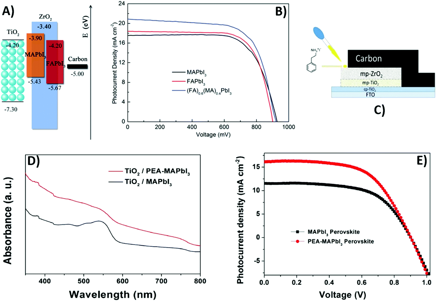 | ||
| Fig. 5 (A) Band alignment of MAPbI3 and FAPbI3 perovskites with respect to TiO2 and carbon. (B) J–V curves of MAPbI3-based (black), FAPbI3-based (red) and (FA)0.6(MA)0.4PbI3-based (blue) cells. (C) Device configuration of fully printable MAPbI3- and PEA-MAPbI3-based PSCs, and a comparison of their (D) absorption spectra and (E) J–V curves. Adapted and reprinted with permission from ref. 100 and 103. | ||
A similar strategy was followed by Xu et al. in 2018.103 Phenethylammonium iodide (PEAI) was introduced into the perovskite precursor solution as an additive, as shown in Fig. 5C. Similar to 5-AVA, the phenethylammonium (PEA) cation improved the contact with TiO2 at the interphase, ensured a better pore filling of the solution and lowered the defect concentration in the perovskite film. As a matter of fact, the crystallinity of the perovskite material increased and the film was adherent to the mesoporous TiO2. As demonstrated by time-resolved photoluminescence (PL) spectra,104,105 the exciton lifetime in PEA-MAPbI3 was much longer (40 ns) with respect to that in MAPbI3 (12 ns). PEA-MAPbI3 also exhibited a stronger absorption than MAPbI3 in the range 350–800 nm, as shown in Fig. 5D. These optimized properties resulted in a higher Jsc (from 11.41 to 16.12 mA cm−2, see Table 2 and Fig. 5E), thus leading to a higher overall PCE.
The main problem associated with MA- and FA-based perovskites is the poor stability under air moisture and heat.106–110 For these reasons they require a strong humidity control (e.g., glovebox conditions) during the fabrication process and are not suitable for real outdoor conditions, where high temperatures can be easily reached.111–113 In order to increase their stability, the organic moiety may be partially or totally eliminated.114–116 Caesium(I) is a suitable large cation that can be easily incorporated into lead-based perovskites, both in mixed-cation perovskites117,118 and in fully inorganic CsPbI3 perovskites.119,120 Despite a remarkable initial PCE of 10%,121 inorganic CsPbI3 underwent an irreversible transformation toward a non-perovskite phase. Therefore, the stability was seriously compromised.121,122 However, the thermal stability can be increased by fully replacing iodide with bromide.123,124 In fact, CsPbBr3 is stable till 580 °C125 and presents great charge transport ability and mean free path.126 This perovskite was used in planar PSCs and showed a remarkable stability for more than three months in humid air.122 For the first time, in 2018 Poli et al. demonstrated that CsPbBr3 was able to work as an active material also in mesoscopic PSCs.125 The mesoporous carbon layer was annealed at different temperatures, ranging from 100 to 400 °C. Samples annealed below 400 °C still presented traces of organic binder present in carbon pastes. Only for the sample annealed at 400 °C a pure perovskite phase was found. The PV parameter that was mostly influenced by temperature was the Voc. In fact, the presence of other species can truly influence the recombination rate.127,128 The optimal annealing temperature was 400 °C, and the corresponding devices showed an average Voc of 1.27 V, a Jsc of 6.29 mA cm−2, a FF of 73.5 and a PCE of 4.77% (see Table 2). For comparison, an analogous planar architecture was also reported, which presented a lower PCE (3.67%), even if the Voc was higher (1.33 V) as shown in Table 2. This was ascribed to the fact that high-temperature treated mesoporous carbon presented high roughness, which allowed the permeation of the precursor solution and ensured a more effective contact with the perovskite phase, with respect to the planar carbon layer.
TiO2 is the most used anodic material not only for PSCs, but also for dye-sensitized solar cells (DSSCs).129–141 It presents several advantages, such as low cost, low toxicity, adequate band-gap and high electron collection efficiency. Some efforts have been made to further ameliorate its performance in carbon-based PSCs. In 2014, Rong et al. synthesized TiO2 nanosheets (NSs) by a hydrothermal route in hydrofuran solution, and compared the resulting PCE with that of TiO2 NPs.142 The structure of TiO2 NSs ensured a higher number of (001) facets, with respect to that observed for TiO2 NPs, due to the elongated geometry. It was found that the (001) anatase facet was slightly more reactive than the (101) counterpart because of the larger number of titanium atoms without coordination.143 In addition, the (001) facet presented a higher charge density, that may strengthen the interaction with the active absorbing material. Consequently, electron injection was facilitated.144,145 As shown in J–V curves (see Fig. 6A), Voc, Jsc and PCE of the NSs-based device were higher than those of the NPs-based one (868 mV, 20.1 mA cm−2 and 10.64% vs. 839 mV, 13.7 mA cm−2 and 7.36%); a TEM image of NSs is shown in Fig. 6B.
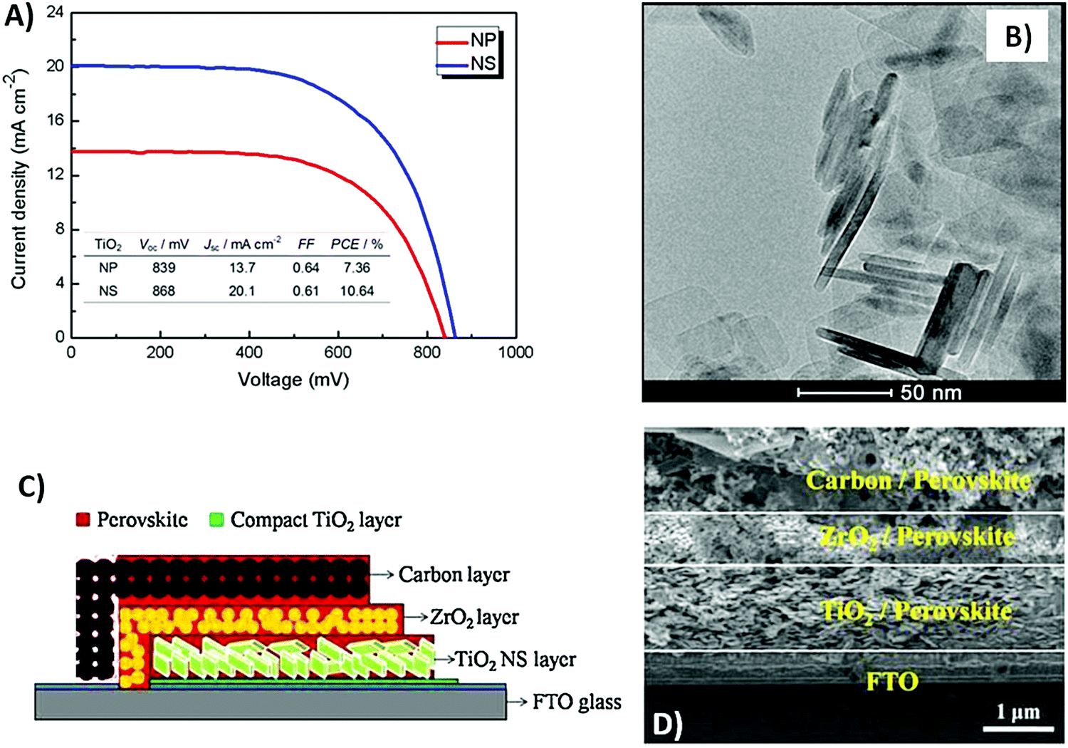 | ||
| Fig. 6 (A) J–V curves of NPs- and NSs-based PSCs under AM 1.5 simulated sunlight of 100 mW cm−2 and, in the inset, the corresponding PV parameters; (B) TEM images of TiO2 NSs. (C) Schematic structure of a PSC with a 4-layer structure, bearing the perovskite infiltrated through the carbon electrode; (D) cross-sectional field emission SEM (FESEM) image of a PSC where a TiO2 NS layer and the carbon electrode are separated by a ZrO2 layer to avoid direct contact. Adapted and reprinted with permission from ref. 142 and 146. | ||
Similar results were obtained by Zhang et al. in 2018.146 They built two types of 1 μm-thick anodes, one based on TiO2 NSs (see Fig. 6D) and the other one based on TiO2 NPs. The PCE of the NS-based device shown in Fig. 6C was almost twice that of the NP-based one (8.11% vs. 4.37%, respectively), confirming that the (001) anatase facet was more reactive and suitable for perovskite adhesion and electron injection. In addition, they varied the TiO2 layer thickness from 0.3 to 1.4 μm, and found that the best results were provided by 1 μm-thick TiO2. In fact, recombination decreased by increasing the layer thickness, as confirmed by electrochemical impedance spectroscopy (EIS) analysis.147 However, a too thick TiO2 layer caused high series resistance.
Another strategy used to ameliorate the anode performances is the surface modification of TiO2. In 2015, Liu et al. reported a HTM-free PSC with an organic silane self-assembled between TiO2 and the perovskite.148 The silanization of the anode was achieved by dipping a high-temperature processed TiO2/ZrO2/carbon substrate and subsequent hydrolysis. This extra layer drastically reduced recombination processes at the interphase between the perovskite and TiO2, as confirmed by the drastically increased recombination resistance in the EIS spectrum. PCE values were determined as a function of silane treatment time. Efficiencies of 9.71%, 11.10%, 12.41%, 12.77% and 10.44% were reached with treatment times of 0, 0.5, 1, 4 and 24 h, respectively. Therefore, the PCE increased with treatment time, till a maximum of 4 h. After that, an excess of silane on the TiO2 surface caused poor infiltration of the perovskite precursor solution.
In order to replace expensive HTMs, many p-type inorganic semiconductors have been reported. Among them, NiO showed several advantages, such as low cost, stability, wide band-gap and high hole mobility.149 In 2015, Cao et al. used NiO as the HTM and reported a TiO2/Al2O3/NiO/carbon architecture with infiltrated perovskite precursor solution, as shown in Fig. 7A.150 All layers were deposited by the screen-printing method, ensuring a reproducible and scalable procedure. NiO successfully increased the PV efficiency. As a matter of fact, the PCE increased from 11.20% (for the NiO-free PSC) to 15.03% (for the NiO-containing PSC). It was suggested that NiO limited charge recombination and ameliorated hole collection efficiency toward the carbon electrode.
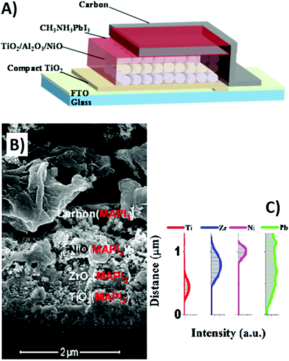 | ||
| Fig. 7 (A) A carbon-based PSC architecture composed of four printed layers. (B) Cross-sectional SEM of TiO2/ZrO2/NiO/carbon(MAPbI3) and (C) atomic distribution obtained by energy dispersive X-ray (EDX) analysis. Adapted and reprinted with permission from ref. 150 and 151. | ||
A similar architecture was reported in the same year by Xu et al.151 ZrO2 was used as both spacer and insulator to keep the TiO2 anode and NiO semiconductor separated. The resulting TiO2/ZrO2/NiO/carbon(MAPbI3) architecture presented a p–i–n configuration as shown in Fig. 7B and C. Besides enhancing charge collection at the interface with the carbon back electrode, NiO successfully acted also as an electron blocking layer, thus reducing charge recombination. As a matter of fact, the device with this architecture attained remarkably high photovoltaic performances, with a Voc of 917 mV, a Jsc of 21.36 mA cm−2, a FF of 0.76, an average PCE of 13.7% and a maximum PCE of 14.9%. Long-term stability of the device was confirmed, since at room temperature and at 40% RH it retained 93% of the initial PCE after 1000 h of aging under dark conditions. The device was not sealed; in fact, hydrophobic carbon can prevent atmospheric moisture from penetrating the perovskite layer.
Charge transport in NiO can be attributed to positively-charged nickel vacancies. By increasing the temperature, the removal of some nickel(II) cations results in increasing the number of oxygen atoms surrounding the remaining nickel atoms. For this reason, some nickel(II) are oxidized to nickel(III) and conductivity is attributed to hole hopping from the Ni3+ sites to Ni2+ ones. To further enhance charge mobility, NiO can be treated with ultraviolet (UV)/O3 and annealed at high temperature. The UV/O3 treatment generates NiOOH species on the surface of nickel oxide. Hydroxyl groups are then removed by thermal treatment. Ni2O3 with a low transport resistance and a high charge mobility is formed. This treatment has been used by Behrouznejad et al. to provide a mesoscopic PSC with a NiO/carbon back electrode.152 When a 450 nm-thick Al2O3 space layer was used, an average PCE of 11.28% (with best device having a PCE of 12.12%) was achieved. However, a drop in PCE of 18.2% was observed after three months.
Aside from NiO, other transition metal oxides were taken into account as the HTM for PSCs.153 However, it was found out that only NiO had a positive effect on PV parameters. In fact, MoO3, Co2O3 and CuO did not ensure an efficient interaction with the perovskite phase and the PCEs of the corresponding devices were quite lower than those of NiO-based devices: 0.82%, 6.93%, 6.08% and 13.94%, respectively.
Besides using NiO as the HTM, heteroatomic doping of graphite may be a suitable strategy for modifying the work function of carbon electrode and facilitating charge extraction.154,155 In fact, the tiny difference between the work function of carbon and the valence band of perovskite causes a carrier extraction barrier at the interphase, limiting PV performances. Carbon atoms in the graphitic layers can be easily replaced by electron-deficient boron by high-temperature thermal treatment with B4C, as shown in Fig. 8A.156,157 After this treatment, the work function of the carbon electrode was improved by the incorporation of the electron-deficient boron atom (5.10 vs. 4.81 eV of pure graphite, PG). In addition, boron-doped graphite (BdG) showed a lower sheet resistance (16 vs. 35 Ω sq−1 of the PG). This was attributed to a better graphite layer packing and higher graphitization degree, as confirmed by XRD patterns. BdG-based devices showed improved Voc, FF and PCE with respect to PG-based cells (940 mV, 0.63 and 13.6% vs. 900 mV, 0.60 and 12.4%, respectively). The increased FF and reduced hysteresis effect were ascribed to the more favorable band alignment in BdG-cells.157
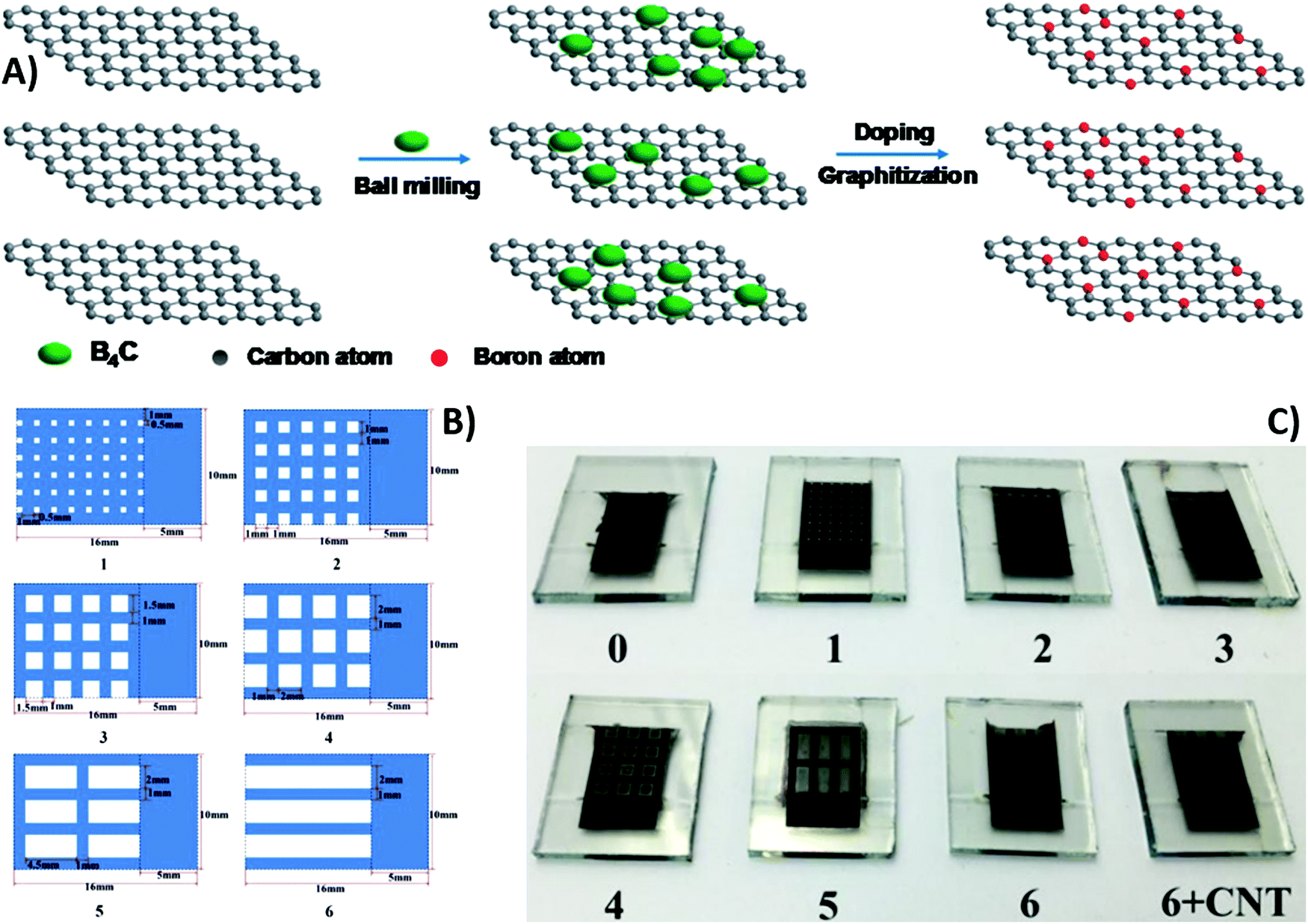 | ||
| Fig. 8 (A) Preparation of BdG starting from graphite and B4C. (B) Schematic diagrams of carbon back electrodes with different carbon grids (blue represents carbon), and (C) optical images of as-fabricated semitransparent PSCs. Adapted and reprinted with permission from ref. 157 and 162. | ||
Other alternatives to NiO are p-type spinel oxides that are promising HTMs due to their excellent hole mobility. The first use of p-type Co3O4 as the HTM in carbon-based PSCs was reported in 2018 by Bashir et al.158 Co3O4 has a cubic structure with high spin Co(II) in the tetrahedral sites and low spin Co(III) in the octahedral sites. In addition, the Co3O4 VB (−5.3 eV) matches well with that of perovskite (−5.4 eV), favoring efficient hole extraction. The effective contact between the perovskite and cobalt oxide and the improved hole extraction at the carbon electrode were demonstrated by the negligible hysteresis effect and by a high PCE of 13.27% (Voc = 0.88 V, Jsc = 23.43 mA cm−2, FF = 0.64).
Despite their dark appearance, carbon-based materials can also be used as transparent electrodes, necessary for semitransparent solar cells.159 An ideal transparent electrode should exhibit high transparency, low resistance and charge collection efficiency. In this view, a thick layer of carbon-based materials may be the ideal candidate. Graphene and CNTs have already been successfully applied as back electrodes in semitransparent PSCs.160,161 However, in most cases, they are still prepared by non-scalable procedures, such as transferring and lamination. For these reasons, in 2017 Li et al. reported for the first time a fully printable carbon-based PSC with a TiO2/(5-AVA)0.05(MA)0.95PbI3/Al2O3/carbon architecture.162 The carbon layer was deposited by the screen-printing method, using several grids with different geometries, as reported in Fig. 8B and C. For comparison, a carbon-based PSC without grid lines was also fabricated (device 0). Device 1 showed the best performances, even when compared to device 0, with a Voc of 0.87 V, a Jsc of 21.07 mA cm−2, a FF of 58.9% and a PCE of 10.80% (Table 3). This result was due to the fact that the smaller grid lines of device 1 ensured a better pore filling of the perovskite precursor solution. The decreased PCE with increasing number of grid lines was ascribed to the increase in series resistance of the electrode. To solve this issue, MWCNTs were coated on top of device 6. MWCNTs enhanced conductivity by creating a charge transport network. In fact, the PCE dramatically increased from 5.08% to 8.04%.
| Device | V oc (V) | J sc (mA cm−2) | FF (%) | PCE (%) |
|---|---|---|---|---|
| 0 | 0.85 | 20.16 | 52.5 | 9.00 |
| 1 | 0.87 | 21.07 | 58.9 | 10.80 |
| 2 | 0.85 | 20.21 | 53.6 | 9.21 |
| 3 | 0.85 | 18.87 | 53.8 | 8.63 |
| 4 | 0.85 | 16.66 | 56.3 | 7.97 |
| 5 | 0.84 | 13.97 | 51.3 | 6.02 |
| 6 | 0.84 | 11.32 | 53.4 | 5.08 |
| 6 + MWCNTs | 0.87 | 17.94 | 51.5 | 8.04 |
Further issues for the realization of scalable high-temperature processed carbon-based PSCs are (i) mechanical infiltration of the perovskite solution, in order to have a fully reproducible and printable fabrication method;163 (ii) long-term stability under UV-light soaking;164,165 (iii) high-temperature thermal stability;166 and (iv) enlargement of the active area of the cell.167 The manual infiltration of the perovskite precursor solution onto the carbon layer limits reproducibility and is also time-consuming. For this reason, Hashmi et al. reported in 2017 a suitable strategy for the inkjet infiltration of the perovskite ink in HTM-free carbon-based PSCs.163 The precursor ink was loaded into a disposable cartridge and deposited by an inkjet printer on the high-temperature processed carbon electrode. 5-AVA iodide was added in the precursor ink to slow down perovskite crystal growth, thus preventing the inkjet printer cartridge from clogging and ensuring a better filling through the carbon layer. In particular, 10 × 10 cm2 fluorine-doped tin oxide (FTO)-glass substrates having 18 individual cells of HTM-free triple layer PSCs were fabricated, as shown in Fig. 9A. Photovoltaic parameters showed improved reproducibility, with average values of 0.845 V (Voc), 15.2 mA cm−2 (Jsc), 0.635 (FF) and 8.15% (PCE). PCE of the devices stored under dark conditions was found to initially increase by 13% in the first three weeks. This was ascribed to a further curing of the perovskite phase. Then, the PCE restored to its initial value and remained stable for 1046 h. On the other hand, the stability under sunlight soaking conditions at 35 °C was also determined. In this case, after 1046 h, the drop in PCE was only 4.5%. The sluggish degradation of the perovskite, with formation of PbI2, was observed and monitored by the camera imaging technique.
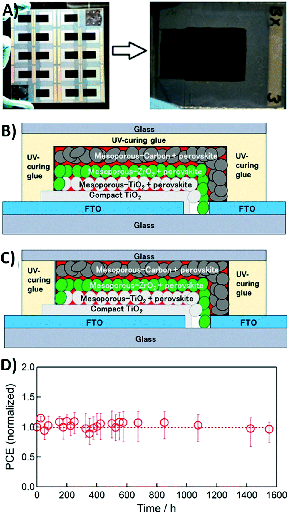 | ||
| Fig. 9 (A) A 10 × 10 cm2 FTO-glass from which 18 PSCs were fabricated with a scalable and printable process; the resulting PSC after the mechanical infiltration of the precursor ink is shown in the right side. Architecture of (B) the over-sealed and (C) the side-sealed carbon-based PSCs. (D) Variation of the average normalized PCE of three replicates of over-sealed PSCs during thermal stability testing at 100°C in the dark; each data point represents an average between the forward and reverse scans. Adapted and reprinted with permission from ref. 163 and 166. | ||
UV light exposure has been identified as one of the key issues for the evaluation of PSCs’ long-term stability.168–171 For this reason, the same cells obtained by inkjet printing and stored without encapsulation were subjected to intense 1.5 sun UV light illumination in an electronic weather chamber, at 45% RH and 40 °C.164 In the first 250 h, the cell ameliorated its performances in both Jsc (+17%) and PCE (8.6%); this behavior may be ascribed to the additional curing of perovskite crystals under UV light. After this time, a slow degradation of cell performance started. Part of the dark-brown perovskite layer became yellow after 751 h, due to the formation of PbI2 and the disappearance of HI and CH3NH2. The Jsc reduced by 25% and the PCE by 28%. Some batches were sealed with epoxy glue to prevent contact with moisture. Epoxy did not dissolve any phase and did not penetrate into the carbon layer over the photo-active area. In these cells, the average Jsc and PCE were maintained after 1002 h. XRD demonstrated that PbI2 reflections appeared only in epoxy-free aged samples. PL measurements demonstrated that the carrier lifetimes of batch 1 (without epoxy) and batch 2 (with epoxy) were 21.6 ns and 4.1 ns, respectively. This means that the epoxied samples were more likely to accelerate light-induced charge separation, thus restricting charge recombination, which correlated well with the results of aging tests.
Thermal stability is necessary for outdoor application of PSCs in many warm areas of the Earth, for example desert regions. However, the perovskite undergoes a phase transition from tetragonal to cubic at 54 °C.172 For these reasons, Baranwal et al. reported a three-layer printable HTM-free PSC with carbon as the back electrode, able to keep stability till 100 °C.166 Despite the hydrophobic nature of this carbon component, owing to its porous nature, sealing of the device was necessary under high-temperature conditions. Sealing was conducted with a UV-cured gel and a glass cover, in two different configurations (over-sealed and side-sealed, as shown in Fig. 9B and C). Sealed and unsealed devices were kept at 100 °C before measuring J–V curves. Both the unsealed and over-sealed devices lost 20% of their initial efficiency in the first 30 h. In contrast, side-sealed devices did not degrade during thermal tests and their PCE remained constant over 1500 h (see Fig. 9D), suggesting that sealing is a necessary protection against moisture, but it could also cause internal decomposition in the over-sealed configuration.
Finally, the enlargement of the active area of the cell is a desirable goal for the real application of a PV solar cell. However, this task is not trivial when a thermal treatment, which may cause the cracking or the bending of the glass, is involved. Both high-temperature treated TiO2 and carbon may suffer from poor uniformity and compactness. In 2018, De Rossi et al. reported the first example of A4-size carbon-based PSC, with an active area of 198 cm2.167 They optimized the printing process with the method of edge registration to avoid short circuit and damage to the layers. The PSC was composed of 22 units, with dimensions of 5 × 180 mm2 and spaced by 6 mm, as shown in Fig. 10. A 1.5 mm-wide ZrO2 layer and a low-temperature-treated TiO2 layer were used as the insulator and blocking layer, respectively. A 10 μm-thick carbon layer was deposited by the doctor-blade technique in order to minimize the series resistance between adjacent units. With this large-area device, the highest PCE was 3.2%.
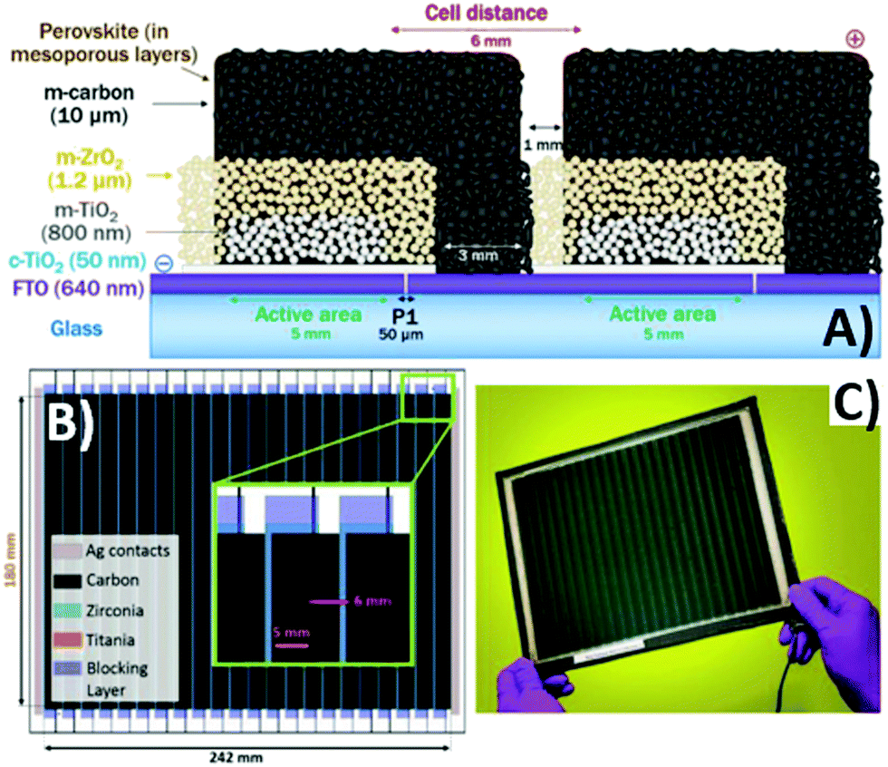 | ||
| Fig. 10 (A) Cross-section schematics of adjacent cells in the module with nominal thickness of each layer, highlighting the laser-etched FTO, patterning of TiO2 blocking layer and the electrical vertical connection, ensured by the carbon back contact; (B) module schematics, showing the different overlapping layers, the dimensions of the active area for both the individual single cell and the whole module as well as the distance between adjacent cells (inset); (C) photo of a module; wires have been soldered to the silver painted busbars to provide more robust electrical contacts. Adapted and reprinted with permission from ref. 167. | ||
2.2 Low-temperature processed back electrodes
High-temperature thermal treatment of carbon-based electrodes is a time and energy-consuming method, that may limit large-scale manufacturing of PSCs.173 In addition, high-temperature processed carbon cannot be applied in plastic and flexible devices. In 2014, Wei,174 Zhou175 and Zhang22 reported the first examples of low-temperature processed carbon electrodes for PSCs. In particular, the innovation introduced by Wei was the use of an ink containing both carbon and CH3NH3I in isopropanol, that was directly printed on FTO/TiO2/PbI2, as shown in Fig. 11A.174 In this way, the deposition of the carbon layer and the formation of perovskite phase occurred simultaneously, ensuring an efficient interfacial contact between CH3NH3PbI3 and carbon. For comparison, another cell was prepared by the “traditional” route: after the deposition of the carbon layer onto the FTO/TiO2/PbI2 substrate, the cell was soaked into the CH3NH3I solution. The intimate contact between the two phases was better in the first case, when carbon was deposited together with the CH3NH3I solution, as confirmed in the SEM images shown in Fig. 11B and C. Recombination resistance (Rrec) was estimated by fitting EIS data. It was confirmed that charge recombination was several times lower in the cell obtained with the CH3NH3I/carbon ink. Consequently, PV parameters improved: Voc increased from 0.90 to 0.95 V, Jsc from 15.00 to 17.20 mA cm−2, FF from 0.63 to 0.71 and PCE from 8.51 to 11.60%. Finally, devices maintained about 90% of their initial PCE after 12 days of dark storage without sealing.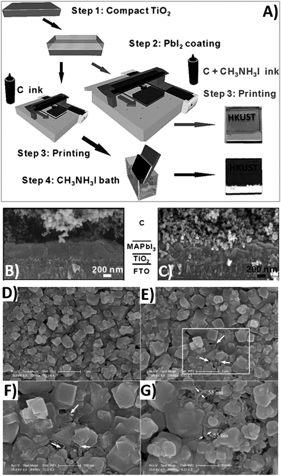 | ||
| Fig. 11 (A) Fabrication process flow for the instant inkjet printing of the carbon/CH3NH3PbI3 planar PSCs; cross-sectional SEM images of TiO2/CH3NH3PbI3/carbon solar cells prepared by the inkjet printing technique using (B) a carbon ink and (C) a carbon + CH3NH3I ink (the increased interconnectivity between the perovskite and carbon phase can be clearly seen in the right image). (D) Planar SEM images of a pristine perovskite film and of (E–G) films obtained with addition of 0.1 mg mL−1 MWCNTs: the contact between perovskite grains was increased after the addition of MWCNTs. Adapted and reprinted with permission from ref. 174 and 179. | ||
Zhou et al. investigated for the first time the influence of carbon layer thickness on the performance of low-temperature processed PSCs.175 Carbon particles were dispersed in chlorobenzene and deposited by the doctor-blade technique, varying the thickness in the range 2–40 μm. It was found that the PCE of devices increased with carbon layer thickness till a maximum of 20 μm. 2.1 μm-thick carbon presented a high sheet resistance of 160 Ω, therefore the corresponding cell exhibited a poor PCE of 2.25%. On the other hand, the best PCE of 6.90% was obtained with a carbon layer thickness of 20.6 μm. Even though a clear explanation for this structure–performance correlation was not provided by the authors, cell stability was confirmed for up to 2446 h. Such a good result under long-term testing was ascribed to the presence of hydrophobic carbon, which impeded the penetration of moisture, and to the absence of noble metals, which could corrode CH3NH3PbI3.
The intrinsic resistivity of graphite is high. However, it can be reduced by introducing carbon black NPs (CBNPs)176 and nano-graphite powder177 or by ameliorating carbon morphology.178 Within the carbon electrode, charge transportation is provided mainly by graphite flakes; the addition of CBNPs facilitates the connections between them and improves the interfacial contact with the perovskite phase.176 In literature studies, PV parameters were influenced by the relative content of CBNPs with respect to graphite. In fact, the addition of CBNPs in the ratios 5:1 and 3:1 dramatically increased the PCE, as shown in Table 4 (entries I–III). This improvement was attributed to the reduced sheet resistance of the carbon material, that changed from 1.11 to 0.69 Ω cm (after having been pressed at 0.25 MPa). However, a further increase of CBNPs (ratio 2:1) slightly diminished cell performances (see Table 4, entry IV); in fact, an excess of CBNPs brought about a stronger recombination.176
| Entry | Carbon electrode composition | V oc (V) | J sc (mA cm−2) | FF | PCE (%) | Ref. |
|---|---|---|---|---|---|---|
| a Indicates cells fabricated under high humidity conditions. | ||||||
| I | Graphite | 0.97 | 18.8 | 0.57 | 10.27 | 176 |
| II | Graphite/CBNPs 5:1 |
0.98 | 20.0 | 0.58 | 11.43 | 176 |
| III | Graphite/CBNPs 3:1 |
1.00 | 21.3 | 0.63 | 13.53 | 176 |
| IV | Graphite/CBNPs 2:1 |
0.97 | 20.6 | 0.62 | 12.47 | 176 |
| Va | Graphite/CBNPs 3:1 |
0.79 | 13.0 | 0.43 | 4.47 | 177 |
| VIa | Graphite/CBNPs/nanographite powder (400 nm) 1:1:2 |
0.82 | 14.9 | 0.43 | 5.31 | 177 |
| VIIa | Graphite/CBNPs/nanographite powder (40 nm) 1:1:2 |
0.84 | 16.8 | 0.43 | 6.16 | 177 |
| VIIIa | Graphite/CBNPs/nanographite powder (40 nm) 1:1:5 |
0.87 | 11.0 | 0.40 | 3.84 | 177 |
| IX | Self-adhesive carbon film | 1.08 | 23.3 | 0.76 | 19.2 | 178 |
| X | Carbon | 0.87 | 20.2 | 0.56 | 9.8 | 179 |
| XI | Carbon/MWCNT | 0.93 | 21.3 | 0.59 | 11.6 | 179 |
A similar strategy was followed by Liu and coworkers.177 Besides CBNPs, they also explored the effect of nano-graphite powder with different particle dimensions of 40 and 400 nm. The introduction of nano-graphite powder made the carbon film more compact and improved the interfacial contact. Thus, PV performances ameliorated after the introduction of nano-graphite powder. Table 4 (entries VI and VII) reveals that cells containing smaller nano-graphite powder (40 nm) perform better than cells containing larger graphite powder (400 nm). Larger particles decreased the contact between grains, establishing an overpotential at the interphase. However, increasing the content of 40 nm-graphite powder did not lead to a further increase of PCE (see Table 4, entry VIII). In fact, too much nano-graphite powder could have led to higher resistance and stronger recombination.
It has to be noted that, even though the cell architectures are identical, PCE values obtained by Wei176 are remarkably higher than those obtained by Liu177 (13.53% vs. 4.47%, respectively), as shown in Table 4 (entries III and V). In fact, the latter researcher fabricated the devices under uncontrolled high humidity conditions, which may have deteriorated the perovskite layer, thus limiting the PCE.
The poor interface contact between carbon and the perovskite phase is the main efficiency-limiting factor of low-temperature carbon-based PSCs with respect to gold-based PSCs. In fact, commercial carbon pastes contain solvents that, during evaporation, can create bulges and pinholes in the material, and also the perovskite layer may present holes that are not filled with the carbon material. A suitable solution to overcome this issue was proposed by Zhang et al. in 2018.178 They fabricated a self-adhesive carbon film, processed at room temperature by the solvent exchange method. A carbon electrode, namely C2, was doctor-bladed on a glass, soaked in ethanol and dried. It exhibited a macroporous, flexible morphology, with a thickness of 60 μm. It was removed from the glass and pressed onto the perovskite layer. The adhesion was ensured by its compressibility: in fact, the thickness was reduced to 31.9 μm, allowing an optimal contact at the interphase. Furthermore, after being pressed, its sheet resistance decreased from 424 to 58 Ω sq−1. For comparison, a carbon electrode, namely, C1, with a similar thickness was created by the traditional route at 100 °C, without being soaked in ethanol and transferred from another substrate. As expected, the PCE of the C2-cell was dramatically higher than that reached by the C1-based cell (19.2% vs. 15.2%, see Table 4, entry IX).
Another suitable solution to overcome the poor contact between the perovskite phase and carbon back electrode was proposed by Cheng et al. in 2016.179 As demonstrated by the SEM image shown in Fig. 11D, the CH3NH3PbI3 layer had a rough surface, with particles of different dimensions. On the other hand, the carbon material was composed of nano-sized carbon black and micro-sized graphite flakes. The latter, due to the large dimension, did not provide an effective contact with perovskite crystals, thus reducing the PCE to 9.8% (see Table 4, entry X). To solve this issue, MWCNTs were used. CNTs consist of a graphene layer bent and joined in one direction, to form a hollow cylinder. MWCNTs are composed of more nested CNTs, aligned together. Similar to other graphene-based materials, CNTs exhibit high electrical conductivity and thermal stability.180 MWCNTs with a diameter of 55 nm were added in the perovskite phase in order to fill the gap between larger and smaller particles, thus creating the interconnect network shown in Fig. 11E–G, where photogenerated charges can easily be transferred. In the MWCNT-based devices, an average PCE of 11.6% was achieved (see Table 4, entry XI).
Zhang22 and Liu181 studied the effect of the nature of the TiO2 anode in low-temperature carbon PSCs. In particular, Zhang22 focused on the effect of TiO2 thickness that ranged from 190 to 830 nm by varying the precursor concentration. A too thin TiO2 film (190 nm) cannot support enough quantity of perovskite, making the electron extraction ineffective. This cell provided a low PCE of 2% and a very low Voc of 0.70 V. On the other hand, a too thick TiO2 film increased the probability of electron recombination. The optimal thickness was 630 nm, which provided the best performing devices, with a Voc of 0.82 V, a Jsc of 16.10 mA cm−2, FF of 52.60 and PCE of 7.40%.
The aim of Liu's work was instead the study of the effect of the TiO2 blocking layer between FTO and TiO2 anode.181 An efficient blocking layer favors the extraction of photogenerated electrons and impedes charge recombination and should not present voids or cracks, which may act as recombination centers. However, during the synthesis of TiO2 by the sol–gel process, the widely used precursor Ti(OC4H9)4 undergoes hydrolysis under atmospheric conditions, resulting in a non-uniform morphology of TiO2. For these reasons, different amounts of diethanolamine (DEA), whose basic character hampers the hydrolysis of Ti(OC4H9)4, were added in the precursor solution. SEM images confirmed that the DEA-free TiO2 blocking layer presented many cracks and voids, with a width of ≈400 nm, that can act as recombination centers. On the other hand, DEA-containing films were compact and homogeneous and fully covered the FTO substrate. A remarkable PCE of 11.92% was observed when a Ti(OC4H9)4:DEA = 1:0.75 ratio was used.
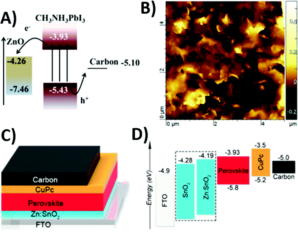
Besides carbon, TiO2 and insulating ZrO2 also require high-temperature sintering and are not suitable for flexible applications, thus hindering the fabrication of PSCs. ZnO is a suitable n-type semiconductor, which requires only low-temperature processing (120 °C) and can be deposited by spin coating.182 Since its conduction band is at a lower energy with respect to that of the perovskite, electron injection is possible between excited CH3NH3PbI3 and ZnO, as shown in Fig. 12A. Therefore, it can replace the role of TiO2. In 2015, Zhou et al. reported the first example of a TiO2- and HTM-free carbon-based PSC with the simple architecture ZnO/CH3NH3PbI3/carbon.182 The thickness of the ZnO layer had a strong influence on PSC efficiency. In fact, a too thin layer (25 nm) was not completely covered by the active material and presented many holes. Its PCE and Voc were limited to 0.90% and 0.47 V, respectively. On the other hand, a too thick ZnO layer (89 nm) showed a high series resistance and an increased recombination rate. In fact, PCE reached a small value of 3.55%, even though its Voc of 0.80 V was the highest found in this kind of system. The optimal ZnO thickness was found to be 55 nm (Voc of 0.74 V, Jsc of 20.68 mA cm−2, FF of 0.46 and PCE of 7.05% in the forward scan).
 | ||
| Fig. 12 (A) Band alignment in ZnO/CH3NH3PbI3/carbon, underlying electron and hole injection from the perovskite and ZnO and carbon, respectively. (B) AFM image of the graphite film on a glass/ITO/ZnO/CH3NH3PbI3 substrate (ITO = indium-doped tin oxide). (C) Schematic cell architecture and (D) energy level diagram for a FTO/Zn:SnO2/perovskite/CuPc/carbon device. Adapted and reprinted with permission from ref. 182, 183 and 186. | ||
Another ZnO-based low-temperature processed PSC was reported by Jin et al. in 2015.183 In this work, all films were deposited at room temperature. An electrochemically exfoliated graphite layer was used as the HTM to improve the extraction efficiency between the perovskite and the carbon back electrode. The obtained graphene had an excellent hole mobility of ≈310 cm2 V−1 s−1. The atomic force microscopy (AFM) image (Fig. 12B) showed that the thickness of graphene sheets was lower than 10 nm, corresponding to 30 atomic layers and the majority of graphite was in the form of NPs. Overall, the carbon-based back electrode was quite compact and completely covered the perovskite film. An average PCE of 7.2% was reached with this architecture.
SnO2 is a high band-gap semiconductor (Eg = 3.6 eV), with high charge mobility and without a UV photocatalytic effect.184 It has already been employed to replace mesoporous TiO2 as the anode material for PSCs, due to its low-temperature processability.185 Metal doping of SnO2 further increases its electronic properties, making it more suitable for application in the PSC field. In particular zinc-doping shifts the work function of SnO2 from −4.28 to −4.19 eV, resulting in a more favorable band alignment, as shown in Fig. 12C. Ye et al. reported in 2019 an entirely low-temperature processed carbon-based PSC with a Zn–SnO2 ETM, as shown in Fig. 12D.186 FF and PCE were strongly improved, with respect to the undoped SnO2-based cell. In particular, PCE increased from 15.31% to 17.78%. The more favorable band alignment generated a stronger electron injection from the excited active material to the ETM.
Even if not necessary, the HTM plays the important role of helping in hole extraction and ameliorating surface contact between the perovskite phase and carbon electrode. The most common organic HTM in gold-based PSCs is spiro-OMeTAD, which is expensive and needs to be doped with LiTFSI to improve conductivity. The latter is a hygroscopic salt that threatens the stability of the perovskite layer.187 Many efforts have been made for the replacement of spiro-OMeTAD with polymeric,188,189 organic24,190,191 and inorganic HTMs.192–194 In this framework, poly(3-hexylthiophene) (P3HT) is an intrinsic semiconductor with high stability (up to 350 °C in air) and low cost. Mashhoun et al. showed in 2018 that it can efficiently work as the HTM in carbon-based PSCs.188 Since the carbon back electrode is usually deposited from carbon pastes, the solvent content in the suspension should not be harmful for the underlying layer. For this reason, the effect of the nature of the solvent was investigated. In particular, the lowest and the highest PCEs were found with chlorobenzene and toluene, respectively (see Table 5, entries I–III). PV performances ameliorated by decreasing the solubility of P3HT in the solvent, but a clear explanation was not given by the authors. Further interface engineering with TaWOx NPs ameliorated the contact between P3HT and carbon, thus enhancing the PCE from 5.04% to 11.58%, as shown in Table 5 (entry IV).
The charge extraction and transport ability of P3HT can be further increased by the addition of graphene. In fact, graphene is a 2D dimensional graphite layer, with high electrical conductivity and thermal stability. In 2019, Chu et al. reported the use of a P3HT/graphene composite as an efficient HTM for carbon-based PSCs.189 The improved properties of the composite were demonstrated by the increase of both PCE and Jsc. PCE shifted from 11.1% to 17.5% and Jsc from 19.3 to 22.3 mA cm−2. FF increased by 45% (from 0.51 to 0.74), suggesting the better contact between the perovskite and the HTM. In their work, a record PCE of 18.2% was reported in the reverse scan.
Small molecule-based HTMs have the advantages of facile synthesis and tunable electronic properties. In addition, in most cases, they do not require the use of a dopant to increase conductivity. Among organic HTMs, copper phtalocyanine (CuPC) is noteworthy.195 It is a strong conjugated planar molecule, with a tendency to form π–π stacking in the film state. Its p-type semiconductor character, low cost, ease of preparation, good thermal stability and long charge diffusion length make it the ideal candidate as the HTM in PSCs.196–198 Zhang et al. used for the first time CuPc as the HTM in carbon-based PSCs.190 Results underlined the importance of CuPc, since every PV parameter improved with respect to the HTM-free cell. In particular, the PCE increased from 9.0 to 16.1%. For comparison, an analogous cell with spiro-OMeTAD as the HTM was also reported. It showed an efficiency of 15.0%, that was still lower than that of the CuPc-cell. In addition, the device with CuPc was more stable: PCE dropped by only 8.5% in 600 h, as shown in Fig. 13A.
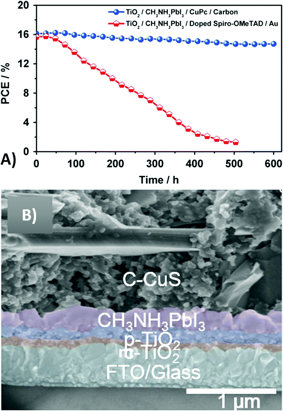 | ||
| Fig. 13 (A) Stability tests of PSCs with CuPc/carbon and doped-spiro-OMeTAD/gold as the HTM and back electrode, respectively. (B) Cross-sectional SEM image of a glass/FTO/c-TiO2/m-TiO2/CH3NH3PbI3/carbon-CuS device, with the following thicknesses; c-TiO2 (70 nm), m-TiO2 (170 nm), perovskite layer (340 nm), carbon electrode (10 μm). Adapted and reprinted with permission from ref. 190 and 192. | ||
Another π-delocalized small molecular HTM was reported by Zhang et al. in 2015.24 Triazatruxene (TAT) contains three indole units combined by one benzene. Due to its electron rich aromatic structure, it has a strong charge carrier ability and has already been employed as the HTM in the field of organic PVs.199,200 Its derivative 5,10,15-triphenyl-5H-diindolo[3,2-a:3′,2′c]carbazole (TPDI) shows the same properties and, in addition, exhibits good thermal stability and compatible band alignment with both carbon and CH3NH3PbI3. When both TPDI and spiro-OMeTAD were doped with LiTFSI, TPDI-based cells showed comparable PCE with respect to spiro-OMeTAD-based ones (15.5% vs. 15.1%, respectively), but without the disadvantages of spiro-OMeTAD. However, the difference was more prominent when the pristine materials were used as the HTM: 13.6% vs. 10.8%, respectively. This inferior performance was ascribed to the relative pure charge transportation ability of spiro-OMeTAD in the absence of a p-dopant and to a larger series resistance. Devices assembled with undoped-TPDI exhibited an increased stability due to its strong hydrophobicity, which prevented the contact between the perovskite and air-moisture. In this kind of cell, the optimal carbon thickness was 10 μm; in fact, 5 μm-thick carbon provided very poor conductivity, while 20–30 μm-thick carbon increased the conductivity, but did not pump PCE. The optimal carbon thickness was different from that reported by Zhou (20 μm), underlining that in the presence of this specific HTM a thinner graphite layer was required.175
In the class of small molecule-based organic HTMs, fluorinated compounds show interesting properties, even though they have not been fully investigated. Due to the small dimension and strong electronegativity of fluorine, fluorination is a suitable strategy for decreasing the energy level, ameliorating hole-extraction at the HTM/perovskite interface.191 A novel fluorinated HTM was reported by Ren et al., i.e. BDT2MeDPA, composed of difluorobenzene, benzo[1,2-b:4,5-b′]dithiophene (BDT) and 4,4′-dimethoxydiphenylamine (DPA) groups.191 Electro-donating BDT presented excellent charge transport properties and facilitated the synthetic process. For comparison, the fluorine-free counterpart (BDT0MeDPA) was also used as the HTM. PV performance remarkably increased with the use of the novel HTM. When BDT0FMeDPA was used, Jsc shifted from 12.5 to 17.2 mA cm−2 and the PCE increased from 8.4% to 11.3%, while Voc maintained a constant value of 0.98 V. BDT2MeDPA-based cells showed a further increase in Jsc (21.4 mA cm−2) and PCE (14.5%), that were slightly lower than those obtained with spiro-OMeTAD (PCE = 15.2%). PL quenching was stronger in the BDT2FMeDPA/perovskite than in the BDT0FMeDPA/perovskite, underlining the well matched energy levels and efficient charge extraction process.
Inorganic p-type HTMs are more thermally stable with respect to molecular ones.201 The most commonly used are CuS,192 CuSCN193 and NiO.194 CuS has already been investigated in DSSCs,202 and was reported as the HTM for PSCs for the first time in 2018. Hu et al. fabricated a carbon-based PSC where small particles of CuS, obtained by a low-temperature precipitation process, were added to the carbon paste to increase the hole-extraction ability of the cathodic hybrid material.192 The resulting carbon electrode had a thickness of 10 μm and CuS presented its nanostructure form below 100 nm, as shown by SEM image in Fig. 13B. The EDX spectrum evidenced the homogeneous distribution of CuS into the carbon electrode.
CuS was added in the carbon paste in the ratio of 0.5–2 wt%. J–V curves evidenced that a small CuS-doping increased by 21% the performances of the carbon-based PSCs. The average PCE shifted from 8.41% for the undoped device to 9.32% for the 0.5%-doped one and 10.22% for the 1%-doped one, highlighting the increased hole collection ability of the doped electrode. On the other hand, efficiency reduced when the amount of CuS exceeded 1 wt%, due to the smaller conductivity of CuS with respect to graphite. For these reasons, the optimal amount of CuS was 1 wt%.
Another copper-based inorganic HTM was reported by Lv et al. in 2018.193 CuSCN is an inorganic p-type semiconductor, with low cost and high stability. It was deposited by spin coating under the perovskite layer with a thickness of 300 nm and established a good contact with both the absorber material and carbon back electrode. It caused a strong emission quenching in the PL spectrum of the perovskite, highlighting its effective contact and suitable band alignment with CH3NH3PbI3. The effect of CuSCN on the PV performance was remarkable: Voc shifted from 0.72 to 0.78 V, Jsc from 17.32 to 19.58 mA cm−2, FF from 0.53 to 0.59 and PCE from 6.61% to 9.01%. This result was confirmed by Mashhoun,188 who found a PCE of 8.59% for CuSCN-based devices.
As already said, NiO has been largely used as the HTM in high-temperature processed carbon-based PSCs.150–152 Its properties of hole conduction and electron blocking effect have been exploited to suppress recombination and increase both Voc and Jsc. However, in high-temperature processed PSCs the poor pore filling causes an inhomogeneous crystallization of the perovskite and this issue is worsened when NiO is used as the HTM. In 2017, Peiris et al. reported for the first time a mesoscopic PSC, with NiO as the HTM and low-temperature processed carbon as the back electrode.194 The perovskite was deposited on the FTO/TiO2/ZrO2/NiO substrate by a modified one-step method in the presence of N2 flow. Subsequently, the carbon film was doctor-bladed on top of NiO: this strategy solved the problem of poor crystallization of CH3NH3PbI3. The PCE was almost doubled up from 5.96% to 10.35% by the presence of NiO. A lower charge transfer resistance was measured by EIS in the NiO-based device, confirming the more effective charge extraction and transfer. In addition, recombination resistance was stronger in NiO-based cells, suggesting that charge recombination was lower.
Another suitable strategy for replacing time and energy-consuming sintering is the NIR technology, that has already been used to thermally treat TiO2 for DSSC application.203 NIR wavelengths are absorbed by a substrate, and converted into heat, causing the rapid warming of the substrate.204 If the substrate is transparent in the NIR range, a metal can be exploited to transfer heat. This method is very fast and allows energy saving. In 2017, Baker et al. reported the use of NIR technology for rapid thermal treatment (12.5 s) in mesoporous carbon-based PSCs.205 Both TiO2 and ZrO2 are transparent in the NIR range, so, when they were deposited and treated with NIR, radiation reached the FTO. The heat generated was enough to burn out all the organic additives of the two pastes. On the other hand, carbon has a high absorption coefficient in the NIR range; so, it absorbed all the radiation that, in this way, did not reach the underlying layer. Heat was generated only in the carbon layer, allowing the evaporation of solvents and volatilization of organic compounds present within the carbon paste. Consequently, the as-formed mesoporous layer was successfully infiltrated with the perovskite precursor solution. To the best of our knowledge, this is the only example of mesoscopic carbon-based PSCs obtained without thermal treatment. The champion device reached a Jsc of 20 mA cm−2 and a stabilized PCE of 11%.
As concluding remarks, a comparison of sheet resistance and thickness of carbon-based back electrodes prepared following different recipes, along with the best PCE values of the resulting devices, is given in Table 6 (for carbon-infiltrated perovskites) and Table 7 (for layered carbon electrodes).
| Paste composition | Deposition technique | Thermal treatment | Sheet resistance (Ω cm−2) | Thickness (μm) | PCE (%) | Ref. |
|---|---|---|---|---|---|---|
| CB/flaky graphite | Blade coating | 400 °C for 30 min | 10.49 | 10 | 4.08 | 29 |
| CB/spheroidal graphite | Blade coating | 400 °C for 30 min | 8.02 | 10 | 6.64 | 29 |
| 2 g CB (particle size 30 nm), 6 g graphite powder, 1 g ZrO2 (particle size 20 nm), 1 g hydroxypropyl cellulose in 30 mL terpineol | Blade coating | 400 °C for 30 min | 11.47 | 9 | 11.63 | 87 |
| 9 g graphite powder (particle dimension <20 μm), 3 g CB, 1 g ZrO2 (particle dimension <100 nm), 15 g ehtylcellulose in 18 g terpineol | Screen-printing | 400 °C for 30 min | 56 | 25 | 10.7 | 88 |
| 5 g graphite, 1 g CB (particle size 30 nm), 1 g ZrO2 (particle size 20 nm), terpineol (30 mL) | Blade coating | 400 °C for 30 min | Not reported | Not reported | 13.7 | 151 |
| BG, CB, hydroxypropyl cellulose, terpineol | Printing | 400 °C for 30 min | 5–20 | 5–16 | 12.63 | 94 |
| UG (obtained by exfoliation of BG), CB, hydroxypropyl cellulose, terpineol | Printing | 400 °C for 30 min | 5–25 | 5–16 | 14.01 | 94 |
| Carbon material (graphite:CB = 3:7), hydroxypropyl cellulose, terpineol |
Screen-printing | 400 °C for 30 min | 23 | 11 | 15.70 | 92 |
| 4 g graphite, 1 g CB, 0.6 g ZrO2, in ethanol | Screen-printing | 400 °C for 60 min | 30.5 | Not reported | 3.36 | 95 |
| 3.8 g graphite, 0.95 g CB, 0.57 g ZrO2, 0.28 g polystyrene spheres in ethanol | Screen-printing | 400 °C for 60 min | 56.7 | Not reported | 3.87 | 95 |
| 3.6 g graphite, 0.9 g CB, 0.54 g ZrO2, 0.56 g polystyrene spheres in ethanol | Screen-printing | 400 °C for 60 min | 68.3 | Not reported | 4.10 | 95 |
| 2.8 g graphite, 0.7 g CB, 0.42 g ZrO2, 1.68 g polystyrene spheres in ethanol | Screen-printing | 400 °C for 60 min | 180.7 | Not reported | 3.13 | 95 |
| 6.5 g graphite, 2 g CB, 1 g ZrO2, 1 g hydroxypropyl cellulose, 30 mL terpineol | Screen-printing | 400 °C for 30 min | 35 | 11 | 12.4 | 157 |
| 6.5 g BdG, 2 g CB, 1 g ZrO2, 1 g hydroxypropyl cellulose, 30 mL terpineol | Screen-printing | 400 °C for 30 min | 16 | 9.6 | 13.6 | 157 |
| CB (5 wt%), Al2O3 (5 wt%), graphite (10 wt%), ethyl cellulose (20 wt%), terpineol (60 wt%) | Screen-printing | 125 °C for 10 min, 325 °C for 10 min, 375 °C for 10 min, 400 °C for 30 min | Not reported | 4–5 | 12.12 | 152 |
| 2 g CB (particle size 30 nm), 6.5 g graphite, 1 g ZrO2 (particle size 20 nm), 1 g hydroxypropyl cellulose, 30 mL terpineol | Screen-printing | 400 °C for 30 min | 8.98 | 10 | 14.15 | 153 |
| Paste composition | Deposition technique | Thermal treatment | Sheet resistance (Ω cm−2) | Thickness (μm) | PCE (%) | Ref. |
|---|---|---|---|---|---|---|
| 15 mg mL−1 CB in 2-propanol | Screen-printing | 100 °C for 60 min | Not reported | Not reported | 7.55 | 174 |
| 15 mg mL−1 CB, 10 mg mL−1 CH3NH3I in 2-propanol | Screen-printing | 100 °C for 60 min | Not reported | Not reported | 10.03 | 174 |
| 20 wt% polyvinyl acetate, 80 wt% carbon material (graphite:CB = 1:0) |
Doctor blade | 85 °C for 15 s | 1.11 | 40 | 10.27 | 176 |
| 20 wt% polyvinyl acetate, 80 wt% carbon material (graphite:CB = 5:1) |
Doctor blade | 85 °C for 15 s | 0.75 | 40 | 11.43 | 176 |
| 20 wt% polyvinyl aceatate, 80 wt% carbon material (graphite:CB = 3:1) |
Doctor blade | 85 °C for 15 s | 0.69 | 40 | 13.53 | 176 |
| 20 wt% polyvinyl aceatate, 80 wt% carbon material (graphite:CB = 2:1) |
Doctor blade | 85 °C for 15 s | 0.61 | 40 | 12.47 | 176 |
| Commercial carbon paste (CC, Shenzhen DongDaLai Chemical Co., Ltd) | Doctor blade | 100 °C for 30 min | 6.4 | 10 | 16.1 | 190 |
| Graphite flakes (10 μm):CB (40 nm) = 3:1 in ethyl acetate |
Doctor blade | Not reported | 17 | 65 | 4.47 | 177 |
| Graphite flakes (10 μm):CB (40 nm):nano-graphite powder (400 nm) = 1:1:2 in ethyl acetate |
Doctor blade | Not reported | 70 | 65 | 5.31 | 177 |
| Graphite flakes (10 μm):CB (40 nm):nano-graphite powder (400 nm) = 1:1:2 in ethyl acetate |
Doctor blade | Not reported | 100 | 65 | 6.16 | 177 |
| Graphite flakes (10 μm):CB (40 nm):nano-graphite powder (400 nm) = 1:1:2 in ethyl acetate |
Doctor blade | Not reported | 170 | 65 | 3.84 | 177 |
| Graphite, CB, PMMA (binder), Y-037 (solvent) | Doctor blade | 100 °C for 20 min | Not reported | 10 | 10.22 | 192 |
| Commencial carbon paste (Guangzhou Saidi Technology Co., Ltd) | Doctor blade | 100 °C (until the residual solvent is totally evaporated) | 10.9 | 34.5 | 15.2 | 178 |
| Commencial carbon paste (Guangzhou Saidi Technology Co., Ltd). The layer was soaked in ethanol to remove the residual solvent | Doctor blade | 100 °C | 58.6 | 31.9 | 19.2 | 178 |
| Commercial carbon paste (Shenzhen DongDaLai Chemical Co., Ltd) | Printing | Not reported | Not reported | Not reported | 17.78 | 186 |
| Commercial carbon ink (Jujo printing supplies & technology (pinghu) co., Ltd) | Blade coating | 100 °C for 15 min | Not reported | 11.2 | 11.92 | 206 |
Within the comparison between high and low temperature processes for the fabrication of carbon-based PSCs, it should be stressed that this distinction just refers to the preparation of cell components and device assembly. Indeed, many carbon electrode recipes contain graphite flakes that quite always come from synthetic sources, the latter requiring very high temperature treatments. Therefore, a life cycle assessment (LCA) study of carbon-based PSCs (out of the scope of this review) should also consider the preparation of the graphite part of the electrodes, independently if the device assembly contains a high temperature step or not. A LCA study of a pre-industrial production process of large-area perovskite modules based on a carbon stack architecture was recently proposed by Alberola-Borràs et al.207 The perovskite layer was found to be the one with the greatest impact, mainly due to the energy consumed in the preparation and annealing of the precursor solution, rather than the lead content. As regards the back electrode, the inventory of the photovoltaic module included input/output relative to carbon, nitrocellulose, terpineol, screen-printing, annealing at 400 °C for 30 min, emissions and transportation burden by a lorry. No relevant mention was present concerning the source of carbon, therefore we further highlight the necessity to consider this point in future LCA approaches. Of course, if the carbon source comes from biomass or biosourced matter, the outcome of the LCA analysis will be markedly affected.
3 Graphene-based back electrodes
Among carbon-based materials, graphene, a 2D dimensional sheet of sp2 carbon atoms packed into a honeycomb crystal lattice, is surely noteworthy. Graphene presents several remarkable properties, such as high surface area, high charge mobility, both electrical and thermal conductivity, large mechanical flexibility and transmittance (it absorbs only 2.3% of the incident radiation from infrared, IR, to visible range).208 Due to its unique characteristics, it has been reported for catalysis,209 sensors210 and optoelectronic devices (diodes, displays, solar cells, etc.).211,212 Concerning PSCs, many reviews summarize the applications of graphene.208,213–216 In particular, its high flexibility and transmittance make it suitable for numerous applications in flexible, portable and inverted PSCs.161,217,218 Both planar and mesoscopic normal architectures require the use of high-temperature processed TiO2 to form a compact film. This issue is not only time- and energy-consuming, but also impedes the fabrication of plastic and flexible devices. On the other hand, in inverted architectures, the device is illuminated from the back electrode side. Photogenerated electrons and holes are collected by the ETM and HTM and reach the aluminum anode and the carbon electrode, respectively. Consequently, the latter needs to be highly transparent in both the visible and IR range. For this reason, graphene is the ideal candidate.208 Finally, the use of a transparent conductive oxide (TCO) is not necessary; indeed, plastic and transparent materials can be used, allowing the fabrication of flexible devices.The first example of the use of graphene as the transparent electrode in inverted PSCs was reported by You et al. in 2015.161 Graphene was synthesized by the CVD method on copper foils, then coated with poly(methyl methacrylate) (PMMA) and poly(dimethylsiloxane) (PDMS). The resulting graphene/PMMA/PDMS sample was peeled off from the substrate and deposited onto a perovskite/HTM layer. Poly(3,4-ethylenedioxythiophene)–poly(styrenesulfonate) (PEDOT:PSS) was used to increase the hole extraction ability of graphene and ameliorate the contact with the perovskite. Furthermore, the addition of D-sorbitol to PEDOT:PSS improved the contact of the graphene layer with the HTM and the perovskite, and increased the PCE from 4.13% to 12.37% when the devices were illuminated from the FTO side. However, the PCE was almost the same when the graphene side was illuminated: 4.37% and 12.02% for devices without and with D-sorbitol, respectively. The PCE was strictly dependent on the number of graphene layers. The device with two layers showed the best PV parameters, with an efficiency of 12.37% vs. 9.18% for the cell assembled with the single layer. However, further increasing the number of graphene layers led to a worsening of PCE (11.45% and 11.27% for the triple and fourfold layers, respectively). In fact, a high number of layers decreased the transmittance of the electrode, resulting in a lower number of photons that reached the perovskite phase.
The use of the inverted architecture also allows the elimination of expensive, brittle and rigid TCO substrates. In 2016, Sung et al. reported an inverted cell, using graphene as the transparent cathode.217 MoO3 was added to graphene to make its surface more hydrophilic, thus increasing the contact with the PEDOT:PSS used as the HTM, as shown in Fig. 14A–F. In addition, MoO3 elevated the graphene work function from 4.23 to 4.71 eV, ameliorating the band alignment with the HTM. The best performing device showed a PCE of 16.1%, with a Voc of 1.03 V, a Jsc of 21.9 mA cm−2 and a FF of 0.72. The beneficial effect of MoO3 was confirmed also by Yoon et al.,218 who reported the same architecture of Sung,217 but with superflexible polyethylene naphthalate (PEN) as the substrate. Devices with graphene/MoO3 as the back electrode showed an average PCE of 15.0% (Voc = 0.99 V, Jsc = 21.0 mA cm−2, FF = 0.72), highlighting the role of MoO3 in ensuring a better ohmic contact with the HTM.
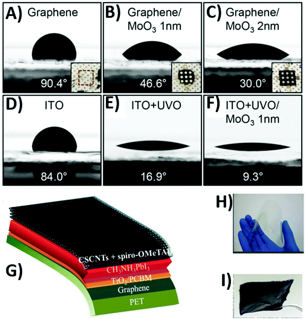 | ||
| Fig. 14 Droplets of PEDOT:PSS on (A) as-prepared graphene, (B) graphene covered with 1 nm MoO3, (C) graphene covered with 2 nm MoO3, (D) as-prepared ITO, (E) ITO treated with UV/O3, and (F) ITO covered with 1 nm MoO3 after UV/O3 treatment; the insets in (A–C) show the optical images of PEDOT:PSS/MAPbI3 films fabricated on the corresponding glass/graphene surfaces. (G) Device architecture of an all-carbon-electrode-based flexible PSC; (H) photograph of as-fabricated cross-stacking CNTs/PET; (I) photograph of as-fabricated cross-stacking graphene/PET. Adapted and reprinted with permission from ref. 217 and 220. | ||
A successful strategy for increasing the conductivity of carbon materials is nitrogen doping. In fact, the addition of lone pair electrons of nitrogen atoms can facilitate charge transfer. The nitrogen-doping of graphene for PSC application was performed by Zhu et al. in 2018.219 Nitrogen-doped graphene framework (NGF) was used as the cathode material and ensured a good network for charge transfer. PV parameters confirmed the increased properties of the NGF with respect to undoped samples. In fact, the PCE shifted from 8.98% to 10.32%, for pristine and NGF-based devices, respectively.
Finally, in a noteworthy work, Lou et al. used only carbon-based materials as electrodes for the fabrication of PSCs, as shown in Fig. 14G.220 In particular, graphene was chosen as the anode and was deposited on a poly(ethylene terephthalate) (PET) flexible substrate, due to its high transparency and flexibility; cross-stacking CNTs were used as the back electrode material, due to their high electrical conductivity. The optimum number of graphene layers was two, as reported by You.161 This double layer device demonstrated a Voc of 0.89 V, a Jsc of 20.25 mA cm−2, a FF of 0.65 and a PCE of 11.9%, and photographs of its components are shown in Fig. 14H and I.
4 Carbon nanotube-based back electrodes
CNTs are hollow cylinders resulting from the rolling up of a graphene layer. From their discovery in 1991,221 CNTs have attracted much attention in electronic and optoelectronic applications, due to their excellent charge transport ability, large hydrophobicity and high stability.222 CNTs are p-type semiconductors, with work functions ranging from −4.95 to −5.05 eV, suitable for working as back electrodes in PSCs. Their application in the PSC field has already been reviewed.75,213 Li et al. reported the first example of the use of CNTs as a back electrode in PSCs.160 They adopted an interfacial engineering method to improve the surface contact between CH3NH3PbI3 and CNTs: drops of toluene were added on the top of CNT film after the deposition onto the perovskite phase. Toluene did not dissolve any phase, but wetted the surface of both films, driving CNTs toward CH3NH3PbI3. PL quenching confirmed the strong adhesion through van der Waals interactions between the two films. As a result, this cell was able to convert solar radiation with a PCE of 6.87%.Device performance can be dramatically increased by using MWCNTs,223 consisting of several CNTs stacked together providing a continuous and homogeneous film, strongly attached to the perovskite surface. This represents a strong advantage over other carbon-based materials, such as carbon black, which forms a loosely packed film easy to be cracked. Graphite forms a uniform layer too, but the larger particles do not lead to a perfect contact with the perovskite phase. In a HTM-free device, the use of MWCNTs as a back electrode provided a PCE of 10.30%.223
Zheng et al. made a further effort toward the optimization of MWCNTs for PSC application,224 starting from the idea that the work function of MWCTNs (−4.46 eV) was still too high compared with the VB of the perovskite. As already mentioned before,157 the boron-doping of carbon-based materials is a suitable strategy to reduce their work function. Boron-doped MWCNTs were obtained by the reaction of MWCNTs with boric acid and subsequent thermal treatment, as shown in Fig. 15A. The product showed the same structure of MWCNTs, suggesting that boron can replace carbon without any change in the graphitic structure, and the thermal annealing reduced the number of defects. MWCNT- and boron-doped MWCNT-based devices attained average PCE values of 10.70% and 14.60%, respectively. The dramatic increase in PCE was ascribed to the ameliorated band alignment and improved charge extraction ability of boron-doped samples, as depicted in the scheme shown in Fig. 15B.
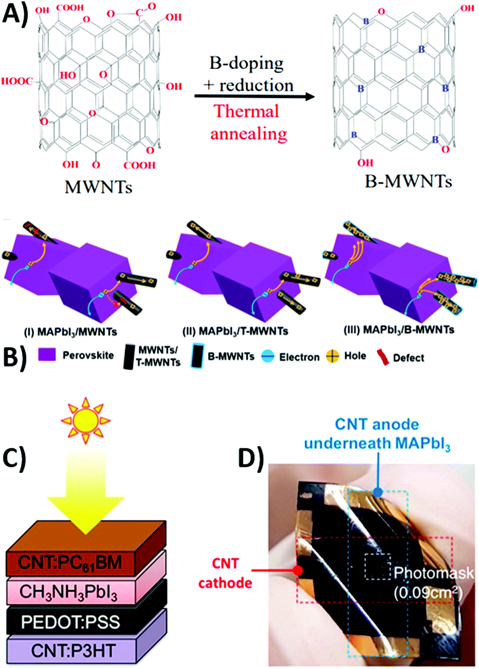 | ||
| Fig. 15 (A) Schematic structure of MWCNTs before and after boron-doping and thermal treatment; (B) schematic diagram of the stronger hole extraction and transport capability of boron-MWCNTs (right) with respect to pristine MWCNTs (left) and thermally treated MWCNTs (center). (C) Schematic architecture of a CNTs/PC61BM/CH3NH3PbI3/PEDOT:PSS/CNTs device and (D) digital picture of a PET-based device, highlighting its remarkable flexibility. Adapted and reprinted with permission from ref. 224 and 226. | ||
Like graphene,225 CNTs may also be exploited for the fabrication of transparent electrodes. In addition, their mechanical properties permit the use of flexible substrates, such as PET. In 2017 Jeon et al. demonstrated the use of CNTs as both front and back electrode materials.226 In these devices, the transparency of the electrode is fundamental to allow light reach the active material. In addition [6,6]-phenyl-C61-butyric acid methyl ester (PC61BM) and PEDOT:PSS were used as the ETM and HTM, respectively. This architecture (shown in Fig. 15C and D) was found to work well in both glass and PET-based flexible substrates, with a PCE of 7.3% and 7.1%, respectively.
As in the case of graphite and carbon black back electrodes, organic227–229 and inorganic149 HTMs have been exploited to further increase the hole extraction ability of CNTs.230,231 Aitola et al. reported a CNT-based PSC with spiro-OMeTAD as the HTM.228 An average PCE of 14.3% was achieved, still lower than that obtained with gold as the back electrode (18.4%). However, CNTs strongly increased the stability of the device at relatively high temperatures (60 °C): while the gold-based device degraded dramatically, exhibiting a loss of 20% in just 8 h, the CNT-based device was highly stable (loss of 0.04% in the same time). The migration of gold atoms and the penetration of air moisture were responsible for the degradation of the perovskite layer. On the other hand, these phenomena were suppressed by the use of hydrophobic CNTs.
P3HT is another suitable hydrophobic HTM for PSCs. It has already been used for graphite, carbon black and graphene electrodes.188,189 When used with CNTs, it acts as a strong crosslinker that binds together CNTs.227 Therefore, a uniform morphology and a network for charge transfer are obtained by using P3HT as an organic/polymeric HTM. With an optimized concentration of 2 mg mL−1 in the precursor solution, an average PCE of 12.54% was obtained (Voc = 0.90 V, Jsc = 22.21 mA cm−2, FF = 0.63).227 Below this concentration, the amount of P3HT was not enough to connect CNTs. On the other hand, above this concentration the excess of P3HT blocked the conductive pathway, increasing recombination phenomena.
A similar strategy involves the use of poly(ethylenimine) (PEI) in the CNT film.229 PEI played the important role of ameliorating the interface between carbon and PC61BM, the latter being used as an electron acceptor in inverted FTO/NiO/CH3NH3PbI3/PC61BM/CNTs:PEI architectures. The beneficial effect of PEI was demonstrated by the dramatic increase in PCE, i.e. 10.8% vs. 3.3% for the PEI-free device. This result was ascribed to the better contact and decreased energy barrier between CNTs and PC61BM.
Last, a p-type NiO semiconductor was demonstrated to work as a HTM in carbon-based PSCs.150–152,194 In 2017, Liu et al. reported the use of NiO as the HTM in fully printable CNT-based devices.149 The energy level of the NiO/CNTs composite matched well with that of the perovskite, ensuring a good hole extraction rate. The addition of NiO to the carbon material allowed the reduction of the thickness of the electrode (1.8 μm), while keeping the electrical conductivity constant. As a matter of fact, this device attained an average PCE of 12.7% (Voc = 0.945 V, Jsc = 20.7 mA cm−2, FF = 0.64), while the corresponding device with 1.8 μm-thick graphite achieved a PCE of only 6.2%.
5 Stability of carbon-based PSCs
This review has clearly highlighted that using noble metals is problematic and expensive, but the main drawback for the commercialization of PSCs is the poor long-term stability of the devices. Being carbon electrode-based devices the best performing architectures in terms of stability, this advantage will be further stressed in this section. Stability is a widely discussed topic in the PSC framework, and the authors of this review agree with the general opinion that tests carried out under maximum power point (MPP) conditions possess wider significance than the vast majority of shelf stability tests reported in the literature.232 Therefore, even though it was surprisingly noted that the vast majority of research groups proposed shelf stability tests for their carbon-based devices,233–324 this section highlights the most significant results achieved under MPP conditions.Bashir et al. investigated the stability of a HTM-free device fabricated with a thin layer of copper-doped nickel oxide (Cu:NiOx) NPs, which helped in improving the photocurrent and reducing the recombination resistance.325 MPP tracking was performed and the output current density was monitored under continuous illumination with a constant applied bias of 0.62 V. The current remained above 20 mA cm−2 for more than 50 h, and the device showed no sign of degradation for 60 h (see Fig. 16A). Moreover, a slight increase in current was observed during the experiment, and this was attributed to the interaction of the perovskite layer with ambient humidity. These researchers also fabricated a monolithic perovskite module on a 100 cm2 glass substrate (active area = 70 cm2) and the champion device showed an impressive PCE of 12.1%.
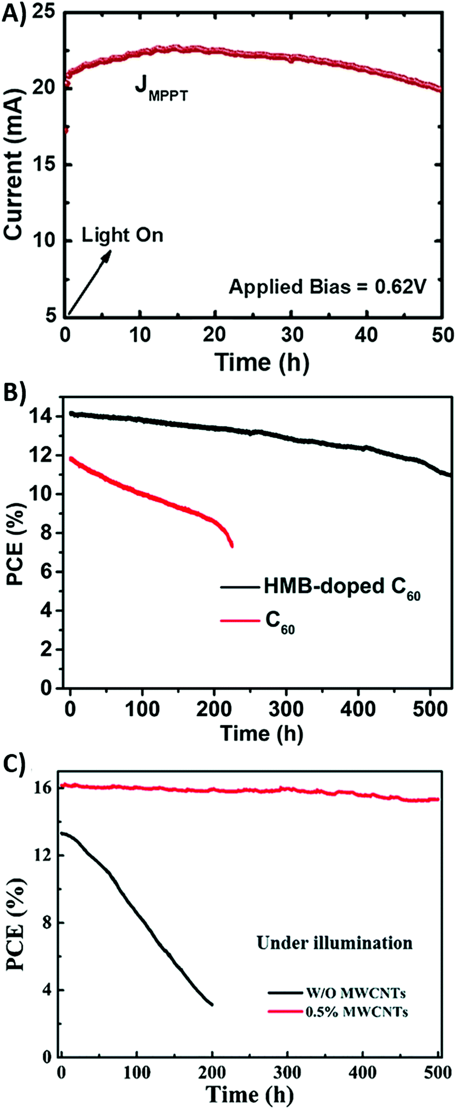 | ||
| Fig. 16 Aging tests at MPP under light for: (A) a PSC containing carbon and Cu:NiOx HTM; (B) C60- and HMB-doped C60 PSCs (with a 420 nm cut-off UV filter, under ambient conditions); (C) carbon-based PSCs with different MWCNT doping contents (in air with a RH of 30–80%). Adapted and reprinted with permission from ref. 325–327. | ||
Almost all of the carbon-based PSCs reported so far have been fabricated using TiO2 as the ETM, the latter requiring a high-temperature sintering process. As an alternative, Zhou et al. proposed solution-processed hexamethonium bromide (HMB)-doped C60 as the ETM, achieving a high PCE of over 16% without hysteresis.326 The remarkable stability of the resulting PSCs allows them to maintain nearly 90% of the initial performance after continuous operation for 338 h at MPP under 1 sun illumination in ambient air and with a 420 nm cut-off UV filter (see Fig. 16B).
Coupling carbon-based electrodes with all-air processing would truly lead to an easily upscalable PSC fabrication procedure. This goal was achieved by Zhou et al., who prepared MWCNT-incorporated FAxMA1−xPbIyBr3−y perovskite films in ambient air, where hydrophobic MWCNTs mediated the crystallization of the perovskite and prevented the erosion by moisture.327 With the low annealing temperature (<150 °C) adopted, a PCE of 16.25% was achieved and the photostability of the devices without encapsulation was studied by MPP tracking under continuous 1 sun illumination at a RH of 30–80%. Cells fabricated with 0.5% MWCNTs maintained 94.9% of the initial PCE after 500 h, while pristine devices retained only 23.4% after 200 h, as shown in Fig. 16C.
The self-adhesive macroporous carbon electrodes proposed by Zhang et al. and previously described in this review were subjected to an aging test under a N2 atmosphere, full AM1.5 sun-equivalent and UV-free conditions at the MPP.178 Gold-based PSCs suffered from much faster degradation due to the chemical reaction between the perovskite and gold, retaining just 22% of the initial PCE after 80 h (see Fig. 17A). Conversely, carbon-based devices exhibited a short rapid degradation and subsequent recovery, due to the improvement of the back contact between the electrode and spiro-OMeTAD; this phenomenon was attributed to an interface passivation caused by ion migration under illumination and an electric field. Carbon-based cells retained over 94% of the initial PCE, indicating greatly improved stability with respect to their gold-based counterparts.
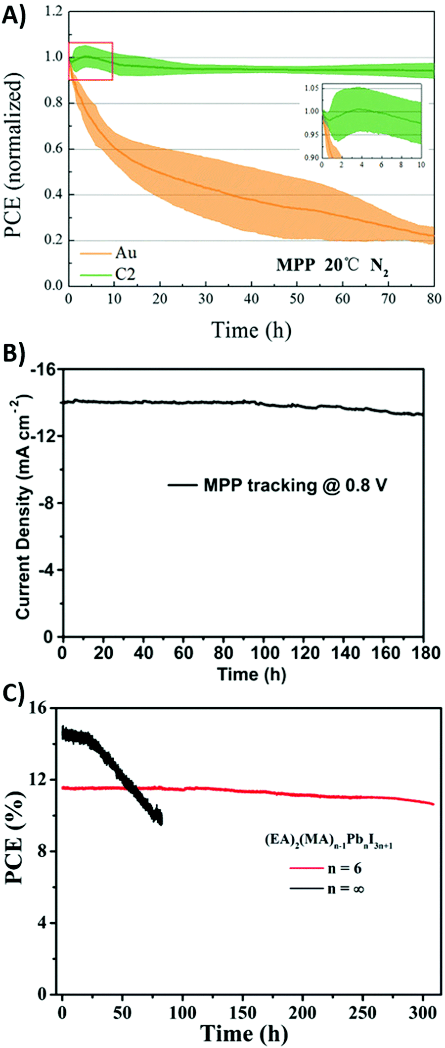 | ||
| Fig. 17 Aging tests at the MPP under light for: (A) gold- and carbon-based PSCs (the shaded area represents the standard deviation, and the inset shows the detailed degradation characteristics of carbon-based cells during the first 10 h); (B) C60-based PSC (with a 420 nm cut-off UV filter and RH of 40–60%); (C) (EA)2(MA)n−1PbnI3n+1 devices (n = 6, ∞) (RH of 30–80%). Adapted and reprinted with permission from ref. 60, 178 and 328. | ||
Meng et al. fabricated a carbon-based PSC without a HTM and using C60 as the ETM, reaching a PCE of 15.38% without hysteresis.328 Besides improved electron extraction, suppressed charge recombination and reduced sub-bandgap states at the C60/MAPbI3 interface, the device showed moisture and ion migration resistance. As shown in Fig. 17B, the long-term stability was tested under continuous 1 sun illumination (with a 420 nm UV filter) at the MPP, and the devices assembled without any encapsulation retained 95% of their initial performance after 180 h in air, with a RH of 40–60%.
Since the commonly used MAPbI3 photoabsorber is ambient-unstable and incompatible with the low-cost mass-production of carbon-based PSCs, Zhou et al. fabricated (EA)2(MA)n−1PbnI3n+1 films (n = 20, 10, 6) and assembled ITO/C60/(EA)2(MA)n−1PbnI3n+1/C devices with PCE exceeding 11.88%.60 The photostability was assessed without encapsulation, by MPP tracking under continuous 1 sun illumination (without a cut-off UV filter) in air with a RH of 30–80%. The PCE was retained at 91.8% after 308 h, while that of the reference cell fabricated with MAPbI3 dropped to 66.5% of the initial value after 83 h, as shown in Fig. 17C.
The inorganic interlayer of spinel Co3O4 used by Bashir et al. to suppress charge recombination and extract holes efficiently, and described in the previous sections of this review, was further investigated in aging tests at the MPP.158 A slight increase in Jsc was observed (see Fig. 18A), attributed to the interaction of the perovskite layer with ambient humidity, and the perovskite modules showed a degradation lower than 10% after continuous light soaking for 140 h.
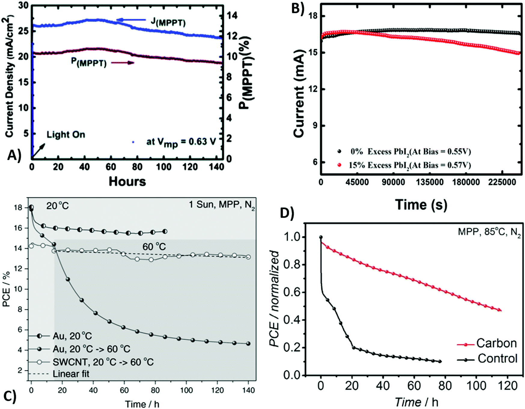 | ||
| Fig. 18 Aging tests at the MPP under light for: (A) a Co3O4/carbon solar cell; (B) carbon-based PSC with or without PbI2 excess; (C) gold- and single-walled CNT-contacted devices at elevated temperatures; (D) carbon cloth- and gold-based cells (under a N2 atmosphere, 85 °C). Adapted and reprinted with permission from ref. 158, 228, 329 and 330. | ||
Excess PbI2 is commonly considered as a way to boost the PCE in standard PSCs, and Kapoor et al. checked this issue in fully printable carbon-based devices.329 An improvement in Voc was detected, while other parameters remained unchanged. Continuous simulated solar illumination under ambient conditions (25°C and 65% RH) and the MPP was carried out for 68 h. Fig. 18B shows that no decrease of current was detected for the standard device, whereas the current reduced by 10% for the device containing 15% excess PbI2.
A 140 h MPP tracking of gold- and single-walled CNT-contacted devices under illumination at 1 sun in a N2 atmosphere was carried out by Aitola et al.228 The cells were kept at 20 °C for the first 14 h, and the gold-based cell showed pronounced changes; then, a stabilization period occurred, which was not seen in high temperature experiments, where gold-based devices underwent an irreversible degradation process. Noteworthily, the CNT-based device exhibited only a small PCE drop in this region, as shown in Fig. 18C.
Carbon cloth and carbon fibers, widely used in DSSCs and batteries, replaced gold in a batch of PSCs proposed by Gholipour et al.330 The optimized device configuration led to a PCE of 14.8%. Long-term stability was studied under a N2 atmosphere, 85 °C, constant 1 sun illumination and MPP tracking. While the gold-based cell suffered from rapid degradation, retaining less than 20% of the initial PCE after 20 h and less than 10% after 65 h, the carbon-based cell retained close to half of the starting PCE after 115 h (see Fig. 18D). This slight degradation of the carbon-based cell was attributed to chemical reactions between spiro-OMeTAD+ and migrating I−, hampering the conductivity of the HTM and thus the solar cell performance.
Several articles among those mentioned in this section focused on aging tests based on external degradation agents (e.g., moisture, oxygen, etc.), but no insight into the intrinsic degradation vector from the perovskite itself (releasing reactive gases) or studies of the true chemical inertness properties of carbon layers were provided, along with comparison with reference molecular/polymer-based HTMs. For sure it can be stated that, in the absence of HTMs, 4-tert-butylpyridine and organic lithium salt additives (typically used to dope spiro-OMeTAD) will not diffuse into the perovskite layer or absorb water traces; this surely improves the intrinsic stability of carbon-based devices. As a further advantage, carbon is not prone to formation of metal halides as many metal electrodes used in the PSC field do, leading to high resistivity and iodide deficiency in the perovskite layer. Moreover, carbon has not been demonstrated to penetrate the semiconductor material, while it is well known in the PSC community that Au diffuses through the perovskite. To further strengthen the solidity of carbon-based back electrodes in HTM-free devices, in situ analytical studies upon aging, highlighting the intrinsic stability of cell components, are required.
6 Conclusions
This review has summarized the most significant outcomes on PSC fabrication, characterization and scale up when carbon-based back electrodes are used. These platforms, prepared with graphite, carbon black, graphene or CNTs, exhibited significantly high stability, especially due to the high water resistance property of carbon. Research groups have proposed several processing routes, from scalable screen-printing approaches to inkjet printing, slot-die coating, and electrodeposition. The main trend in the literature scenario highlights that the PCE values of carbon electrode-based PSCs are lower than those of their gold-based counterparts, and the main reason lies in the poor contact at the perovskite/electrode interface; as secondary issues, resistance of carbon electrodes and charge recombination phenomena also contribute to lower Jsc and FF values.As a solution, current trends highlighted in this review show that interfacial engineering of carbon-based PSCs is becoming a fruitful research field, where scientists are working to decrease the heterogeneity in (opto)electronic properties of perovskites and carbon films and passivating their defects, thus boosting charge transfer and reducing recombination.
A further challenge in the long (but in rapid evolution) path towards gold-free PSCs will be the investigation behind the markedly improved stability of carbon-based devices. Indeed, even though many groups have carried out long-term stability experiments, not much is understood on the relationship between the singular aging of internal interfaces and components, and to what extent they affect the overall device stability against different external stress sources.
Conflicts of interest
There are no conflicts to declare.Acknowledgements
Politecnico di Torino and Compagnia di San Paolo are acknowledged for the financial support through the project “Metti in rete la tua idea di ricerca” (PEPPY project).References
- A. Kojima, K. Teshima, Y. Shirai and T. Miyasaka, Organometal halide perovskites as visible-light sensitizers for photovoltaic cells, J. Am. Chem. Soc., 2009, 131, 6050–6051 CrossRef CAS PubMed.
- National Renewable Energy Laboratory, http://www.nrel.gov, accessed July 2019.
- J. Burschka, N. Pellet, S. J. Moon, R. Humphry-Baker, P. Gao, M. K. Nazeeruddin and M. Grätzel, Sequential deposition as a route to high-performance perovskite-sensitized solar cells, Nature, 2013, 499, 316–319 CrossRef CAS PubMed.
- M. Liu, M. B. Johnston and H. J. Snaith, Efficient planar heterojunction perovskite solar cells by vapour deposition, Nature, 2013, 501, 395–398 CrossRef CAS PubMed.
- H. S. Kim, C. R. Lee, J. H. Im, K. B. Lee, T. Moehl, A. Marchioro, S. J. Moon, R. Humphry-Baker, J. H. Yum, J. E. Moser, M. Grätzel and N. G. Park, Lead iodide perovskite sensitized all-solid-state submicron thin film mesoscopic solar cell with efficiency exceeding 9%, Sci. Rep., 2012, 2, 591 CrossRef PubMed.
- H. Zhou, Q. Chen, G. Li, S. Luo, T. B. Song, H. S. Duan, Z. Hong, J. You, Y. Liu and Y. Yang, Interface engineering of highly efficient perovskite solar cells, Science, 2014, 345, 542–546 CrossRef CAS PubMed.
- N. J. Jeon, J. H. Noh, Y. C. Kim, W. S. Yang, S. Ryu and S. I. Seok, Solvent engineering for high-performance inorganic-organic hybrid perovskite solar cells, Nat. Mater., 2014, 13, 897–903 CrossRef CAS PubMed.
- L. K. Ono, Y. Qi and S. F. Liu, Progress toward stable lead halide perovskite solar cells, Joule, 2018, 2, 1961–1990 CrossRef CAS.
- Y. Cai, L. Xie, Z. Zhang, Y. Zhou, H. Liu, X. Lu, X. Gao, J. Gao, L. Shu, S. Wu and J. Liu, Tuning the A-site cation and X-site anion composition of CH3NH3PbI3 perovskite material for efficient planar perovskite solar cells, Electrochim. Acta, 2019, 293, 371–379 CrossRef CAS.
- D. Zhao, J. Huang, R. Qin, G. Yang and J. Yu, Efficient visible–near-infrared hybrid perovskite:PbS quantum dot photodetectors fabricated using an antisolvent additive solution process, Adv. Opt. Mater., 2018, 6, 1800979 CrossRef.
- C. R. Kalaiselvi, N. Muthukumarasamy, D. Velauthapillai, M. Kang and T. S. Senthil, Importance of halide perovskites for next generation solar cells – A review, Mater. Lett., 2018, 219, 198–200 CrossRef CAS.
- A. R. B. Mohd Yusoff, P. Gao and M. K. Nazeeruddin, Recent progress in organohalide lead perovskites for photovoltaic and optoelectronic applications, Coord. Chem. Rev., 2018, 373, 258–294 CrossRef.
- M. H. Li, P. S. Shen, K. C. Wang, T. F. Guo and P. Chen, Inorganic p-type contact materials for perovskite-based solar cells, J. Mater. Chem. A, 2015, 3, 9011–9019 RSC.
- H. Liu, M. Wang, J. Bian, Y. Feng, Z. Wang, B. Zhang and Y. Shi, Enhanced stability of perovskite solar cells using hydrophobic organic fluoropolymer, Appl. Phys. Lett., 2018, 113, 023902 CrossRef.
- C. C. Boyd, R. Cheacharoen, T. Leijtens and M. D. McGehee, Understanding degradation mechanisms and improving stability of perovskite photovoltaics, Chem. Rev., 2019, 119, 3418–3451 CrossRef CAS PubMed.
- Z. Gao, Y. Zheng, Z. Wang and J. Yu, Improving the stability and efficiency of perovskite light-emitting diodes via an insulating layer of polyethylenimine ethoxylated, J. Lumin., 2018, 201, 359–363 CrossRef CAS.
- F. Zhang, D. H. Kim and K. Zhu, 3D/2D multidimensional perovskites: Balance of high performance and stability for perovskite solar cells, Curr. Opin. Electrochem., 2018, 11, 105–113 CrossRef CAS.
- P. Li, Y. Zhang, C. Liang, G. Xing, X. Liu, F. Li, X. Liu, X. Hu, G. Shao and Y. Song, Phase pure 2D perovskite for high-performance 2D–3D heterostructured perovskite solar cells, Adv. Mater., 2018, 30, 1805323 CrossRef PubMed.
- S. Song, R. Hill, K. Choi, K. Wojciechowski, S. Barlow, J. Leisen, H. J. Snaith, S. R. Marder and T. Park, Surface modified fullerene electron transport layers for stable and reproducible flexible perovskite solar cells, Nano Energy, 2018, 49, 324–332 CrossRef CAS.
- F. Bi, X. Zheng and C. Yam, First-principles study of mixed cation methylammonium–formamidinium hybrid perovskite, Acta Phys.-Chim. Sin., 2019, 35, 69–75 Search PubMed.
- C. Geng, S. Xu, H. Zhong, A. L. Rogach and W. Bi, Aqueous synthesis of methylammonium lead halide perovskite nanocrystals, Angew. Chem., Int. Ed., 2018, 57, 9650–9654 CrossRef CAS PubMed.
- F. Zhang, X. Yang, H. Wang, M. Cheng, J. Zhao and L. Sun, Structure engineering of hole-conductor free perovskite-based solar cells with low-temperature-processed commercial carbon paste as cathode, ACS Appl. Mater. Interfaces, 2014, 6, 16140–16146 CrossRef CAS PubMed.
- E. Kasparavicius, A. Magomedov, T. Malinauskas and V. Getautis, Long-term stability of the oxidized hole-transporting materials used in perovskite solar cells, Chem. – Eur. J., 2018, 24, 9910–9918 CrossRef CAS PubMed.
- F. Zhang, X. Yang, M. Cheng, J. Li, W. Wang, H. Wang and L. Sun, Engineering of hole-selective contact for low temperature-processed carbon counter electrode-based perovskite solar cells, J. Mater. Chem. A, 2015, 3, 24272–24280 RSC.
- X. Liang, Y. Cheng, X. Xu, R. Dong, D. Li, Z. Zhou, R. Wei, G. Dong, S. W. Tsang and J. C. Ho, Enhanced performance of perovskite solar cells based on vertical TiO2 nanotube arrays with full filling of CH3NH3PbI3, Appl. Surf. Sci., 2018, 451, 250–257 CrossRef CAS.
- G. J. Hedley, C. Quarti, J. Harwell, O. V. Prezhdo, D. Beljonne and I. D. W. Samuel, Hot-hole cooling controls the initial ultrafast relaxation in methylammonium lead iodide perovskite, Sci. Rep., 2018, 8, 8115 CrossRef PubMed.
- Z. Shi and A. H. Jayatissa, Perovskites-based solar cells: A review of recent progress, materials and processing methods, Materials, 2018, 11, 729 CrossRef PubMed.
- X. Meng, X. Cui, M. Rager, S. Zhang, Z. Wang, J. Yu, Y. W. Harn, Z. Kang, B. K. Wagner, Y. Liu, C. Yu, J. Qiu and Z. Lin, Cascade charge transfer enabled by incorporating edge-enriched graphene nanoribbons for mesostructured perovskite solar cells with enhanced performance, Nano Energy, 2018, 52, 123–133 CrossRef CAS.
- Z. Ku, Y. Rong, M. Xu, T. Liu and H. Han, Full printable processed mesoscopic CH3NH3PbI3/TiO2 heterojunction solar cells with carbon counter electrode, Sci. Rep., 2013, 3, 3132 CrossRef PubMed.
- X. Liu, P. Li, Y. Zhang, X. Hu, Y. Duan, F. Li, D. Li, G. Shao and Y. Song, High-efficiency perovskite solar cells based on self-assembly n-doped fullerene derivative with excellent thermal stability, J. Power Sources, 2019, 413, 459–466 CrossRef CAS.
- J. A. Christians, P. A. Miranda Herrera and P. V. Kamat, Transformation of the excited state and photovoltaic efficiency of CH3NH3PbI3 perovskite upon controlled exposure to humidified air, J. Am. Chem. Soc., 2015, 137, 1530–1538 CrossRef CAS PubMed.
- A. M. A. Leguy, Y. Hu, M. Campoy-Quiles, M. I. Alonso, O. J. Weber, P. Azarhoosh, M. Van Schilfgaarde, M. T. Weller, T. Bein, J. Nelson, P. Docampo and P. R. F. Barnes, Reversible hydration of CH3NH3PbI3 in films, single crystals, and solar cells, Chem. Mater., 2015, 27, 3397–3407 CrossRef CAS.
- N. O. Weiss, H. Zhou, L. Liao, S. Jiang, Y. Huang and X. Duan, Graphene: An Emerging Electronic Material, Adv. Mater., 2012, 24, 5782–5825 CrossRef CAS PubMed.
- J. A. Luceño-Sánchez, A. M. Díez-Pascual and R. P. Capilla, Materials for photovoltaics: State of art and recent developments, Int. J. Mol. Sci., 2019, 20(4), 976 CrossRef PubMed.
- Y. Sun, W. Zhang, H. Chi, Y. Liu, C. L. Hou and D. Fang, Recent development of graphene materials applied in polymer solar cell, Renewable Sustainable Energy Rev., 2015, 43, 973–980 CrossRef CAS.
- M. Sibiński, M. Jakubowska, K. Znajdek, M. Słoma and B. Guzowski, Carbon nanotube transparent conductive layers for solar cells applications, Opt. Appl., 2011, 41, 375–381 Search PubMed.
- C. Ciceroni, A. Agresti, A. Di Carlo and F. Brunetti, Graphene oxide for DSSC, OPV and perovskite stability, Future Semicond. Oxides Next-Gener. Sol. Cells, 2017, 503–531 Search PubMed.
- N. N. M. Radzir, S. A. Hanifah, A. Ahmad, N. H. Hassan and F. Bella, Effect of lithium bis(trifluoromethylsulfonyl)imide salt-doped UV-cured glycidyl methacrylate, J. Solid State Electrochem., 2015, 19, 3079–3085 CrossRef CAS.
- F. Bella, A. B. Muñoz-García, F. Colò, G. Meligrana, A. Lamberti, M. Destro, M. Pavone and C. Gerbaldi, Combined structural, chemometric, and electrochemical investigation of vertically aligned TiO2 nanotubes for Na-ion batteries, ACS Omega, 2018, 3, 8440–8450 CrossRef CAS PubMed.
- S. Suriyakumar, S. Gopi, M. Kathiresan, S. Bose, E. B. Gowd, J. R. Nair, N. Angulakshmi, G. Meligrana, F. Bella, C. Gerbaldi and A. M. Stephan, Metal organic framework laden poly(ethylene oxide) based composite electrolytes for all-solid-state Li-S and Li-metal polymer batteries, Electrochim. Acta, 2018, 285, 355–364 CrossRef CAS.
- L. Lefrançois Perreault, F. Colò, G. Meligrana, K. Kim, S. Fiorilli, F. Bella, J. R. Nair, C. Vitale-Brovarone, J. Florek, F. Kleitz and C. Gerbaldi, Spray-dried mesoporous mixed Cu-Ni oxide@graphene nanocomposite microspheres for high power and durable Li-ion battery anodes, Adv. Energy Mater., 2018, 8, 1802438 CrossRef.
- J. R. Nair, F. Colò, A. Kazzazi, M. Moreno, D. Bresser, R. Lin, F. Bella, G. Meligrana, S. Fantini, E. Simonetti, G. B. Appetecchi, S. Passerini and C. Gerbaldi, Room temperature ionic liquid (RTIL)-based electrolyte cocktails for safe, high working potential Li-based polymer batteries, J. Power Sources, 2019, 412, 398–407 CrossRef CAS.
- A. Scalia, F. Bella, A. Lamberti, C. Gerbaldi and E. Tresso, Innovative multipolymer electrolyte membrane designed by oxygen inhibited UV-crosslinking enables solid-state in plane integration of energy conversion and storage devices, Energy, 2019, 166, 789–795 CrossRef CAS.
- A. Pedico, A. Lamberti, A. Gigot, M. Fontana, F. Bella, P. Rivolo, M. Cocuzza and C. F. Pirri, High-performing and stable wearable supercapacitor exploiting rGO aerogel decorated with copper and molybdenum sulfides on carbon fibers, ACS Appl. Energy Mater., 2018, 1, 4440–4447 CrossRef CAS.
- T. N. Huan, D. A. Dalla Corte, S. Lamaison, D. Karapinar, L. Lutz, N. Menguy, M. Foldyna, S. H. Turren-Cruz, A. Hagfeldt, F. Bella, M. Fontecave and V. Mougel, Low-cost high-efficiency system for solar-driven conversion of CO2 to hydrocarbons, Proc. Natl. Acad. Sci. U. S. A., 2019, 116, 9735–9740 CAS.
- M. Falco, L. Castro, J. R. Nair, F. Bella, F. Bardé, G. Meligrana and C. Gerbaldi, UV-cross-linked composite polymer electrolyte for high-rate, ambient temperature lithium batteries, ACS Appl. Energy Mater., 2019, 2, 1600–1607 CrossRef CAS.
- M. Falco, C. Simari, C. Ferrara, J. R. Nair, G. Meligrana, F. Bella, I. Nicotera, P. Mustarelli, M. Winter and C. Gerbaldi, Understanding the effect of UV-induced cross-linking on the physicochemical properties of highly performing PEO/LiTFSI-based polymer electrolytes, Langmuir, 2019, 35, 8210–8219 CAS.
- K. Deng, Z. Liu, Y. Xin and L. Li, PbI2/CH3NH3Cl mixed precursor–induced micrometer-scale grain perovskite film and room-temperature film encapsulation toward high efficiency and stability of planar perovskite solar cells, Adv. Mater. Interfaces, 2018, 5, 1800499 CrossRef.
- M. Wang, X. Jiang, J. Bian, Y. Feng, C. Wang, Y. Huang, Y. Zhang and Y. Shi, High-performance and stable mesoporous perovskite solar cells via well crystallized FA0.85MA0.15Pb(I0.8Br0.2)3, ACS Appl. Mater. Interfaces, 2019, 11, 2989–2996 CrossRef CAS PubMed.
- I. García-Benito, I. Zimmermann, J. Urieta-Mora, J. Aragó, J. Calbo, J. Perles, A. Serrano, A. Molina-Ontoria, E. Ortí, N. Martín and M. K. Nazeeruddin, Heteroatom effect on star-shaped hole-transporting materials for perovskite solar cells, Adv. Funct. Mater., 2018, 28, 1801734 CrossRef.
- Z. Zhang, W. Fu, H. Ding, H. X. Ju, K. Yan, X. Zhang, F. Ding, C. Z. Li and H. Chen, Modulate molecular interaction between hole extraction polymers and lead ions toward hysteresis-free and efficient perovskite solar cells, Adv. Mater. Interfaces, 2018, 5, 1800090 CrossRef.
- Y. Chen, Q. Meng, L. Zhang, C. Han, H. Gao, Y. Zhang and H. Yan, SnO2-based electron transporting layer materials for perovskite solar cells: A review of recent progress, J. Energy Chem., 2019, 35, 144–167 CrossRef.
- B. Roose and R. H. Friend, Extrinsic electron concentration in SnO2 electron extracting contact in lead halide perovskite solar cells, Adv. Mater. Interfaces, 2019, 6, 1801788 CrossRef.
- C. Zhen, T. Wu, R. Chen, L. Wang, G. Liu and H. M. Cheng, Strategies for modifying TiO2 based electron transport layers to boost perovskite solar cells, ACS Sustainable Chem. Eng., 2019, 7, 4586–4618 CrossRef CAS.
- M. I. H. Ansari, A. Qurashi and M. K. Nazeeruddin, Frontiers, opportunities, and challenges in perovskite solar cells: A critical review, J. Photochem. Photobiol., C, 2018, 35, 1–24 CrossRef CAS.
- I. Jeong, J. W. Jo, S. Bae, H. J. Son and M. J. Ko, A fluorinated polythiophene hole-transport material for efficient and stable perovskite solar cells, Dyes Pigm., 2019, 164, 1–6 CrossRef CAS.
- D. Zou, F. Yang, Q. Zhuang, M. Zhu, Y. Chen, G. You, Z. Lin, H. Zhen and Q. Ling, Perylene diimide-based electron-transporting material for perovskite solar cells with undoped poly(3-hexylthiophene) as hole-transporting material, ChemSusChem, 2019, 12, 1155–1161 CrossRef CAS PubMed.
- H. Chen and S. Yang, Carbon-based perovskite solar cells without hole transport materials: The front runner to the market?, Adv. Mater., 2017, 29, 1603994 CrossRef PubMed.
- C. Liu, J. Tu, X. Hu, Z. Huang, X. Meng, J. Yang, X. Duan, L. Tan, Z. Li and Y. Chen, Enhanced hole transportation for inverted tin-based perovskite solar cells with high performance and stability, Adv. Funct. Mater., 2019, 29, 1808059 CrossRef.
- J. Zhou, Z. Ye, J. Hou, J. Wu, Y. Z. Zheng and X. Tao, Efficient ambient-air-stable HTM-free carbon-based perovskite solar cells with hybrid 2D-3D lead halide photoabsorbers, J. Mater. Chem. A, 2018, 6, 22626–22635 RSC.
- T. N. W. J. Bandara, C. S. Knee, M. Furlani, I. Albinsson and B. E. Mellander, Novel photo-voltaic device based on Bi1−xLaxFeO3 perovskite films with higher efficiency, J. Mater. Sci.: Mater. Electron., 2019, 30, 1654–1662 CrossRef CAS.
- E. L. Dong, M. D. Gao, S. W. Yang, L. N. Zhang, H. Lyu, W. Zhang and J. W. Ma, Research on efficiency and stability of perovskite solar cells, J. Synth. Cryst., 2017, 46, 908–914 CAS.
- J. M. Yang, Y. Luo, Q. Bao, Y. Q. Li and J. X. Tang, Recent advances in energetics and stability of metal halide perovskites for optoelectronic applications, Adv. Mater. Interfaces, 2019, 6, 1801351 CrossRef.
- G. Grancini and M. K. Nazeeruddin, Dimensional tailoring of hybrid perovskites for photovoltaics, Nat. Rev. Mater., 2019, 4, 4–22 CrossRef CAS.
- Y. Liu, F. Li, Q. Li, K. Yang, T. Guo, X. Li and X. Zeng, Emissions at perovskite quantum dot/film interface with halide anion exchange, ACS Photonics, 2018, 5, 4504–4512 CrossRef CAS.
- T. A. Berhe, W. N. Su, C. H. Chen, C. J. Pan, J. H. Cheng, H. M. Chen, M. C. Tsai, L. Y. Chen, A. A. Dubale and B. J. Hwang, Organometal halide perovskite solar cells: Degradation and stability, Energy Environ. Sci., 2016, 9, 323–356 RSC.
- C. Wu, K. Wang, X. Feng, Y. Jiang, D. Yang, Y. Hou, Y. Yan, M. Sanghadasa and S. Priya, Ultrahigh durability perovskite solar cells, Nano Lett., 2019, 19, 1251–1259 CrossRef PubMed.
- L. Jiang, J. Lu, S. R. Raga, J. Sun, X. Lin, W. Huang, F. Huang, U. Bach and Y. B. Cheng, Fatigue stability of CH3NH3PbI3 based perovskite solar cells in day/night cycling, Nano Energy, 2019, 58, 687–694 CrossRef CAS.
- T. H. Schloemer, J. A. Christians, J. M. Luther and A. Sellinger, Doping strategies for small molecule organic hole-transport materials: Impacts on perovskite solar cell performance and stability, Chem. Sci., 2019, 10, 1904–1935 RSC.
- K. Aitola, K. Sveinbjörnsson, J. P. Correa-Baena, A. Kaskela, A. Abate, Y. Tian, E. M. J. Johansson, M. Grätzel, E. I. Kauppinen, A. Hagfeldt and G. Boschloo, Carbon nanotube-based hybrid hole-transporting material and selective contact for high efficiency perovskite solar cells, Energy Environ. Sci., 2016, 9, 461–466 RSC.
- N. H. Tiep, Z. Ku and H. J. Fan, Recent advances in improving the stability of perovskite solar cells, Adv. Energy Mater., 2016, 6, 1501420 CrossRef.
- S. D. Stranks, G. E. Eperon, G. Grancini, C. Menelaou, M. J. P. Alcocer, T. Leijtens, L. M. Herz, A. Petrozza and H. J. Snaith, Electron-hole diffusion lengths exceeding 1 micrometer in an organometal trihalide perovskite absorber, Science, 2013, 342, 341–344 CrossRef CAS PubMed.
- G. Xing, N. Mathews, S. Sun, S. S. Lim, Y. M. Lam, M. Graẗzel, S. Mhaisalkar and T. C. Sum, Long-range balanced electron-and hole-transport lengths in organic–inorganic CH3NH3PbI3, Science, 2013, 342, 344–347 CrossRef CAS PubMed.
- Y. Jiang, M. Remeika, Z. Hu, E. J. Juarez-Perez, L. Qiu, Z. Liu, T. Kim, L. K. Ono, D. Y. Son, Z. Hawash, M. R. Leyden, Z. Wu, L. Meng, J. Hu and Y. Qi, Negligible-Pb-waste and upscalable perovskite deposition technology for high-operational-stability perovskite solar modules, Adv. Energy Mater., 2019, 9, 1803047 CrossRef.
- Y. Cai, L. Liang and P. Gao, Promise of commercialization: Carbon materials for low-cost perovskite solar cells, Chin. Phys. B, 2018, 27, 018805 CrossRef.
- C. Phillips, A. Al-Ahmadi, S. J. Potts, T. Claypole and D. Deganello, The effect of graphite and carbon black ratios on conductive ink performance, J. Mater. Sci., 2017, 52, 9520–9530 CrossRef CAS.
- M. Hatala, P. Gemeiner, M. Hvojnik and M. Mikula, The effect of the ink composition on the performance of carbon-based conductive screen printing inks, J. Mater. Sci.: Mater. Electron., 2019, 30, 1034–1044 CrossRef CAS.
- T. Liu, L. Liu, M. Hu, Y. Yang, L. Zhang, A. Mei and H. Han, J. Power Sources, 2015, 293, 533–538 CrossRef CAS.
- Z. Meng, D. Guo, J. Yu and K. Fan, Appl. Surf. Sci., 2018, 430, 632–638 CrossRef CAS.
- J. Barichello, L. Vesce, F. Matteocci, E. Lamanna and A. Di Carlo, Sol. Energy Mater. Sol. Cells, 2019, 197, 76–83 CrossRef CAS.
- Y. Huang, L. Zhao, Y. Li, W. Li and S. Wang, Appl. Surf. Sci., 2019, 493, 975–981 CrossRef CAS.
- F. Meng, A. Liu, L. Gao, J. Cao, Y. Yan, N. Wang, M. Fan, G. Wei and T. Ma, Current progress in interfacial engineering of carbon-based perovskite solar cells, J. Mater. Chem. A, 2019, 7, 8690–8699 RSC.
- G. Niu, W. Li, J. Li, X. Liang and L. Wang, Enhancement of thermal stability for perovskite solar cells through cesium doping, RSC Adv., 2017, 7, 17473–17479 RSC.
- M. De Bastiani, E. Aydin, T. Allen, D. Walter, A. Fell, J. Peng, N. Gasparini, J. Troughton, D. Baran, K. Weber, T. P. White and S. De Wolf, Interfacial dynamics and contact passivation in perovskite solar cells, Adv. Electron. Mater., 2019, 5, 1800500 CrossRef.
- C. Ni, Z. Tie and Z. Jin, Solar cells based on all-inorganic halide perovskites: Progress and prospects, Trans. Nanjing Univ. Aeronaut. Astronaut., 2018, 35, 648–655 Search PubMed.
- J. Chen, W. Miu, J. Wang, G. Zheng and F. Long, A brief survey on the stability study of organometal halide perovskite solar cells, Mater. Rev., 2018, 32, 2151–2160 Search PubMed and 2175.
- L. Zhang, T. Liu, L. Liu, M. Hu, Y. Yang, A. Mei and H. Han, The effect of carbon counter electrodes on fully printable mesoscopic perovskite solar cells, J. Mater. Chem. A, 2015, 3, 9165–9170 RSC.
- C. Raminafshar, V. Dracopoulos, M. R. Mohammadi and P. Lianos, Carbon based perovskite solar cells constructed by screen-printed components, Electrochim. Acta, 2018, 276, 261–267 CrossRef CAS.
- T. Du, J. Kim, J. Ngiam, S. Xu, P. R. F. Barnes, J. R. Durrant and M. A. McLachlan, Elucidating the origins of subgap tail states and open-circuit voltage in methylammonium lead triiodide perovskite solar cells, Adv. Funct. Mater., 2018, 28, 1801808 CrossRef.
- I. Gelmetti, N. F. Montcada, A. Pérez-Rodríguez, E. Barrena, C. Ocal, I. García-Benito, A. Molina-Ontoria, N. Martín, A. Vidal-Ferran and E. Palomares, Energy alignment and recombination in perovskite solar cells: weighted influence on the open circuit voltage, Energy Environ. Sci., 2019, 12, 1309–1316 RSC.
- A. Mishra, Z. Ahmad, I. Zimmermann, D. Martineau, R. A. Shakoor, F. Touati, K. Riaz, S. A. Al-Muhtaseb and M. K. Nazeeruddin, Effect of annealing temperature on the performance of printable carbon electrodes for perovskite solar cells, Org. Electron., 2019, 65, 375–380 CrossRef CAS.
- C. Tian, A. Mei, S. Zhang, H. Tian, S. Liu, F. Qin, Y. Xiong, Y. Rong, Y. Hu, Y. Zhou, S. Xie and H. Han, Oxygen management in carbon electrode for high-performance printable perovskite solar cells, Nano Energy, 2018, 53, 160–167 CrossRef CAS.
- S. S. Mali, H. Kim, J. V. Patil and C. K. Hong, Bio-inspired carbon hole transporting layer derived from Aloe Vera plant for cost-effective fully printable mesoscopic carbon perovskite solar cells, ACS Appl. Mater. Interfaces, 2018, 10, 31280–31290 CrossRef CAS PubMed.
- M. Duan, Y. Rong, A. Mei, Y. Hu, Y. Sheng, Y. Guan and H. Han, Efficient hole-conductor-free, fully printable mesoscopic perovskite solar cells with carbon electrode based on ultrathin graphite, Carbon, 2017, 120, 71–76 CrossRef CAS.
- H. Tao, Y. Li, C. Zhang, K. Wang, J. Wang, B. Tan, L. Han and J. Tao, High permeable microporous structured carbon counter electrode assisted by polystyrene sphere for fully printable perovskite solar cells, Solid State Commun., 2018, 271, 71–75 CrossRef CAS.
- S. G. Hashmi, D. Martineau, M. I. Dar, T. T. T. Myllymäki, T. Sarikka, V. Ulla, S. M. Zakeeruddin and M. Grätzel, High performance carbon-based printed perovskite solar cells with humidity assisted thermal treatment, J. Mater. Chem. A, 2017, 5, 12060–12067 RSC.
- J. You, Z. Hong, T. B. Song, L. Meng, Y. Liu, C. Jiang, H. Zhou, W. H. Chang, G. Li and Y. Yang, Moisture assisted perovskite film growth for high performance solar cells, Appl. Phys. Lett., 2014, 105, 183902 CrossRef.
- H. Zheng, S. Dai, K. Zhou, G. Liu, B. Zhang, A. Alsaedi, T. Hayat and X. Pan, New-type highly stable 2D/3D perovskite materials: The effect of introducing ammonium cation on performance of perovskite solar cells, Sci. China Mater., 2019, 62, 508–518 CrossRef CAS.
- A. Mei, X. Li, L. Liu, Z. Ku, T. Liu, Y. Rong, M. Xu, M. Hu, J. Chen, Y. Yang, M. Grätzel and H. Han, A hole-conductor-free, fully printable mesoscopic perovskite solar cell with high stability, Science, 2014, 345, 295–298 CrossRef CAS PubMed.
- M. Hu, L. Liu, A. Mei, Y. Yang, T. Liu and H. Han, Efficient hole-conductor-free, fully printable mesoscopic perovskite solar cells with a broad light harvester NH2CH = NH2PbI3, J. Mater. Chem. A, 2014, 2, 17115–17121 RSC.
- D. Prochowicz, R. Runjhun, M. M. Tavakoli, P. Yadav, M. Saski, A. Q. Alanazi, D. J. Kubicki, Z. Kaszkur, S. M. Zakeeruddin, J. Lewinski and M. Grätzel, Engineering of perovskite materials based on formamidinium and cesium hybridization for high-efficiency solar cells, Chem. Mater., 2019, 31, 1620–1627 CrossRef CAS.
- N. Santhosh, S. R. Sitaaraman, P. Pounraj, R. Govindaraj, M. S. Pandian and P. Ramasamy, Fabrication of hole-transport-free perovskite solar cells using 5-ammonium valeric acid iodide as additive and carbon as counter electrode, Mater. Lett., 2019, 236, 706–709 CrossRef CAS.
- C. Xu, Z. Zhang, Y. Hu, Y. Sheng, P. Jiang, H. Han and J. Zhang, Printed hole-conductor-free mesoscopic perovskite solar cells with excellent long-term stability using PEAI as an additive, J. Energy Chem., 2018, 27, 764–768 CrossRef.
- Y. Kanemitsu and T. Handa, Photophysics of metal halide perovskites: From materials to devices, Jpn. J. Appl. Phys., 2018, 57, 090101 CrossRef.
- L. Liu, L. Deng, S. Huang, P. Zhang, J. Linnros, H. Zhong and I. Sychugov, Photodegradation of organometal hybrid perovskite nanocrystals: Clarifying the role of oxygen by single-dot photoluminescence, J. Phys. Chem. Lett., 2019, 10, 864–869 CrossRef CAS PubMed.
- H. Zhang, X. Ren, X. Chen, J. Mao, J. Cheng, Y. Zhao, Y. Liu, J. Milic, W. J. Yin, M. Grätzel and W. C. H. Choy, Improving the stability and performance of perovskite solar cells: Via off-the-shelf post-device ligand treatment, Energy Environ. Sci., 2018, 11, 2253–2262 RSC.
- S. Gholipour and M. Saliba, From exceptional properties to stability challenges of perovskite solar cells, Small, 2018, 14, 1802385 CrossRef PubMed.
- A. Magomedov, E. Kasparavicius, K. Rakstys, S. Paek, N. Gasilova, K. Genevicius, G. Juška, T. Malinauskas, M. K. Nazeeruddin and V. Getautis, Pyridination of hole transporting material in perovskite solar cells questions the long-term stability, J. Mater. Chem. C, 2018, 6, 8874–8878 RSC.
- N. Rolston, K. A. Bush, A. D. Printz, A. Gold-Parker, Y. Ding, M. F. Toney, M. D. McGehee and R. H. Dauskardt, Engineering stress in perovskite solar cells to improve stability, Adv. Energy Mater., 2018, 8, 1802139 CrossRef.
- M. Kim, S. G. Motti, R. Sorrentino and A. Petrozza, Enhanced solar cell stability by hygroscopic polymer passivation of metal halide perovskite thin film, Energy Environ. Sci., 2018, 11, 2609–2619 RSC.
- Z. Ahmad, T. Noma, S. Paek, K. T. Cho, D. Taguchi, M. Iwamoto, T. Manaka, M. K. Nazeeruddin, F. Touati and S. A. Al-Muhtaseb, Stability in 3D and 2D/3D hybrid perovskite solar cells studied by EFISHG and IS techniques under light and heat soaking, Org. Electron., 2019, 66, 7–12 CrossRef CAS.
- S. Emami, J. Martins, R. Madureira, D. Hernandez, G. Bernardo, J. Mendes and A. Mendes, Development of hermetic glass frit encapsulation for perovskite solar cells, J. Phys. D: Appl. Phys., 2019, 52, 074005 CrossRef.
- T. D. Siegler, D. W. Houck, S. H. Cho, D. J. Milliron and B. A. Korgel, Bismuth enhances the stability of CH3NH3PbI3 (MAPI) perovskite under high humidity, J. Phys. Chem. C, 2019, 123, 963–970 CrossRef CAS.
- H. Zhang, M. K. Nazeeruddin and W. C. H. Choy, Perovskite photovoltaics: The significant role of ligands in film formation, passivation, and stability, Adv. Mater., 2019, 31, 1805702 CrossRef PubMed.
- S. Wang, Y. Wang, Y. Zhang, X. Zhang, X. Shen, X. Zhuang, P. Lu, W. W. Yu, S. V. Kershaw and A. L. Rogach, Cesium lead chloride/bromide perovskite quantum dots with strong blue emission realized via a nitrate-induced selective surface defect elimination process, J. Phys. Chem. Lett., 2019, 10, 90–96 CrossRef CAS PubMed.
- T. Cai, F. Li, Y. Jiang, X. Liu, X. Xia, X. Wang, J. Peng, L. Wang and W. A. Daoud, In situ inclusion of thiocyanate for highly luminescent and stable CH3NH3PbBr3 perovskite nanocrystals, Nanoscale, 2019, 11, 1319–1325 RSC.
- M. Saliba, T. Matsui, J. Y. Seo, K. Domanski, J. P. Correa-Baena, M. K. Nazeeruddin, S. M. Zakeeruddin, E. Tress, A. Abate, A. Hagfeldt and M. Grätzel, Cesium-containing triple cation perovskite solar cells: Improved stability, reproducibility and high efficiency, Energy Environ. Sci., 2016, 9, 1989–1997 RSC.
- G. Liu, H. Zheng, X. Xu, L. Zhu, A. Alsaedi, T. Hayat, X. Pan and S. Dai, Efficient solar cells with enhanced humidity and heat stability based on benzylammonium–caesium–formamidinium mixed-dimensional perovskites, J. Mater. Chem. A, 2018, 6, 18067–18074 RSC.
- B. Billstrand, K. Bian, C. Karler, D. Ye, A. Hwang and H. Fan, Solution based synthesis of Cs4PbBr6 perovskite particles with high luminescence and stability, MRS Adv., 2018, 3, 2825–2831 CrossRef CAS.
- H. Bian, Q. Wang, S. Yang, C. Yan, H. Wang, L. Liang, Z. Jin, G. Wang and S. Liu, Nitrogen-doped graphene quantum dots for 80% photoluminescence quantum yield for inorganic γ-CsPbI3 perovskite solar cells with efficiency beyond 16%, J. Mater. Chem. A, 2019, 7, 5740–5747 RSC.
- B. Li, Y. Zhang, L. Fu, T. Yu, S. Zhou, L. Zhang and L. Yin, Surface passivation engineering strategy to fully-inorganic cubic CsPbI3 perovskites for high-performance solar cells, Nat. Commun., 2018, 9, 1076 CrossRef PubMed.
- J. Liang, C. Wang, Y. Wang, Z. Xu, Z. Lu, Y. Ma, H. Zhu, Y. Hu, C. Xiao, X. Yi, G. Zhu, H. Lv, L. Ma, T. Chen, Z. Tie, Z. Jin and J. Liu, All-inorganic perovskite solar cells, J. Am. Chem. Soc., 2016, 138, 15829–15832 CrossRef CAS PubMed.
- Z. Ahmad, A. S. Shikoh, S. Paek, M. K. Nazeeruddin, S. A. Al-Muhtaseb, F. Touati, J. Bhadra and N. J. Al-Thani, Degradation analysis in mixed (MAPbI3 and MAPbBr3) perovskite solar cells under thermal stress, J. Mater. Sci.: Mater. Electron., 2019, 30, 1354–1359 CrossRef CAS.
- C. Dokkhan, M. Z. Mokhtar, Q. Chen, B. R. Saunders, N. W. Hodson and B. Hamilton, Using microgels to control the morphology and optoelectronic properties of hybrid organic–inorganic perovskite films, Phys. Chem. Chem. Phys., 2018, 20, 27959–27969 RSC.
- I. Poli, J. Baker, J. McGettrick, F. De Rossi, S. Eslava, T. Watson and P. J. Cameron, Screen printed carbon CsPbBr3 solar cells with high open-circuit photovoltage, J. Mater. Chem. A, 2018, 6, 18677–18686 RSC.
- G. R. Yettapu, D. Talukdar, S. Sarkar, A. Swarnkar, A. Nag, P. Ghosh and P. Mandal, Terahertz conductivity within colloidal CsPbBr3 perovskite nanocrystals: Remarkably high carrier mobilities and large diffusion lengths, Nano Lett., 2016, 16, 4838–4848 CrossRef CAS PubMed.
- J. Chen and N. G. Park, Causes and solutions of recombination in perovskite solar cells, Adv. Mater. DOI:10.1002/adma.201803019.
- T. Zhang, Y. Hui, L. Chen, G. Li, B. Mao and Y. Zhao, Interfacial crosslinked quasi-2D perovskite with boosted carrier transport and enhanced stability, J. Phys. D: Appl. Phys., 2018, 51, 404001 CrossRef.
- F. Bella, D. Pugliese, J. R. Nair, A. Sacco, S. Bianco, C. Gerbaldi, C. Barolo and R. Bongiovanni, A UV-crosslinked polymer electrolyte membrane for quasi-solid dye-sensitized solar cells with excellent efficiency and durability, Phys. Chem. Chem. Phys., 2013, 15, 3706–3711 RSC.
- F. Bella, A. Lamberti, A. Sacco, S. Bianco, A. Chiodoni and R. Bongiovanni, Novel electrode and electrolyte membranes: towards flexible dye-sensitized solar cell combining vertically aligned TiO2 nanotube array and light-cured polymer network, J. Membr. Sci., 2014, 470, 125–131 CrossRef CAS.
- F. Bella, N. Vlachopoulos, K. Nonomura, S. M. Zakeeruddin, M. Grätzel, C. Gerbaldi and A. Hagfeldt, Direct light-induced polymerization of cobalt-based redox shuttles: an ultrafast way towards stable dye-sensitized solar cells, Chem. Commun., 2015, 51, 16308–16311 RSC.
- F. Bella, E. D. Ozzello, S. Bianco and R. Bongiovanni, Photo-polymerization of acrylic/methacrylic gel-polymer electrolyte membranes for dye-sensitized solar cells, Chem. Eng. J., 2013, 225, 873–879 CrossRef CAS.
- A. Sacco, F. Bella, S. De La Pierre, M. Castellino, S. Bianco, R. Bongiovanni and C. F. Pirri, Electrodes/electrolyte interfaces in the presence of a surface-modified photopolymer electrolyte: application in dye-sensitized solar cells, ChemPhysChem, 2015, 16, 960–969 CrossRef CAS PubMed.
- R. Shanti, F. Bella, Y. S. Salim, S. Y. Chee, S. Ramesh and K. Ramesh, Poly(methyl methacrylate-co-butyl acrylate-co-acrylic acid): physico-chemical characterization and targeted dye sensitized solar cell application, Mater. Des., 2016, 108, 560–569 CrossRef CAS.
- F. Bella, A. Sacco, G. Massaglia, A. Chiodoni, C. F. Pirri and M. Quaglio, Dispelling clichés at the nanoscale: the true effect of polymer electrolytes on the performance of dye-sensitized solar cells, Nanoscale, 2015, 7, 12010–12017 RSC.
- F. Bella, J. Popovic, A. Lamberti, E. Tresso, C. Gerbaldi and J. Maier, Interfacial effects in solid-liquid electrolytes for improved stability and performance of dye-sensitized solar cells, ACS Appl. Mater. Interfaces, 2017, 9, 37797–37803 CrossRef CAS PubMed.
- F. Bella, A. Verna and C. Gerbaldi, Patterning dye-sensitized solar cell photoanodes through a polymeric approach: a perspective, Mater. Sci. Semicond. Process., 2018, 73, 92–98 CrossRef CAS.
- F. Bella, A. Chiappone, J. R. Nair, G. Meligrana and C. Gerbaldi, Effect of different green cellulosic matrices on the performance of polymeric dye-sensitized solar cells, Chem. Eng. Trans., 2014, 41, 211–216 Search PubMed.
- D. Pintossi, G. Iannaccone, A. Colombo, F. Bella, M. Välimäki, K. L. Väisänen, J. Hast, M. Levi, C. Gerbaldi, C. Dragonetti, S. Turri and G. Griffini, Luminescent downshifting by photo-induced sol–gel hybrid coatings: accessing multifunctionality on flexible organic photovoltaics via ambient temperature material processing, Adv. Electron. Mater., 2016, 2, 1600288 CrossRef.
- F. Bella, P. Renzi, C. Cavallo and C. Gerbaldi, Caesium for perovskite solar cells: an overview, Chem. – Eur. J., 2018, 24, 12183–12205 CrossRef CAS PubMed.
- F. Bella, S. Galliano, G. Piana, G. Giacona, G. Viscardi, M. Grätzel, C. Barolo and C. Gerbaldi, Boosting the efficiency of aqueous solar cells: a photoelectrochemical estimation on the effectiveness of TiCl4 treatment, Electrochim. Acta, 2019, 302, 31–37 CrossRef CAS.
- Y. Rong, Z. Ku, A. Mei, T. Liu, M. Xu, S. Ko, X. Li and H. Han, Hole-conductor-free mesoscopic TiO2/CH3NH3PbI3 heterojunction solar cells based on anatase nanosheets and carbon counter electrodes, J. Phys. Chem. Lett., 2014, 5, 2160–2164 CrossRef CAS PubMed.
- L. Kavan, M. Grätzel, S. E. Gilbert, C. Klemenz and H. J. Scheel, Electrochemical and photoelectrochemical investigation of single-crystal anatase, J. Am. Chem. Soc., 1996, 118, 6716–6723 CrossRef CAS.
- L. Etgar, W. Zhang, S. Gabriel, S. G. Hickey, M. K. Nazeeruddin, A. Eychmüller, B. Liu and M. Grätzel, High efficiency quantum dot heterojunction solar cell using anatase (001) TiO2 nanosheets, Adv. Mater., 2012, 24, 2202–2206 CrossRef CAS PubMed.
- L. Etgar, P. Gao, Z. Xue, Q. Peng, A. K. Chandiran, B. Liu, M. K. Nazeeruddin and M. Grätzel, Mesoscopic CH3NH3PbI3/TiO2 heterojunction solar cells, J. Am. Chem. Soc., 2012, 134, 17396–17399 CrossRef CAS PubMed.
- J. Zhang, Z. Meng, D. Guo, H. Zou, J. Yu and K. Fan, Hole-conductor-free perovskite solar cells prepared with carbon counter electrode, Appl. Surf. Sci., 2018, 430, 531–538 CrossRef CAS.
- Z. Zolfaghari, E. Hassanabadi, D. Pitarch-Tena, S. J. Yoon, Z. Shariatinia, J. Van De Lagemaat, J. M. Luther and I. Mora-Seró, Operation mechanism of perovskite quantum dot solar cells probed by impedance spectroscopy, ACS Energy Lett., 2019, 4, 251–258 CrossRef CAS.
- L. Liu, A. Mei, T. Liu, P. Jiang, Y. Sheng, L. Zhang and H. Han, Fully printable mesoscopic perovskite solar cells with organic silane self-assembled monolayer, J. Am. Chem. Soc., 2015, 137, 1790–1793 CrossRef CAS PubMed.
- S. Liu, K. Cao, H. Li, J. Song, J. Han, Y. Shen and M. Wang, Full printable perovskite solar cells based on mesoscopic TiO2/Al2O3/NiO (carbon nanotubes) architecture, Sol. Energy, 2017, 144, 158–165 CrossRef CAS.
- K. Cao, Z. Zuo, J. Cui, Y. Shen, T. Moehl, S. M. Zakeeruddin, M. Grätzel and M. Wang, Efficient screen printed perovskite solar cells based on mesoscopic TiO2/Al2O3/NiO/carbon architecture, Nano Energy, 2015, 17, 171–179 CrossRef CAS.
- X. Xu, Z. Liu, Z. Zuo, M. Zhang, Z. Zhao, Y. Shen, H. Zhou, Q. Chen, Y. Yang and M. Wang, Hole selective NiO contact for efficient perovskite solar cells with carbon electrode, Nano Lett., 2015, 15, 2402–2408 CrossRef CAS PubMed.
- F. Behrouznejad, C. M. Tsai, S. Narra, E. W. G. Diau and N. Taghavinia, Interfacial investigation on printable carbon-based mesoscopic perovskite solar cells with NiOx/C back electrode, ACS Appl. Mater. Interfaces, 2017, 9, 25204–25215 CrossRef CAS PubMed.
- P. Jiang, Y. Xiong, M. Xu, A. Mei, Y. Sheng, L. Hong, T. W. Jones, G. J. Wilson, S. Xiong, D. Li, Y. Hu, Y. Rong and H. Han, The influence of the work function of hybrid carbon electrodes on printable mesoscopic perovskite solar cells, J. Phys. Chem. C, 2018, 122, 16481–16487 CrossRef CAS.
- Y. A. Kim, K. Fujisawa, H. Muramatsu, T. Hayashi, M. Endo, T. Fujimori, K. Kaneko, M. Terrones, J. Behrends, A. Eckmann, C. Casiraghi, K. S. Novoselov, R. Saito and M. S. Dresselhaus, Raman spectroscopy of boron-doped single-layer graphene, ACS Nano, 2012, 6, 6293–6300 CrossRef CAS PubMed.
- D. L. Carroll, P. Redlich, X. Blase, J. C. Charlier, S. Curran, S. Roth, P. M. Ajayan and M. Rühle, Effects of nanodomain formation on the electronic structure of doped carbon nanotubes, Phys. Rev. Lett., 1998, 81, 2332–2335 CrossRef CAS.
- L. S. Panchakarla, K. S. Subrahmanyam, S. K. Saha, A. Govindaraj, H. R. Krishnamurthy, U. V. Waghmare and C. N. R. Rao, Synthesis, structure, and properties of boron- and nitrogen-doped graphene, Adv. Mater., 2009, 21, 4726–4730 CAS.
- M. Duan, C. Tian, Y. Hu, A. Mei, Y. Rong, Y. Xiong, M. Xu, Y. Sheng, P. Jiang, X. Hou, X. Zhu, F. Qin and H. Han, Boron-doped graphite for high work function carbon electrode in printable hole-conductor-free mesoscopic perovskite solar cells, ACS Appl. Mater. Interfaces, 2017, 9, 31721–31727 CrossRef CAS PubMed.
- A. Bashir, S. Shukla, J. H. Lew, S. Shukla, A. Bruno, D. Gupta, T. Baikie, R. Patidar, Z. Akhter, A. Priyadarshi, N. Mathews and S. G. Mhaisalkar, Spinel Co3O4 nanomaterials for efficient and stable large area carbon-based printed perovskite solar cells, Nanoscale, 2018, 10, 2341–2350 RSC.
- G. E. Eperon, V. M. Burlakov, A. Goriely and H. J. Snaith, Neutral color semitransparent microstructured perovskite solar cells, ACS Nano, 2014, 8, 591–598 CrossRef CAS PubMed.
- Z. Li, S. A. Kulkarni, P. P. Boix, E. Shi, A. Cao, K. Fu, S. K. Batabyal, J. Zhang, Q. Xiong, L. H. Wong, N. Mathews and S. G. Mhaisalkar, Laminated carbon nanotube networks for metal electrode-free efficient perovskite solar cells, ACS Nano, 2014, 8, 6797–6804 CrossRef CAS PubMed.
- P. You, Z. Liu, Q. Tai, S. Liu and F. Yan, Efficient semitransparent perovskite solar cells with graphene electrodes, Adv. Mater., 2015, 27, 3632–3638 CrossRef CAS PubMed.
- F. R. Li, Y. Xu, W. Chen, S. H. Xie and J. Y. Li, Nanotube enhanced carbon grids as top electrodes for fully printable mesoscopic semitransparent perovskite solar cells, J. Mater. Chem. A, 2017, 5, 10374–10379 RSC.
- S. G. Hashmi, D. Martineau, X. Li, M. Ozkan, A. Tiihonen, M. I. Dar, T. Sarikka, S. M. Zakeeruddin, J. Paltakari, P. D. Lund and M. Grätzel, Air processed inkjet infiltrated carbon based printed perovskite solar cells with high stability and reproducibility, Adv. Mater. Technol., 2017, 2, 1600183 CrossRef.
- S. G. Hashmi, A. Tiihonen, D. Martineau, M. Ozkan, P. Vivo, K. Kaunisto, V. Ulla, S. M. Zakeeruddin and M. Grätzel, Long term stability of air processed inkjet infiltrated carbon-based printed perovskite solar cells under intense ultra-violet light soaking, J. Mater. Chem. A, 2017, 5, 4797–4802 RSC.
- N. U. Rahman, W. U. Khan, S. Khan, X. Chen, J. Khan, J. Zhao, Z. Yang, M. Wu and Z. Chi, A promising europium-based down conversion material: organic–inorganic perovskite solar cells with high photovoltaic performance and UV-light stability, J. Mater. Chem. A, 2019, 7, 6467–6474 RSC.
- A. K. Baranwal, S. Kanaya, T. A. N. Peiris, G. Mizuta, T. Nishina, H. Kanda, T. Miyasaka, H. Segawa and S. Ito, 100 °C thermal stability of printable perovskite solar cells using porous carbon counter electrodes, ChemSusChem, 2016, 9, 2604–2608 CrossRef CAS PubMed.
- F. De Rossi, J. A. Baker, D. Beynon, K. E. A. Hooper, S. M. P. Meroni, D. Williams, Z. Wei, A. Yasin, C. Charbonneau, E. H. Jewell and T. M. Watson, All printable perovskite solar modules with 198 cm2 active area and over 6% efficiency, Adv. Mater. Technol., 2018, 3, 1800156 CrossRef.
- F. J. Ramos, T. Maindron, S. Béchu, A. Rebai, M. Frégnaux, M. Bouttemy, J. Rousset, P. Schulz and N. Schneider, Versatile perovskite solar cell encapsulation by low-temperature ALD-Al2O3 with long-term stability improvement, Sustainable Energy Fuels, 2018, 2, 2468–2479 RSC.
- Z. Song, C. Wang, A. B. Phillips, C. R. Grice, D. Zhao, Y. Yu, C. Chen, C. Li, X. Yin, R. J. Ellingson, M. J. Heben and Y. Yan, Probing the origins of photodegradation in organic–inorganic metal halide perovskites with time-resolved mass spectrometry, Sustainable Energy Fuels, 2018, 2, 2460–2467 RSC.
- H. Zheng, G. Liu, X. Chen, B. Zhang, A. Alsaedi, T. Hayat, X. Pan and S. Dai, High-performance mixed-dimensional perovskite solar cells with enhanced stability against humidity, heat and UV light, J. Mater. Chem. A, 2018, 6, 20233–20241 RSC.
- N. U. Rahman, W. U. Khan, W. Li, S. Khan, J. Khan, S. Zheng, T. Su, J. Zhao, M. P. Aldred and Z. Chi, Simultaneous enhancement in performance and UV-light stability of organic-inorganic perovskite solar cells using a samarium-based down conversion material, J. Mater. Chem. A, 2019, 7, 322–329 RSC.
- T. J. Jacobsson, L. J. Schwan, M. Ottosson, A. Hagfeldt and T. Edvinsson, Determination of thermal expansion coefficients and locating the temperature-induced phase transition in methylammonium lead perovskites using X-ray diffraction, Inorg. Chem., 2015, 54, 10678–10685 CrossRef CAS PubMed.
- L. H. Chou, X. F. Wang, I. Osaka, C. G. Wu and C. L. Liu, Scalable ultrasonic spray-processing technique for manufacturing large-area CH3NH3PbI3 perovskite solar cells, ACS Appl. Mater. Interfaces, 2018, 10, 38042–38050 CrossRef CAS PubMed.
- Z. Wei, H. Chen, K. Yan and S. Yang, Inkjet printing and instant chemical transformation of a CH3NH3PbI3/nanocarbon electrode and interface for planar perovskite solar cells, Angew. Chem., Int. Ed., 2014, 53, 13239–13243 CrossRef CAS PubMed.
- H. Zhou, Y. Shi, Q. Dong, H. Zhang, Y. Xing, K. Wang, Y. Du and T. Ma, Hole-conductor-free, metal-electrode-free TiO2/CH3NH3PbI3 heterojunction solar cells based on a low-temperature carbon electrode, J. Phys. Chem. Lett., 2014, 5, 3241–3246 CrossRef CAS PubMed.
- H. Wei, J. Xiao, Y. Yang, S. Lv, J. Shi, X. Xu, J. Dong, Y. Luo, D. Li and Q. Meng, Free-standing flexible carbon electrode for highly efficient hole-conductor-free perovskite solar cells, Carbon, 2015, 93, 861–868 CrossRef CAS.
- Z. Liu, T. Shi, Z. Tang, B. Sun and G. Liao, Using a low-temperature carbon electrode for preparing hole-conductor-free perovskite heterojunction solar cells under high relative humidity, Nanoscale, 2016, 8, 7017–7023 RSC.
- H. Zhang, J. Xiao, J. Shi, H. Su, Y. Luo, D. Li, H. Wu, Y. B. Cheng and Q. Meng, Self-adhesive macroporous carbon electrodes for efficient and stable perovskite solar cells, Adv. Funct. Mater., 2018, 28, 1802985 CrossRef.
- N. Cheng, P. Liu, F. Qi, Y. Xiao, W. Yu, Z. Yu, W. Liu, S. S. Guo and X. Z. Zhao, Multi-walled carbon nanotubes act as charge transport channel to boost the efficiency of hole transport material free perovskite solar cells, J. Power Sources, 2016, 332, 24–29 CrossRef CAS.
- R. B. K. Siram, M. V. Khenkin, A. Niazov-Elkan, K. M. Anoop, H. Weissman, E. A. Katz, I. Visoly-Fisher and B. Rybtchinski, Hybrid organic nanocrystal/carbon nanotube film electrodes for air- and photo-stable perovskite photovoltaics, Nanoscale, 2019, 11, 3733–3740 RSC.
- H. Liu, X. Fu, W. Fu, B. Zong, L. Huang, H. Bala, S. Wang, Z. Guo, G. Sun, J. Cao and Z. Zhang, An effective TiO2 blocking layer for hole-conductor-free perovskite solar cells based on carbon counter electrode, Org. Electron., 2018, 59, 253–259 CrossRef CAS.
- H. Zhou, Y. Shi, K. Wang, Q. Dong, X. Bai, Y. Xing, Y. Du and T. Ma, Low-temperature processed and carbon-based ZnO/CH3NH3PbI3/C planar heterojunction perovskite solar cells, J. Phys. Chem. C, 2015, 119, 4600–4605 CrossRef CAS.
- Y. Jin and G. Chumanov, Solution-processed planar perovskite solar cell without a hole transport layer, ACS Appl. Mater. Interfaces, 2015, 7, 12015–12021 CrossRef CAS PubMed.
- X. Dou, D. Sabba, N. Mathews, L. H. Wong, Y. M. Lam and S. Mhaisalkar, Hydrothermal synthesis of high electron mobility Zn-doped SnO2 nanoflowers as photoanode material for efficient dye-sensitized solar cells, Chem. Mater., 2011, 23, 3938–3945 CrossRef CAS.
- S. Lin, B. Yang, X. Qiu, J. Yan, J. Shi, Y. Yuan, W. Tan, X. Liu, H. Huang, Y. Gao and C. Zhou, Efficient and stable planar hole-transport-material-free perovskite solar cells using low temperature processed SnO2 as electron transport material, Org. Electron., 2018, 53, 235–241 CrossRef CAS.
- H. Ye, Z. Liu, X. Liu, B. Sun, X. Tan, Y. Tu, T. Shi, Z. Tang and G. Liao, 17.78% efficient low-temperature carbon-based planar perovskite solar cells using Zn-doped SnO2 electron transport layer, Appl. Surf. Sci., 2019, 478, 417–425 CrossRef CAS.
- S. Zhao, J. Xie, G. Cheng, Y. Xiang, H. Zhu, W. Guo, H. Wang, M. Qin, X. Lu, J. Qu, J. Wang, J. Xu and K. Yan, General nondestructive passivation by 4-fluoroaniline for perovskite solar cells with improved performance and stability, Small, 2018, 14, 1803350 CrossRef PubMed.
- S. Mashhoun, Y. Hou, H. Chen, F. Tajabadi, N. Taghavinia, H. J. Egelhaaf and C. J. Brabec, Resolving a critical instability in perovskite solar cells by designing a scalable and printable carbon based electrode-interface architecture, Adv. Energy Mater., 2018, 8, 1802085 CrossRef.
- Q. Q. Chu, B. Ding, J. Peng, H. Shen, X. Li, Y. Liu, C. X. Li, C. J. Li, G. J. Yang, T. P. White and K. R. Catchpole, Highly stable carbon-based perovskite solar cell with a record efficiency of over 18% via hole transport engineering, J. Mater. Sci. Technol., 2019, 35, 987–993 CrossRef.
- F. Zhang, X. Yang, M. Cheng, W. Wang and L. Sun, Boosting the efficiency and the stability of low cost perovskite solar cells by using CuPc nanorods as hole transport material and carbon as counter electrode, Nano Energy, 2016, 20, 108–116 CrossRef CAS.
- J. Ren, J. Qu, J. Chen, Z. Li, Y. Cui, H. Wang, Z. Yu and Y. Hao, Fluorinated dopant-free hole-transporting material for efficient and stable perovskite solar cells with carbon cathode, J. Power Sources, 2018, 401, 29–36 CrossRef CAS.
- R. Hu, R. Zhang, Y. Ma, W. Liu, L. Chu, W. Mao, J. Zhang, J. Yang, Y. Pu and X. Li, Enhanced hole transfer in hole-conductor-free perovskite solar cells via incorporating CuS into carbon electrodes, Appl. Surf. Sci., 2018, 462, 840–846 CrossRef CAS.
- Y. Lv, Y. Guo, H. Zhang, X. Zhou and H. Chen, Enhanced efficiency and stability of fully air-processed TiO2 nanorods array based perovskite solar cell using commercial available CuSCN and carbon, Sol. Energy, 2018, 173, 7–16 CrossRef CAS.
- T. A. N. Peiris, A. K. Baranwal, H. Kanda, S. Fukumoto, S. Kanaya, L. Cojocaru, T. Bessho, T. Miyasaka, H. Segawa and S. Ito, Enhancement of the hole conducting effect of NiO by a N2 blow drying method in printable perovskite solar cells with low-temperature carbon as the counter electrode, Nanoscale, 2017, 9, 5475–5482 RSC.
- X. Jiang, D. Wang, Z. Yu, W. Ma, H. B. Li, X. Yang, F. Liu, A. Hagfeldt and L. Sun, Molecular engineering of copper phthalocyanines: A strategy in developing dopant-free hole-transporting materials for efficient and ambient-stable perovskite solar cells, Adv. Energy Mater., 2019, 9, 1803287 CrossRef.
- P. Qin, S. Tanaka, S. Ito, N. Tetreault, K. Manabe, H. Nishino, M. K. Nazeeruddin and M. Grätzel, Inorganic hole conductor-based lead halide perovskite solar cells with 12.4% conversion efficiency, Nat. Commun., 2014, 5, 3834 CrossRef CAS PubMed.
- A. W. Hains, Z. Liang, M. A. Woodhouse and B. A. Gregg, Molecular semiconductors in organic photovoltaic cells, Chem. Rev., 2010, 110, 6689–6735 CrossRef CAS PubMed.
- T. Stübinger and W. Brütting, Exciton diffusion and optical interference in organic donor–acceptor photovoltaic cells, J. Appl. Phys., 2001, 90, 3632–3641 CrossRef.
- M. Talarico, R. Termine, E. M. García-Frutos, A. Omenat, J. L. Serrano, B. Gómez-Lor and A. Golemme, New electrode-friendly triindole columnar phases with high hole mobility, Chem. Mater., 2008, 20, 6589–6591 CrossRef CAS.
- C. Kulshreshtha, G. W. Kim, R. Lampande, D. H. Huh, M. Chae and J. H. Kwon, New interfacial materials for rapid hole-extraction in organic photovoltaic cells, J. Mater. Chem. A, 2013, 1, 4077–4082 RSC.
- D. Y. Park, H. R. Byun, H. Kim, B. Kim and M. S. Jeong, Enhanced stability of perovskite solar cells using organosilane-treated double polymer passivation layers, J. Korean Phys. Soc., 2018, 73, 1787–1793 CrossRef CAS.
- K. D. Yuan, J. J. Wu, M. L. Liu, L. L. Zhang, F. F. Xu, L. D. Chen and F. Q. Huang, Fabrication and microstructure of p-type transparent conducting CuS thin film and its application in dye-sensitized solar cell, Appl. Phys. Lett., 2008, 93, 132106 CrossRef.
- K. Hooper, M. Carnie, C. Charbonneau and T. Watson, Near infrared radiation as a rapid heating technique for TiO2 films on glass mounted dye-sensitized solar cells, Int. J. Photoenergy, 2014, 2014, 953623 CrossRef.
- M. Rao, J. Fu, X. Wen, B. Sun, J. Wu, X. Liu and X. Dong, Near-infrared-excitable perovskite quantum dots: Via coupling with upconversion nanoparticles for dual-model anti-counterfeiting, New J. Chem., 2018, 42, 12353–12356 RSC.
- J. Baker, K. Hooper, S. Meroni, A. Pockett, J. McGettrick, Z. Wei, R. Escalante, G. Oskam, M. Carnie and T. Watson, High throughput fabrication of mesoporous carbon perovskite solar cells, J. Mater. Chem. A, 2017, 5, 18643–18650 RSC.
- H. Liu, X. Fu, W. Fu, B. Zong, L. Huang, H. Bala, S. Wang, Z. Guo, G. Sun, J. Cao and Z. Zhang, An effective TiO2 blocking layer for hole-conductor-free perovskite solar cells based on carbon counter electrode, Org. Electron., 2018, 59, 253–259 CrossRef CAS.
- J. A. Alberola-Borràs, J. A. Baker, F. De Rossi, R. Vidal, D. Beynon, K. E. A. Hooper, T. M. Watson and I. Mora-Seró, Perovskite photovoltaic modules: life cycle assessment of pre-industrial production process, iScience, 2018, 9, 542–551 CrossRef PubMed.
- E. L. Lim, C. C. Yap, M. H. H. Jumali, M. A. M. Teridi and C. H. Teh, A mini review: Can graphene be a novel material for perovskite solar cell applications?, Nano-Micro Lett., 2018, 10, 27 CrossRef PubMed.
- N. M. Julkapli and S. Bagheri, Graphene supported heterogeneous catalysts: An overview, Int. J. Hydrogen Energy, 2015, 40, 948–979 CrossRef CAS.
- Y. Shao, J. Wang, H. Wu, J. Liu, I. A. Aksay and Y. Lin, Graphene based electrochemical sensors and biosensors: A review, Electroanalysis, 2010, 22, 1027–1036 CrossRef CAS.
- F. Bonaccorso, Z. Sun, T. Hasan and A. C. Ferrari, Graphene photonics and optoelectronics, Nat. Photonics, 2010, 4, 611–622 CrossRef CAS.
- H. Kim and J. H. Ahn, Graphene for flexible and wearable device applications, Carbon, 2017, 120, 244–257 CrossRef CAS.
- C. Petridis, G. Kakavelakis and E. Kymakis, Renaissance of graphene-related materials in photovoltaics due to the emergence of metal halide perovskite solar cells, Energy Environ. Sci., 2018, 11, 1030–1061 RSC.
- K. Petridis, G. Kakavelakis, M. M. Stylianakis and E. Kymakis, Graphene-based inverted planar perovskite solar cells: Advancements, fundamental challenges, and prospects, Chem. – Asian J., 2018, 13, 240–249 CrossRef CAS PubMed.
- J. V. Milić, N. Arora, M. I. Dar, S. M. Zakeeruddin and M. Grätzel, Reduced graphene oxide as a stabilizing agent in perovskite solar cells, Adv. Mater. Interfaces, 2018, 5, 1800416 CrossRef.
- M. Acik and S. B. Darling, Graphene in perovskite solar cells: Device design, characterization and implementation, J. Mater. Chem. A, 2016, 4, 6185–6235 RSC.
- H. Sung, N. Ahn, M. S. Jang, J. K. Lee, H. Yoon, N. G. Park and M. Choi, Transparent conductive oxide-free graphene-based perovskite solar cells with over 17% efficiency, Adv. Energy Mater., 2016, 6, 1501873 CrossRef.
- J. Yoon, H. Sung, G. Lee, W. Cho, N. Ahn, H. S. Jung and M. Choi, Superflexible, high-efficiency perovskite solar cells utilizing graphene electrodes: Towards future foldable power sources, Energy Environ. Sci., 2017, 10, 337–345 RSC.
- Y. Zhu, S. Jia, J. Zheng, Y. Lin, Y. Wu and J. Wang, Facile synthesis of nitrogen-doped graphene frameworks for enhanced performance of hole transport material-free perovskite solar cells, J. Mater. Chem. C, 2018, 6, 3097–3103 RSC.
- Q. Luo, H. Ma, Q. Hou, Y. Li, J. Ren, X. Dai, Z. Yao, Y. Zhou, L. Xiang, H. Du, H. He, N. Wang, K. Jiang, H. Lin, H. Zhang and Z. Guo, All-carbon-electrode-based endurable flexible perovskite solar cells, Adv. Funct. Mater., 2018, 28, 1706777 CrossRef.
- S. Iijima, Helical microtubules of graphitic carbon, Nature, 1991, 354, 56–58 CrossRef CAS.
- S. N. Habisreutinger, R. J. Nicholas and H. J. Snaith, Carbon nanotubes in perovskite solar cells, Adv. Energy Mater., 2017, 7, 1601839 CrossRef.
- Z. Wei, H. Chen, K. Yan, X. Zheng and S. Yang, Hysteresis-free multi-walled carbon nanotube-based perovskite solar cells with a high fill factor, J. Mater. Chem. A, 2015, 3, 24226–24231 RSC.
- X. Zheng, H. Chen, Q. Li, Y. Yang, Z. Wei, Y. Bai, Y. Qiu, D. Zhou, K. S. Wong and S. Yang, Boron doping of multiwalled carbon nanotubes significantly enhances hole extraction in carbon-based perovskite solar cells, Nano Lett., 2017, 17, 2496–2505 CrossRef CAS PubMed.
- Z. Hosseini and T. Ghanbari, Designing an efficient graphene quantum dot-filled luminescent down shifting layer to improve the stability and efficiency of perovskite solar cells by simple optical modelling, RSC Adv., 2018, 8, 31502–31509 RSC.
- I. Jeon, S. Seo, Y. Sato, C. Delacou, A. Anisimov, K. Suenaga, E. I. Kauppinen, S. Maruyama and Y. Matsuo, Perovskite solar cells using carbon nanotubes both as cathode and as anode, J. Phys. Chem. C, 2017, 121, 25743–25749 CrossRef CAS.
- X. Zheng, H. Chen, Z. Wei, Y. Yang, H. Lin and S. Yang, High-performance, stable and low-cost mesoscopic perovskite (CH3NH3PbI3) solar cells based on poly(3-hexylthiophene)-modified carbon nanotube cathodes, Front. Optoelectron., 2016, 9, 71–80 CrossRef.
- K. Aitola, K. Domanski, J. P. Correa-Baena, K. Sveinbjörnsson, M. Saliba, A. Abate, M. Grätzel, E. Kauppinen, E. M. J. Johansson, W. Tress, A. Hagfeldt and G. Boschloo, High temperature-stable perovskite solar cell based on low-cost carbon nanotube hole contact, Adv. Mater., 2017, 29, 1606398 CrossRef PubMed.
- Y. Zhou, X. Yin, Q. Luo, X. Zhao, D. Zhou, J. Han, F. Hao, M. Tai, J. Li, P. Liu, K. Jiang and H. Lin, Efficiently improving the stability of inverted perovskite solar cells by employing polyethylenimine-modified carbon nanotubes as electrodes, ACS Appl. Mater. Interfaces, 2018, 10, 31384–31393 CrossRef CAS PubMed.
- A. Uddin, Perovskite solar cells, Mater. Energy, 2018, 12, 285–367 Search PubMed.
- C. C. Vidyasagar, B. M. Muñoz Flores and V. M. Jiménez Pérez, Recent advances in synthesis and properties of hybrid halide perovskites for photovoltaics, Nano-Micro Lett., 2018, 10, 68 CrossRef CAS PubMed.
- Q. Wang and A. Abate, Strategies toward stable perovskite solar cells, Adv. Mater. Interfaces, 2018, 5, 1800264 CrossRef.
- M. Tang, B. He, D. Dou, Y. Liu, J. Duan, Y. Zhao, H. Chen and Q. Tang, Toward efficient and air-stable carbon-based all-inorganic perovskite solar cells through substituting CsPbBr3 films with transition metal ions, Chem. Eng. J., 2019, 375, 121930 CrossRef CAS.
- Z. Liu, X. Liu, B. Sun, X. Tan, H. Ye, Y. Tu, T. Shi, Z. Tang and G. Liao, Fully low-temperature processed carbon-based perovskite solar cells using thermally evaporated cadmium sulfide as efficient electron transport layer, Org. Electron., 2019, 74, 152–160 CrossRef CAS.
- Y. Zhu, S. Wang, R. Ma and C. Wang, Enhanced efficiency and stability of inverted perovskite solar cells by carbon dots cathode interlayer via solution process, Org. Electron., 2019, 74, 228–236 CrossRef CAS.
- Y. Zhong, L. Xu, C. Li, B. Zhang and W. Wu, Needle coke: a predominant carbon black alternative for printable triple mesoscopic perovskite solar cells, Carbon, 2019, 153, 602–608 CrossRef CAS.
- G. Wang, J. Liu, K. Chen, R. Pathak, A. Gurung and Q. Qiao, High-performance carbon electrode-based CsPbI2Br inorganic perovskite solar cell based on poly(3-hexylthiophene)-carbon nanotubes composite hole-transporting layer, J. Colloid Interface Sci., 2019, 555, 180–186 CrossRef CAS PubMed.
- Y. Qiang, J. Cheng, Y. Qi, H. Shi, H. Liu, C. Geng and Y. Xie, Low-temperature preparation of HTM-free SnO2-based planar heterojunction perovskite solar cells with commercial carbon as counter electrode, J. Alloys Compd., 2019, 809, 151817 CrossRef CAS.
- L. Zhou, Y. Zuo, T. K. Mallick and S. Sundaram, Enhanced efficiency of carbon-based mesoscopic perovskite solar cells through a tungsten oxide nanoparticle additive in the carbon electrode, Sci. Rep., 2019, 9, 8778 CrossRef PubMed.
- C. Cai, K. Zhou, H. Guo, Y. Pei, Z. Hu, J. Zhang and Y. Zhu, Enhanced hole extraction by NiO nanoparticles in carbon-based perovskite solar cells, Electrochim. Acta, 2019, 312, 100–108 CrossRef CAS.
- Z. H. Liu, S. Bi, G. L. Hou, C. Z. Ying and X. J. Su, Dual-sized TiO2 nanoparticles as scaffold layers in carbon-based mesoscopic perovskite solar cells with enhanced performance, J. Power Sources, 2019, 430, 12–19 CrossRef CAS.
- Y. Yang, N. D. Pham, D. Yao, L. Fan, M. T. Hoang, V. T. Tiong, Z. Wang, H. Zhu and H. Wang, Interface engineering to eliminate hysteresis of carbon-based planar heterojunction perovskite solar cells via CuSCN incorporation, ACS Appl. Mater. Interfaces, 2019, 11, 28431–28441 CrossRef CAS PubMed.
- H. Li, S. Yang, S. Gong, J. Wu, S. Pan, Z. Chen, Q. Zhao, C. Shou and Q. Shen, Perovskite films with a sacrificial cation for solar cells with enhanced stability based on carbon electrodes, J. Alloys Compd., 2019, 797, 811–819 CrossRef CAS.
- G. Wang, W. Dong, A. Gurung, K. Chen, F. Wu, Q. He, R. Pathak and Q. Qiao, Improving photovoltaic performance of carbon-based CsPbBr3 perovskite solar cells by interfacial engineering using P3HT interlayer, J. Power Sources, 2019, 432, 48–54 CrossRef CAS.
- R. Subair, D. Di Girolamo, M. Bodik, V. Nadazdy, B. Li, P. Nadazdy, Z. Markovic, M. Benkovicova, J. Chlpik, M. Kotlar, Y. Halahovets, P. Siffalovic, M. Jergel, J. Tian, F. Brunetti and E. Majkova, Effect of the doping of PC61BM electron transport layer with carbon nanodots on the performance of inverted planar MAPbI3 perovskite solar cells, Sol. Energy, 2019, 189, 426–434 CrossRef CAS.
- X. Zhou, Y. Wang, C. Li and T. Wu, Doping amino-functionalized ionic liquid in perovskite crystal for enhancing performances of hole-conductor free solar cells with carbon electrode, Chem. Eng. J., 2019, 372, 46–52 CrossRef CAS.
- Z. Zhang, W. Fan, X. Wei, L. Zhang, Z. Yang, Z. Wei, T. Shen, H. Si and J. Qi, Promoted performance of carbon based perovskite solar cells by environmentally friendly additives of CH3COONH4 and Zn(CH3COO)2, J. Alloys Compd., 2019, 802, 694–703 CrossRef CAS.
- F. Zhao, Y. Guo, X. Wang, J. Tao, J. Jiang, Z. Hu and J. Chu, Enhanced performance of carbon-based planar CsPbBr3 perovskite solar cells with room-temperature sputtered Nb2O5 electron transport layer, Sol. Energy, 2019, 191, 263–271 CrossRef CAS.
- Y. Xiao, C. Wang, K. K. Kondamareddy, P. Liu, F. Qi, H. Zhang, S. Guo and X. Z. Zhao, Enhancing the performance of hole-conductor free carbon-based perovskite solar cells through rutile-phase passivation of anatase TiO2 scaffold, J. Power Sources, 2019, 422, 138–144 CrossRef CAS.
- Y. Feng, Q. Chen, L. Dong, Z. Zhang, C. Li, S. Yang, S. Cai and Z. X. Xu, Carbon-chain length substituent effects on Cu(II) phthalocyanines as dopant-free hole-transport materials for perovskite solar cells, Sol. Energy, 2019, 184, 649–656 CrossRef CAS.
- Z. Li, C. Liu, X. Zhang, J. Guo, H. Cui, L. Shen, Y. Bi and W. Guo, Using easily prepared carbon nanodots to improve hole transport capacity of perovskite solar cells, Mater. Today Energy, 2019, 12, 161–167 CrossRef.
- B. Zhang, W. Fu, X. Meng, A. Runa, P. Su and H. Yang, Improved crystallization of perovskite films using PbTiO3-decorated mesoporous scaffold layers for high stable carbon-counter-electrode solar cells, Org. Electron., 2019, 69, 164–173 CrossRef CAS.
- M. Yang, J. Li, J. Li, Z. Yuan, J. Zou, G. Lei, L. Zhao, X. Wang, B. Dong and S. Wang, High efficient and long-time stable planar heterojunction perovskite solar cells with doctor-bladed carbon electrode, J. Power Sources, 2019, 424, 61–67 CrossRef CAS.
- Q. Guo, F. Yuan, B. Zhang, S. Zhou, J. Zhang, Y. Bai, L. Fan, T. Hayat, A. Alsaedi and Z. Tan, Passivation of the grain boundaries of CH3NH3PbI3 using carbon quantum dots for highly efficient perovskite solar cells with excellent environmental stability, Nanoscale, 2019, 11, 115–124 RSC.
- Y. Wang, H. Zhao, Y. Mei, H. Liu, S. Wang and X. Li, Carbon nanotube bridging method for hole transport layer-free paintable carbon-based perovskite solar cells, ACS Appl. Mater. Interfaces, 2019, 11, 916–923 CrossRef CAS.
- Y. Ma, H. Zhang, Y. Zhang, R. Hu, M. Jiang, R. Zhang, H. Lv, J. Tian, L. Chu, J. Zhang, Q. Xue, H. L. Yip, R. Xia, X. Li and W. Huang, Enhancing the performance of inverted perovskite solar cells via grain boundary passivation with carbon quantum dots, ACS Appl. Mater. Interfaces, 2019, 11, 3044–3052 CrossRef CAS.
- A. K. Baranwal, H. Kanda, N. Shibayama, H. Masutani, T. A. N. Peiris, S. Kanaya, H. Segawa, T. Miyasaka and S. Ito, Thermal degradation analysis of sealed perovskite solar cell with porous carbon electrode at 100 °C for 7000 h, Energy Technol., 2019, 7, 245–252 CrossRef CAS.
- W. Chen, X. Yin, M. Que, H. Xie, J. Liu, C. Yang, Y. Guo, Y. Wu and W. Que, A comparative study of planar and mesoporous perovskite solar cells with printable carbon electrodes, J. Power Sources, 2019, 412, 118–124 CrossRef CAS.
- X. Liu, X. Tan, Z. Liu, H. Ye, B. Sun, T. Shi, Z. Tang and G. Liao, Boosting the efficiency of carbon-based planar CsPbBr3 perovskite solar cells by a modified multistep spin-coating technique and interface engineering, Nano Energy, 2019, 56, 184–195 CrossRef CAS.
- J. Yan, S. Lin, X. Qiu, H. Chen, K. Li, Y. Yuan, M. Long, B. Yang, Y. Gao and C. Zhou, Accelerated hole-extraction in carbon-electrode based planar perovskite solar cells by moisture-assisted post-annealing, Appl. Phys. Lett., 2019, 114, 103503 CrossRef.
- B. Zong, W. Fu, Z. A. Guo, S. Wang, L. Huang, B. Zhang, H. Bala, J. Cao, X. Wang, G. Sun and Z. Zhang, Highly stable hole-conductor-free perovskite solar cells based upon ammonium chloride and a carbon electrode, J. Colloid Interface Sci., 2019, 540, 315–321 CrossRef CAS.
- F. Meng, L. Gao, Y. Yan, J. Cao, N. Wang, T. Wang and T. Ma, Ultra-low-cost coal-based carbon electrodes with seamless interfacial contact for effective sandwich-structured perovskite solar cells, Carbon, 2019, 145, 290–296 CrossRef CAS.
- J. W. Lee, I. Jeon, H. S. Lin, S. Seo, T. H. Han, A. Anisimov, E. I. Kauppinen, Y. Matsuo, S. Maruyama and Y. Yang, Vapor-assisted ex-situ doping of carbon nanotube toward efficient and stable perovskite solar cells, Nano Lett., 2019, 19, 2223–2230 CrossRef CAS.
- C. Dong, X. Han, W. Li, Q. Qiu and J. Wang, Anti-solvent assisted multi-step deposition for efficient and stable carbon-based CsPbI2Br all-inorganic perovskite solar cell, Nano Energy, 2019, 59, 553–559 CrossRef CAS.
- P. Liu, Y. Gong, Y. Xiao, M. Su, S. Kong, F. Qi, H. Zhang, S. Wang, X. Sun, C. Wang and X. Z. Zhao, Highly efficient and stable air-processed hole-transport-material free carbon based perovskite solar cells with caesium incorporation, Chem. Commun., 2019, 55, 218–221 RSC.
- J. Liu, L. Zhu, S. Xiang, Y. Wei, M. Xie, H. Liu, W. Li and H. Chen, Growing high-quality CsPbBr3 by using porous CsPb2Br5 as an intermediate: a promising light absorber in carbon-based perovskite solar cells, Sustainable Energy Fuels, 2019, 3, 184–194 RSC.
- Z. Guo, S. Teo, Z. Xu, C. Zhang, Y. Kamata, S. Hayase and T. Ma, Achievable high: Voc of carbon based all-inorganic CsPbIBr2 perovskite solar cells through interface engineering, J. Mater. Chem. A, 2019, 7, 1227–1232 RSC.
- H. Zhang, H. Wang, Y. Yang, C. Hu, Y. Bai, T. Zhang, W. Chen and S. Yang, HxMoO3-y nanobelts: an excellent alternative to carbon electrodes for high performance mesoscopic perovskite solar cells, J. Mater. Chem. A, 2019, 7, 1499–1508 RSC.
- S. Wang, Y. Zhu, B. Liu, C. Wang and R. Ma, Introduction of carbon nanodots into SnO2 electron transport layer for efficient and UV stable planar perovskite solar cells, J. Mater. Chem. A, 2019, 7, 5353–5362 RSC.
- P. Wang, N. Chai, C. Wang, J. Hua, F. Huang, Y. Peng, J. Zhong, Z. Ku and Y. B. Cheng, Enhancing the thermal stability of the carbon-based perovskite solar cells by using a CsxFA1-xPbBrxI3-x light absorber, RSC Adv., 2019, 9, 11877–11881 RSC.
- X. Zhang, Y. Zhou, Y. Li, J. Sun, X. Lu, X. Gao, J. Gao, L. Shui, S. Wu and J. M. Liu, Efficient and carbon-based hole transport layer-free CsPbI2Br planar perovskite solar cells using PMMA modification, J. Mater. Chem. C, 2019, 7, 3852–3861 RSC.
- X. Zhu, J. Sun, S. Yuan, N. Li, Z. Qiu, J. Jia, Y. Liu, J. Dong, P. Lv and B. Cao, Efficient and stable planar perovskite solar cells with carbon quantum dots-doped PCBM electron transport layer, New J. Chem., 2019, 43, 7130–7135 RSC.
- X. Wu, L. Xie, K. Lin, J. Lu, K. Wang, W. Feng, B. Fan, P. Yin and Z. Wei, Efficient and stable carbon-based perovskite solar cells enabled by the inorganic interface of CuSCN and carbon nanotubes, J. Mater. Chem. A, 2019, 7, 12236–12243 RSC.
- J. Liu, Q. Zhou, N. K. Thein, L. Tian, D. Jia, E. M. J. Johansson and X. Zhang, In situ growth of perovskite stacking layers for high-efficiency carbon-based hole conductor free perovskite solar cells, J. Mater. Chem. A, 2019, 7, 13777–13786 RSC.
- J. Han, X. Yin, Y. Zhou, H. Nan, Y. Gu, M. Tai, J. Li and H. Lin, High efficient large-area perovskite solar cells based on paintable carbon electrode with NiO nanocrystal-carbon intermediate layer, Chem. Lett., 2019, 48, 734–737 CrossRef CAS.
- S. He, L. Qiu, D. Y. Son, Z. Liu, E. J. Juarez-Perez, L. K. Ono, C. Stecker and Y. Qi, Carbon-based electrode engineering boosts the efficiency of all low-temperature-processed perovskite solar cells, ACS Energy Lett., 2019, 9, 2032–2039 CrossRef.
- Y. Yang, Z. Liu, W. K. Ng, L. Zhang, H. Zhang, X. Meng, Y. Bai, S. Xiao, T. Zhang, C. Hu, K. S. Wong and S. Yang, An ultrathin ferroelectric perovskite oxide layer for high-performance hole transport material free carbon based halide perovskite solar cells, Adv. Funct. Mater., 2019, 29, 1806506 CrossRef.
- W. Zhu, Q. Zhang, D. Chen, Z. Zhang, Z. Lin, J. Chang, J. Zhang, C. Zhang and Y. Hao, Intermolecular exchange boosts efficiency of air-stable, carbon-based all-inorganic planar CsPbIBr2 perovskite solar cells to over 9%, Adv. Energy Mater., 2018, 8, 1802080 CrossRef.
- Y. Wei, W. Li, S. Xiang, J. Liu, H. Liu, L. Zhu and H. Chen, Precursor effects on methylamine gas-induced CH3NH3PbI3 films for stable carbon-based perovskite solar cells, Sol. Energy, 2018, 174, 139–148 CrossRef CAS.
- K. Li, H. Chen, H. Liu, Y. Yuan, Y. Gao, B. Yang and C. Zhou, Dependence of power conversion properties of the hole-conductor-free mesoscopic perovskite solar cells on the thickness of carbon film, Org. Electron., 2018, 62, 298–303 CrossRef CAS.
- A. Mashreghi and K. Maleki, Improving perovskite/carbon interfacial contact in carbon based perovskite solar cells by changing two-step spin coating sequence, Mater. Sci. Semicond. Process., 2018, 87, 92–99 CrossRef CAS.
- H. L. Hsu, H. T. Hsiao, T. Y. Juang, B. H. Jiang, S. C. Chen, R. J. Jeng and C. P. Chen, Carbon nanodot additives realize high-performance air-stable p–i–n perovskite solar cells providing efficiencies of up to 20.2%, Adv. Energy Mater., 2018, 8, 1802323 CrossRef.
- J. Han, X. Yin, Y. Zhou, H. Nan, Y. Gu, M. Tai, J. Li and H. Lin, Perovskite/poly[bis(4-phenyl)(2,4,6-trimethylphenyl)amine] bulk heterojunction for high-efficient carbon-based large-area solar cells by gradient engineering, ACS Appl. Mater. Interfaces, 2018, 10, 42328–42334 CrossRef CAS PubMed.
- J. Liang, Z. Liu, L. Qiu, Z. Hawash, L. Meng, Z. Wu, Y. Jiang, L. K. Ono and Y. Qi, Enhancing optical, electronic, crystalline, and morphological properties of cesium lead halide by Mn substitution for high-stability all-inorganic perovskite solar cells with carbon electrodes, Adv. Energy Mater., 2018, 8, 1800504 CrossRef.
- S. Xiang, Z. Fu, W. Li, Y. Wei, J. Liu, H. Liu, L. Zhu, R. Zhang and H. Chen, Highly air-stable carbon-based α-CsPbI3 perovskite solar cells with a broadened optical spectrum, ACS Energy Lett., 2018, 3, 1824–1831 CrossRef CAS.
- X. Liu, Z. Liu, B. Sun, X. Tan, H. Ye, Y. Tu, T. Shi, Z. Tang and G. Liao, All low-temperature processed carbon-based planar heterojunction perovskite solar cells employing Mg-doped rutile TiO2 as electron transport layer, Electrochim. Acta, 2018, 283, 1115–1124 CrossRef CAS.
- W. Zhu, Q. Zhang, C. Zhang, Z. Zhang, D. Chen, Z. Lin, J. Chang, J. Zhang and Y. Hao, Aged precursor solution toward low-temperature fabrication of efficient carbon-based all-inorganic planar CsPbIBr2 perovskite solar cells, ACS Appl. Energy Mater., 2018, 1, 4991–4997 CrossRef CAS.
- L. Chu, W. Liu, Z. Qin, R. Zhang, R. Hu, J. Yang, J. Yang and X. Li, Boosting efficiency of hole conductor-free perovskite solar cells by incorporating p-type NiO nanoparticles into carbon electrodes, Sol. Energy Mater. Sol. Cells, 2018, 178, 164–169 CrossRef CAS.
- J. Duan, T. Hu, Y. Zhao, B. He and Q. Tang, Carbon-electrode-tailored all-inorganic perovskite solar cells to harvest solar and water-vapor energy, Angew. Chem., Int. Ed., 2018, 57, 5746–5749 CrossRef CAS PubMed.
- V. D. Tran, S. V. N. Pammi, V. D. Dao, H. S. Choi and S. G. Yoon, Chemical vapor deposition in fabrication of robust and highly efficient perovskite solar cells based on single-walled carbon nanotubes counter electrodes, J. Alloys Compd., 2018, 747, 703–711 CrossRef CAS.
- Z. Liu, B. Sun, X. Liu, J. Han, H. Ye, T. Shi, Z. Tang and G. Liao, Efficient carbon-based CsPbBr3 inorganic perovskite solar cells by using Cu-phthalocyanine as hole transport material, Nano-Micro Lett., 2018, 10, 34 CrossRef PubMed.
- M. Shirazi, M. R. Toroghinejad, R. Sabet Dariani and M. T. Hosseinnejad, Fabrication of hole-conductor-free perovskite solar cells based on Al doped ZnO and low-cost carbon electrode, J. Mater. Sci.: Mater. Electron., 2018, 29, 10092–10101 CrossRef CAS.
- B. Zong, W. Fu, H. Liu, L. Huang, H. Bala, X. Wang, G. Sun, J. Cao and Z. Zhang, Highly stable hole-conductor-free CH3NH3Pb(I1-xBrx)3 perovskite solar cells with carbon counter electrode, J. Alloys Compd., 2018, 748, 1006–1012 CrossRef CAS.
- S. Xiang, W. Li, Y. Wei, J. Liu, H. Liu, L. Zhu and H. Chen, The synergistic effect of non-stoichiometry and Sb-doping on air-stable α-CsPbI3 for efficient carbon-based perovskite solar cells, Nanoscale, 2018, 10, 9996–10004 RSC.
- H. Zheng, C. Li, A. Wei, J. Liu, Y. Zhao and Z. Xiao, Study of carbon-based hole-conductor-free perovskite solar cells, Int. J. Hydrogen Energy, 2018, 43, 11403–11410 CrossRef CAS.
- N. Ahn, I. Jeon, J. Yoon, E. I. Kauppinen, Y. Matsuo, S. Maruyama and M. Choi, Carbon-sandwiched perovskite solar cell, J. Mater. Chem. A, 2018, 6, 1382–1389 RSC.
- Z. Liu, B. Sun, X. Liu, J. Han, H. Ye, Y. Tu, C. Chen, T. Shi, Z. Tang and G. Liao, 15% efficient carbon based planar-heterojunction perovskite solar cells using a TiO2/SnO2 bilayer as the electron transport layer, J. Mater. Chem. A, 2018, 6, 7409–7419 RSC.
- Q. Q. Chu, B. Ding, Q. Qiu, Y. Liu, C. X. Li, C. J. Li, G. J. Yang and B. Fang, Cost effective perovskite solar cells with a high efficiency and open-circuit voltage based on a perovskite-friendly carbon electrode, J. Mater. Chem. A, 2018, 6, 8271–8279 RSC.
- G. Liao, Y. Zhao, J. Duan, H. Yuan, Y. Wang, X. Yang, B. He and Q. Tang, Enhanced charge extraction with all-carbon electrodes for inorganic CsPbBr3 perovskite solar cells, Dalton Trans., 2018, 47, 15283–15287 RSC.
- A. K. Baranwal, H. Kanda, N. Shibayama and S. Ito, Fabrication of fully non-vacuum processed perovskite solar cells using an inorganic CuSCN hole-transporting material and carbon-back contact, Sustainable Energy Fuels, 2018, 2, 2778–2787 RSC.
- K. Lee, J. Kim, H. Yu, J. W. Lee, C. M. Yoon, S. K. Kim and J. Jang, A highly stable and efficient carbon electrode-based perovskite solar cell achieved: via interfacial growth of 2D PEA2PbI4 perovskite, J. Mater. Chem. A, 2018, 6, 24560–24568 RSC.
- M. A. Mahmud, N. K. Elumalai, M. B. Upama, D. Wang, L. Zarei, V. R. Gonçales, M. Wright, C. Xu, F. Haque and A. Uddin, Adsorbed carbon nanomaterials for surface and interface-engineered stable rubidium multi-cation perovskite solar cells, Nanoscale, 2018, 10, 773–790 RSC.
- R. Zhang, Y. Chen, J. Xiong and X. Liu, Synergistic carbon-based hole transporting layers for efficient and stable perovskite solar cells, J. Mater. Sci., 2018, 53, 4507–4514 CrossRef CAS.
- Q. Q. Chu, B. Ding, Y. Li, L. L. Gao, Q. Qiu, C. X. Li, C. J. Li, G. J. Yang and B. Fang, Fast drying boosted performance improvement of low-temperature paintable carbon-based perovskite solar cell, ACS Sustainable Chem. Eng., 2017, 5, 9758–9765 CrossRef CAS.
- Q. Luo, H. Ma, F. Hao, Q. Hou, J. Ren, L. Wu, Z. Yao, Y. Zhou, N. Wang, K. Jiang, H. Lin and Z. Guo, Carbon nanotube based inverted flexible perovskite solar cells with all-inorganic charge contacts, Adv. Funct. Mater., 2017, 27, 1703068 CrossRef.
- Z. Liu, T. Shi, Z. Tang and G. Liao, A large-area hole-conductor-free perovskite solar cell based on a low-temperature carbon counter electrode, Mater. Res. Bull., 2017, 96, 196–200 CrossRef CAS.
- Y. Yang, H. Chen, X. Zheng, X. Meng, T. Zhang, C. Hu, Y. Bai, S. Xiao and S. Yang, Ultrasound-spray deposition of multi-walled carbon nanotubes on NiO nanoparticles-embedded perovskite layers for high-performance carbon-based perovskite solar cells, Nano Energy, 2017, 42, 322–333 CrossRef CAS.
- C. Zhang, Q. Luo, X. Deng, J. Zheng, W. Ou-Yang, X. Chen and S. Huang, Enhanced efficiency and stability of carbon based perovskite solar cells using terephthalic acid additive, Electrochim. Acta, 2017, 258, 1262–1272 CrossRef CAS.
- Y. Zhang, X. Zhuang, K. Zhou, C. Cai, Z. Hu, J. Zhang and Y. Zhu, Vibration treated carbon electrode for highly efficient hole-conductor-free perovskite solar cells, Org. Electron., 2018, 52, 159–164 CrossRef CAS.
- Y. Zhang, J. Wang, X. Liu, W. Li, F. Huang, Y. Peng, J. Zhong, Y. Cheng and Z. Ku, Enhancing the performance and stability of carbon-based perovskite solar cells by the cold isostatic pressing method, RSC Adv., 2017, 7, 48958–48961 RSC.
- S. S. Mali, H. Kim, H. H. Kim, G. R. Park, S. E. Shim and C. K. Hong, Large area, waterproof, air stable and cost effective efficient perovskite solar cells through modified carbon hole extraction layer, Mater. Today Chem., 2017, 4, 53–63 CrossRef.
- L. Xu, F. Wan, Y. Rong, H. Chen, S. He, X. Xu, G. Liu, H. Han, Y. Yuan, J. Yang, Y. Gao, B. Yang and C. Zhou, Stable monolithic hole-conductor-free perovskite solar cells using TiO2 nanoparticle binding carbon films, Org. Electron., 2017, 45, 131–138 CrossRef CAS.
- C. V. V. M. Gopi, M. Venkata-Haritha, K. Prabakar and H. J. Kim, Low-temperature easy-processed carbon nanotube contact for high-performance metal- and hole-transporting layer-free perovskite solar cells, J. Photochem. Photobiol., A, 2017, 332, 265–272 CrossRef CAS.
- C. M. Tsai, H. P. Wu, S. T. Chang, C. F. Huang, C. H. Wang, S. Narra, Y. W. Yang, C. L. Wang, C. H. Hung and E. W. G. Diau, Role of tin chloride in tin-rich mixed-halide perovskites applied as mesoscopic solar cells with a carbon counter electrode, ACS Energy Lett., 2016, 1, 1086–1093 CrossRef CAS.
- X. Chang, W. Li, L. Zhu, H. Liu, H. Geng, S. Xiang, J. Liu and H. Chen, Carbon-based CsPbBr3 perovskite solar cells: all-ambient processes and high thermal stability, ACS Appl. Mater. Interfaces, 2016, 8, 33649–33655 CrossRef CAS PubMed.
- M. Chen, R. H. Zha, Z. Y. Yuan, Q. S. Jing, Z. Y. Huang, X. K. Yang, S. M. Yang, X. H. Zhao, D. L. Xu and G. D. Zou, Boron and phosphorus co-doped carbon counter electrode for efficient hole-conductor-free perovskite solar cell, Chem. Eng. J., 2017, 313, 791–800 CrossRef CAS.
- Q. Luo, H. Ma, Y. Zhang, X. Yin, Z. Yao, N. Wang, J. Li, S. Fan, K. Jiang and H. Lin, Cross-stacked superaligned carbon nanotube electrodes for efficient hole conductor-free perovskite solar cells, J. Mater. Chem. A, 2016, 4, 5569–5577 RSC.
- F. Wang, M. Endo, S. Mouri, Y. Miyauchi, Y. Ohno, A. Wakamiya, Y. Murata and K. Matsuda, Highly stable perovskite solar cells with an all-carbon hole transport layer, Nanoscale, 2016, 8, 11882–11888 RSC.
- C. Zhang, Y. Luo, X. Chen, Y. Chen, Z. Sun and S. Huang, Effective improvement of the photovoltaic performance of carbon-based perovskite solar cells by additional solvents, Nano-Micro Lett., 2016, 8, 347–357 CrossRef PubMed.
- G. Yue, D. Chen, P. Wang, J. Zhang, Z. Hu and Y. Zhu, Low-temperature prepared carbon electrodes for hole-conductor-free mesoscopic perovskite solar cells, Electrochim. Acta, 2016, 218, 84–90 CrossRef CAS.
- Z. Liu, B. Sun, T. Shi, Z. Tang and G. Liao, Enhanced photovoltaic performance and stability of carbon counter electrode based perovskite solar cells encapsulated by PDMS, J. Mater. Chem. A, 2016, 4, 10700–10709 RSC.
- S. Ito, G. Mizuta, S. Kanaya, H. Kanda, T. Nishina, S. Nakashima, H. Fujisawa, M. Shimizu, Y. Haruyama and H. Nishino, Light stability tests of CH3NH3PbI3 perovskite solar cells using porous carbon counter electrodes, Phys. Chem. Chem. Phys., 2016, 18, 27102–27108 RSC.
- H. Chen, X. Zheng, Q. Li, Y. Yang, S. Xiao, C. Hu, Y. Bai, T. Zhang, K. S. Wong and S. Yang, An amorphous precursor route to the conformable oriented crystallization of CH3NH3PbBr3 in mesoporous scaffolds: toward efficient and thermally stable carbon-based perovskite solar cells, J. Mater. Chem. A, 2016, 4, 12897–12912 RSC.
- Z. Liu, M. Zhang, X. Xu, F. Cai, H. Yuan, L. Bu, W. Li, A. Zhu, Z. Zhao, M. Wang, Y. B. Cheng and H. He, NiO nanosheets as efficient top hole transporters for carbon counter electrode based perovskite solar cells, J. Mater. Chem. A, 2015, 3, 24121–24127 RSC.
- A. Bashir, L. J. Haur, S. Shukla, D. Gupta, T. Baikie, S. Chakraborty, R. Patidar, A. Bruno, S. Mhaisalkar and Z. Akhter, Cu-doped nickel oxide interface layer with nanoscale thickness for efficient and highly stable printable carbon-based perovskite solar cell, Sol. Energy, 2019, 182, 225–236 CrossRef CAS.
- J. Zhou, J. Hou, X. Tao, X. Meng and S. Yang, Solution-processed electron transport layer of n-doped fullerene for efficient and stable all carbon based perovskite solar cells, J. Mater. Chem. A, 2019, 7, 7710–7716 RSC.
- J. Zhou, J. Wu, N. Li, X. Li, Y. Z. Zheng and X. Tao, Efficient all-air processed mixed cation carbon-based perovskite solar cells with ultra-high stability, J. Mater. Chem. A, 2019, 7, 17594–17603 RSC.
- X. Meng, J. Zhou, J. Hou, X. Tao, S. H. Cheung, S. K. So and S. Yang, Versatility of carbon enables all carbon based perovskite solar cells to achieve high efficiency and high stability, Adv. Mater., 2018, 30, 1706975 CrossRef PubMed.
- V. Kapoor, A. Bashir, L. J. Haur, A. Bruno, S. Shukla, A. Priyadarshi, N. Mathews and S. Mhaisalkar, Effect of excess PbI2 in fully printable carbon-based perovskite solar cells, Energy Technol., 2017, 5, 1880–1886 CrossRef CAS.
- S. Gholipour, J. P. Correa-Baena, K. Domanski, T. Matsui, L. Steier, F. Giordano, F. Tajabadi, W. Tress, M. Saliba, A. Abate, A. Morteza Ali, N. Taghavinia, M. Grätzel and A. Hagfeldt, Highly efficient and stable perovskite solar cells based on a low-cost carbon cloth, Adv. Energy Mater., 2016, 6, 1601116 CrossRef.
| This journal is © The Royal Society of Chemistry 2019 |