
Elucidating the long-range charge carrier mobility in metal halide perovskite thin films†
Jongchul
Lim
 ,
Maximilian T.
Hörantner
,
Nobuya
Sakai
,
James M.
Ball
,
Suhas
Mahesh
,
Nakita K.
Noel
,
Yen-Hung
Lin
,
Jay B.
Patel
,
David P.
McMeekin
,
Michael B.
Johnston
,
Bernard
Wenger
* and
Henry J.
Snaith
*
,
Maximilian T.
Hörantner
,
Nobuya
Sakai
,
James M.
Ball
,
Suhas
Mahesh
,
Nakita K.
Noel
,
Yen-Hung
Lin
,
Jay B.
Patel
,
David P.
McMeekin
,
Michael B.
Johnston
,
Bernard
Wenger
* and
Henry J.
Snaith
*
Clarendon Laboratory, University of Oxford, Parks Road, Oxford OX1 3PU, UK. E-mail: bernard.wenger@physics.ox.ac.uk; henry.snaith@physics.ox.ac.uk
First published on 14th December 2018
Abstract
Many optoelectronic properties have been reported for lead halide perovskite polycrystalline films. However, ambiguities in the evaluation of these properties remain, especially for long-range lateral charge transport, where ionic conduction can complicate interpretation of data. Here we demonstrate a new technique to measure the long-range charge carrier mobility in such materials. We combine quasi-steady-state photo-conductivity measurements (electrical probe) with photo-induced transmission and reflection measurements (optical probe) to simultaneously evaluate the conductivity and charge carrier density. With this knowledge we determine the lateral mobility to be ∼2 cm2 V−1 s−1 for CH3NH3PbI3 (MAPbI3) polycrystalline perovskite films prepared from the acetonitrile/methylamine solvent system. Furthermore, we present significant differences in long-range charge carrier mobilities, from 2.2 to 0.2 cm2 V−1 s−1, between films of contemporary perovskite compositions prepared via different fabrication processes, including solution and vapour phase deposition techniques. Arguably, our work provides the first accurate evaluation of the long-range lateral charge carrier mobility in lead halide perovskite films, with charge carrier density in the range typically achieved under photovoltaic operation.
Broader contextKey material parameters, which affect the usefulness of an absorber material in a solar cell, include the light absorption strength and bandgap, charge carrier lifetime, radiative efficiency and charge carrier mobility. For metal halide perovskites, precisely measuring the light absorption, carrier lifetime and radiative efficiency are relatively straightforward through standard spectroscopic measurements. Quantification of these parameters has been greatly beneficial for rapidly advancing the quality of perovskite thin films and ensuing solar cell efficiency. In contrast, charge carrier mobility, which is defined as the ratio between the drift velocity and the electric field, has proven to be much more challenging to quantify. Since metal halide perovskites contain mobile ions, in addition to mobile electrons and holes, the ions redistribute in an applied electric field, which negates the use of standard methods to quantify mobility, such as time-of-flight, space charge limited current and hall-mobility measurements. The most reliable means to determine charge carrier mobility in perovskite semiconductors has been through non-contact optical pump terahertz probe or transient microwave photo-conductivity measurements. However, these measurements are expected to be sensitive to short-range conductivity in metal halide perovskites, and unlikely to be influenced by longer range scattering events at grain boundaries and charge trapping. They are therefore less relevant to optimisation strategies for photovoltaic devices, where the length scale over which the charges have to travel is on the order of microns. Here we introduce a new methodology for determining long-range charge carrier mobility in perovskite absorber layers, and show how the derived mobility is sensitive to changes in the way that the perovskite absorber layer is processed. We believe this study is the first accurate evaluation of photo-induced long-range lateral mobility of metal halide perovskites, and therefore represents a new handle for future optimisation of perovskite solar cells and optoelectronic devices. |
Over the last few years, metal halide perovskites have been shown to exhibit excellent optoelectronic properties1–3 as the active layers in photovoltaics (PVs) and light emitting diodes (LEDs), which are typically constructed with vertically layered architectures. Furthermore, excellent long-range charge transport (i.e. long charge carrier diffusion lengths)4–7 across polycrystalline domains has allowed for the development of transistors8,9 and back-contacted devices4,10 using in-plane electrodes.
Amongst many other factors, the photo-induced optoelectronic properties of a material and consequently optoelectronic device performance, are directly influenced by the internal charge carrier density. For any given charge generation rate externally provided by a light source, the change in charge carrier density is determined by the steady state condition when the charge carrier recombination rate equates to the charge generation rate. Depending upon the charge carrier density, recombination is typically governed by a first order monomolecular recombination (Shockley-Read-Hall), a second order bimolecular recombination (conduction band (CB) electrons with valence band (VB) holes), and a third order Auger recombination (two electrons and one hole),11–13 which occur as the charges traverse grains and grain boundaries, while experiencing trapping/detrapping and scattering.14 Therefore, studying the photo-induced optoelectronic properties and accurately determining the charge carrier density, particularly under similar charge density regimes to those that occur in the optoelectronic device of interest, could lead to important insights into device operation.
Various characterization techniques have been previously employed to investigate the optoelectronic properties of perovskites, such as charge transport and recombination processes, charge transfer across heterojunctions and the fate of photo-excited charge carriers, using either electrical or optical probe measurements. Optical probes include photo-induced absorption (PIA),3,15,16 transient absorption (TA)5,17,18 spectroscopy, time resolved microwave conductivity (TRMC),19,20 optical pump terahertz probe (OPTP) spectroscopy13,21,22 and time-resolved or quantum yield of photoluminescence (PL).5,23 Electrical probes include space charge limited current (SCLC),17,24 time-of-flight (TOF),17,25 and hall-mobility measurements.26 Unfortunately, through these different techniques, the reported values for charge carrier mobility (or diffusion coefficients) vary significantly. The measurements are often in very different charge density regimes, and they also probe conduction over differing length-scales.
Photo-induced absorption (PIA) spectroscopy is a good way to infer the quasi-steady-state photo-induced charge carrier population change at particular pump modulation frequencies and fluences. Hence, it can be used to contribute to a good understanding of the photogenerated charge density changes close to that experienced in the photovoltaic regime (1014–1016 cm−3). A change in free carrier density in any semiconductor, leads to changes in both the imaginary and the real parts of the complex dielectric function.18 Usually, photo-induced “absorption” (A), is measured by only recording the change in transmittance (T), with the changes in reflectance (R) being neglected. However, since A = 1 − T − R, if there is a significant change to the refractive index of the semiconductor during illumination, then the change in reflectivity should not be neglected.18 With specific relevance to our study here, refractive index changes below the bandgap following photo-excitation, are a result of the free carrier contribution to the dielectric function.27,28
Photo-conductivity (σPhoto) is proportional to the free electron (N) and hole (P) densities and the average charge carrier mobility (μ), following,
| σPhoto = eμ(N + P), | (1) |
In ideal semiconductors, the mobility is independent of charge carrier density until carrier–carrier scattering effects become important.29 In polycrystalline thin films, charge transport is additionally influenced by scattering/trapping processes that can be dependent on charge density, both within the grains and at grain boundaries, which impacts the performance of solar cells. Being able to use σPhoto to study the charge carrier density dependent mobility should therefore allow us to better understand losses in performance due to non-ideal long-range charge transport.
Herein we investigate the long-range in-plane σPhoto, change in charge carrier density and mobility of lead halide perovskite polycrystalline thin films. To do this we have developed a simple and powerful technique for measuring photo-induced transmission and reflection (PITR), the data from which we optically model to determine changes in complex refractive index, and consequently charge carrier density within the perovskite film. We evaluate the charge carrier mobilities within perovskite films fabricated through different processing routes. This allows for an accurate evaluation of the “long-range” lateral mobility in these materials. Our new method has various advantages over other techniques and significantly supports the understanding of photo-induced optoelectronic properties of perovskite materials for various device architectures.
Results and discussion
Photo-induced change in refractive index
With photo-induced absorption spectroscopy, we can estimate the photo-induced change in charge carrier population within a material at particular pump modulation frequency and fluence. While the photo-induced “absorption” (A) is usually measured by only recording the change in transmittance (T), since A = 1 − T − R in order to properly determine the photo-induced absorption change, it is essential to record both the transmission and reflection spectra. We have therefore modified our experimental set-up, which was originally set up following Ford,30 to include an additional detector and monochromator to record the reflection signal, as we depict in Fig. 1a. During the measurement, the lock-in amplifier generates a specific internal frequency and synchronizes both photodetectors with the frequency of an optical chopper wheel. Periodic square pulse excitation source is realized by chopping a continuous-wave laser with a wavelength of 532 nm at 70 Hz and attenuating its intensity with neutral density filters. We detect a periodic change in both transmission and reflection at the same frequency. After sequentially measuring the transmission and reflection changes, we calculate the change in optical density (OD) using,31 | (2) |
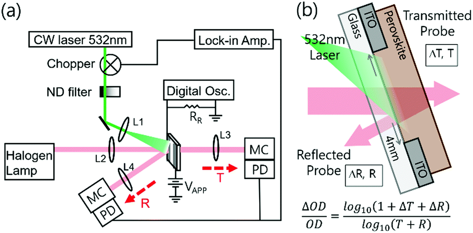 | ||
| Fig. 1 Schematic illustration of experimental setup and sample structure. (a) Photo-induced transmission and reflection spectroscopy (PITR) with quasi-steady-state photo-conductivity measurement setup. (b) Sample structure used in this study. Using one sample with this architecture, we measure both PITR and photo-conductivity, with and without external bias, respectively. | ||
To demonstrate the technique, we prepare polycrystalline MAPbI3 perovskite films using an acetonitrile-based solvent protocol32 (later referred to as MA-ACN). We spin-coated MAPbI3 films (∼400 nm) on top of a glass substrate with pre-patterned in-plane indium-tin oxide (ITO) electrodes. This MA-ACN technique leads to ultra-smooth films, minimizing optical scattering effects, resulting in predominantly specular reflection and transmission. We outline additional information on the device preparation in the experimental section. By using this setup together with the in-plane electrode device architecture, which we show in Fig. 1b, we can simultaneously perform optical and electrical measurements to gather transmittance (T), reflectance (R), photo-induced changes of transmittance (ΔT/T), reflectance (ΔR/R) and σPhoto data, in a single experiment.
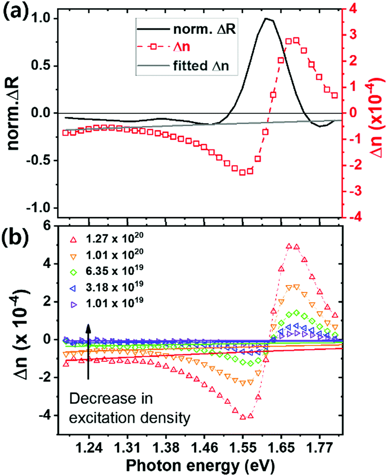
In Fig. 2a, we plot –ΔOD/OD to compare the shape of spectra together with the ΔT/T and ΔR/R. We observe the photobleaching peak at the band edge (around 1.63 eV) in both transmission and reflection.18,33 This strong change in absorption near the bandgap originates from band filling34 and bandgap renormalization.18 However, since our measurement is quasi-steady-state, where most photoexcited charge carriers will have thermalized, we expect band filling to dominate, resulting in the bleaching we observe near the band edge. We note that the peak of the ΔOD/OD spectra, is at lower energies than the peak of the ΔT/T and ΔR/R spectra. This is simply due to the shape of the OD spectrum, changing in an opposite fashion across the band edge, in comparison to the T and R spectra. This shifts the ΔOD/OD peak to lower energies, since OD is the denominator in this function. We illustrate this in Fig. S1 (ESI†).
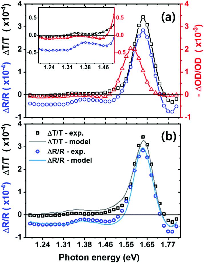 | ||
| Fig. 2 Photo-induced transmission and reflection spectra from experiment and fitting. (a) Photo-induced changes in transmission (black squares) and reflection (blue circles) with the calculated optical density change (red triangles, in negative sign for comparison) on the right axis as a function of incident photon energy (excitation density 1.01 × 1020 cm−1 s−1). The inset shows the spectra below the bandgap. (b) Measured photo-induced changes in transmission (black squares) and reflection (blue circles) plotted alongside simulated data (black and blue solid lines, correspondingly) using an optical transfer matrix model using Maclaurin's formula for the Kramers–Kronig transform. | ||
From Fig. 2a, we see that the transmission change in the sub-bandgap region, below 1.4 eV in particular, is small but slightly positive (bleaching). However, we do note that in some previous measurements this has been significant, and most likely erroneously interpreted as a bleaching due the filling of sub-bandgap trap states.35 Significantly, we observe a more negative ΔR/R signal in this region, consistent with reduced reflectance. Combining these spectra, we determine a small sub-bandgap increase in optical density (ΔOD/OD signal).
To explain these transmission and reflection changes, we model and extract the change in complex refractive index Δn(λ) + iΔk(λ). We use the transfer matrix model approach, together with the Kramers–Kronig relationship.36,37 We let the initial complex refractive index of perovskite be n0(λ) + ik0(λ). Upon photo-excitation, the refractive index changes to n1(λ) + ik1(λ). To find n1(λ) + ik1(λ), we searched through the space of possible solutions until we found the n′(λ) + ik′(λ) that, when fed into an optical transfer matrix model, best reproduces the measured R1 and T1. We chose the trial solutions to be Kramers–Kronig consistent, using a numerical implementation of Maclaurin's formula for the Kramers–Kronig transform.37 The obtained n′(λ) + ik′(λ) is equal to n1(λ) + ik1(λ), within the bounds of fitting error. It is then straightforward to calculate Δn(λ) + iΔk(λ) = n1(λ) + ik1(λ) − n0(λ) − ik0(λ). We take the initial complex refractive index n0(λ) + ik0(λ) from measurements in the literature.38 Indeed, we employ global fitting for the full range of each spectrum instead of a specific sub-range (e.g. sub-bandgap) for better reliability. In Fig. 2b we show both the experimental and fitted spectra, exhibiting close agreement throughout the entire spectrum. To generate different free carrier densities in the material, we illuminate at varying laser excitation densities, and conduct the fitting process to extract Δn using the same protocol.
Determining the charge carrier density and long-range mobility
We show the reflectance change of the perovskite after excitation in Fig. 3a. We also show on the same graph, our determined change in refractive index, Δn. The refractive index shows large variations near the band edge. Moreover, a negative change appears below the bandgap, which at low photon energy, increases with reducing photon energy.27 The carrier induced change in refractive index are related to changes of absorption through Kramers–Kronig relations, and can be explained by two effects in this charge density range: band filling and free carrier absorption.27 Firstly, after photo-excitation, the bottom of the conduction band minimum (CBM) will be filled by electrons that were excited from the valence band maximum (VBM). Consequently, the minimum energy required to excite an electron across the bandgap is increased giving rise to a widening of the bandgap.34 This band filling effect results in the strong feature we observe near the band edge. Secondly, free charge carriers can absorb an incident photon and be excited to a higher intraband energy state, which is known as the plasma effect.27,28,39 This increased free carrier intraband absorption following photo-excitation, results in a corresponding change in the real part of the complex refractive index, which is well described by the Drude model.27,40 Considering these phenomena, our results are consistent with what is observed in other direct bandgap semiconductors, such as GaAs,27 where Δn shows large changes near the bandgap energy, Eg, due to the band filling effect, and approaches zero at photon energies 0.1 to 0.2 eV above or below Eg. At energies far below the bandgap, the change in refractive index becomes increasingly negative, as a consequence of the increased free carrier density. We expect the refractive index to change with wavelength (λ) and free electron (N) and hole (P) densities, following,27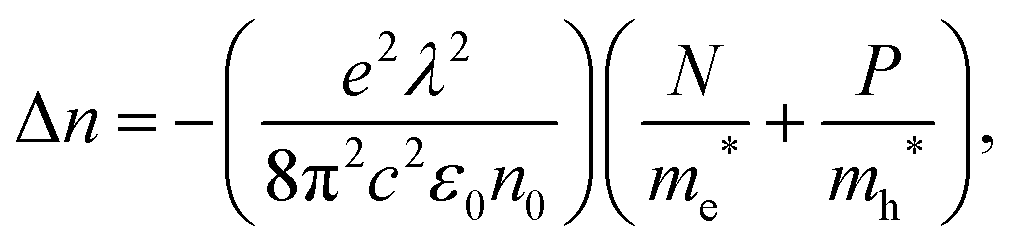 | (3) |
 | ||
| Fig. 3 Photo-induced change in refractive index and fitting for charge carrier density. (a) Light induced reflection change obtained from experiment, and refractive index change calculated from optical modeling. (b) Excitation density (photons cm−3 s−1) dependent light induced refractive index change (open symbols, dashed line is only to guide the eyes) and fitted data (solid lines) by eqn (3). | ||
At energies far enough below the bandgap, the contribution of the band filling effect to Δn are negligible. Therefore we fit the lower energy section of the Δn spectrum, between 1.2 and 1.3 eV, to eqn (3), and show such a fit as a light grey line in Fig. 3a. Within this energy range, we assume that the contribution to Δn from the band filling is negligible, hence Δn is predominantly related to the free carrier density. For our fitting we have used equal values of effective masses for electrons and holes from literature (me* = mh* = 0.208 me),41 and assumed equal number densities for free electrons and holes.42,43 To investigate the relationship between refractive index and free carrier density, we repeated the same measurement (Fig. S2, ESI†) and fitting described above, over a range of excitation densities.
With knowledge of the photo-induced charge carrier density, it is possible to determine the average mobility of electrons and holes, which we simply term μ, if the change in σPhoto is also known, following the relationship (1). We note that the average mobility, μ, which we present here, is half the value of the sum of electron and hole mobilities, Σμ, usually used for microwave and THz mobility estimations. Therefore, we measure the PITR and σPhoto sequentially using the same excitation density and laser illumination for the same device, as we illustrate in the schematic of Fig. 1b. For PITR we probe the region between the electrodes, and for σPhoto, we apply an external bias voltage to the electrodes. The resistance of the perovskite film, reduces under photo-excitation. Therefore, we measure the σPhoto by monitoring the voltage drop through a small resistor, which is in series with the in-plane conductivity device, following relationship,14,44,45
 | (4) |
We deem that our system is under quasi-steady-state conditions during most of the pulse period (70 Hz, 7 ms), i.e. the charge carrier generation and recombination rates are equal, as we elaborate upon in Fig. S3a (ESI†). We note that the measured σPhoto value is obtained after 3 min illumination (when an equilibrium is reached) to minimize the time dependent photo-doping effect (as shown in Fig. S3b, ESI†).43 We plot the σPhoto of the MA-ACN films as a function of excitation density in Fig. 4a. We show the mobility in Fig. 4b, which we determine to be in the range of between 0.47 to 2.2 cm2 V−1 s−1, over the excitation range which we study. We note that this mobility is lower than that determined through non-contact THz and microwave conductivity measurements, where values of the sum of electron and hole mobilities (μe + μh) are typically determined to be in the range of 20 to 40 cm2 V−1 s−1 (μe ∼ 10 to 20 cm2 V−1 s−1). The THz and microwave derived mobility is considered to probe short-range transport for metal halide perovskites, and is hence representative of the highest mobility within a crystalline domain, but is likely to neglect longer range scattering and trapping at grain boundaries and defects within the perovskite film.12,13,19,20,22,46,47 This difference might stem from the fact that we determined the lateral mobility using a 4 mm distance between the in-plane electrodes. Therefore, our results here include the effect of charge transport dynamics both within grains and across grain boundaries.46
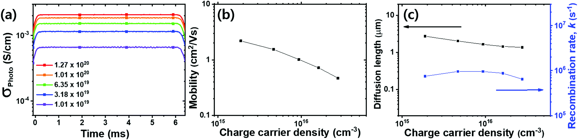 | ||
| Fig. 4 Evaluation of photo-induced optoelectronic properties of MAPbI3. (a) Excitation density (photons cm−3 s−1) dependent σPhoto of an MA-ACN polycrystalline film with in-plane electrodes, (b) charge carrier mobility (average between electron and hole) calculated using σPhoto and charge density determined by the Δn (c) charge carrier diffusion length and pseudo-first order recombination (k) rate calculated from the mobility and charge density. | ||
Under quasi-steady-state conditions, even though generation and recombination of charge carriers are continuously cycled, the free carrier density is constant (e.g. dN/dt = 0), implying that the recombination rate is equivalent to the generation rate G. Moreover, in the low charge carrier density regime, the recombination follows a pseudo-first order rate (k),12,13,22 and therefore we can write the quasi-steady-state conditions as G ∼ kN. Thus, knowing G and N, we can estimate an average carrier lifetime τ ∼ 1/k and corresponding pseudo-first order rate, which we show in Fig. 4c.
We can now evaluate the charge carrier diffusion length (LD) from our experimentally determined charge carrier mobility (μ) and carrier lifetime (τ) using the following equation:
 | (5) |
Comparison of the long-range charge carrier mobility within different perovskite films prepared via different deposition methodologies
The long-range mobility that we have estimated above is for MAPbI3 films processed from the acetonitrile/methylamine mixed solvent system. However, there are many other processing routes and perovskite compositions used in the research community. Here, we assess if the long-range charge carrier mobility of the perovskite layer is strongly influenced by the thin film processing methodology. To investigate this, and to assess the applicability of our technique to a broader set of materials, we prepared perovskite films using different fabrication processes, which are representative of state of the art perovskite absorbers used in the research community; CH3NH3PbI3 films from thermal co-evaporation (termed MA-evap),48 Cs0.17FA0.83Pb(I0.9Br0.1)3 (termed, FACs),2,49 and Cs0.05(FA0.83MA0.17)0.95Pb(I0.9Br0.1)3 (termed FAMACs)2,49,50 (see experimental section for the respective deposition procedures).In Fig. S4 (ESI†) we observe a significant difference in the σPhoto signal as a function of excitation density, with the FACs sample showing higher σPhoto than the FAMACs, with the MA-evap sample showing the lowest σPhoto. Knowing that the σPhoto is determined by the product of mobility and charge carrier density, increased σPhoto could be due to either higher carrier density (longer lifetime), or a higher charge carrier mobility, or a combination of the two. Therefore, in order to determine the charge carrier density for these three different samples, we performed the PITR measurement simultaneously to the σPhoto measurements, and plot the Δn of the three perovskite films as a function of total excitation density in Fig. S5 (ESI†). We show charge carrier mobility of the three different samples (in addition to the MA-ACN film) as a function of charge carrier density in Fig. 5.
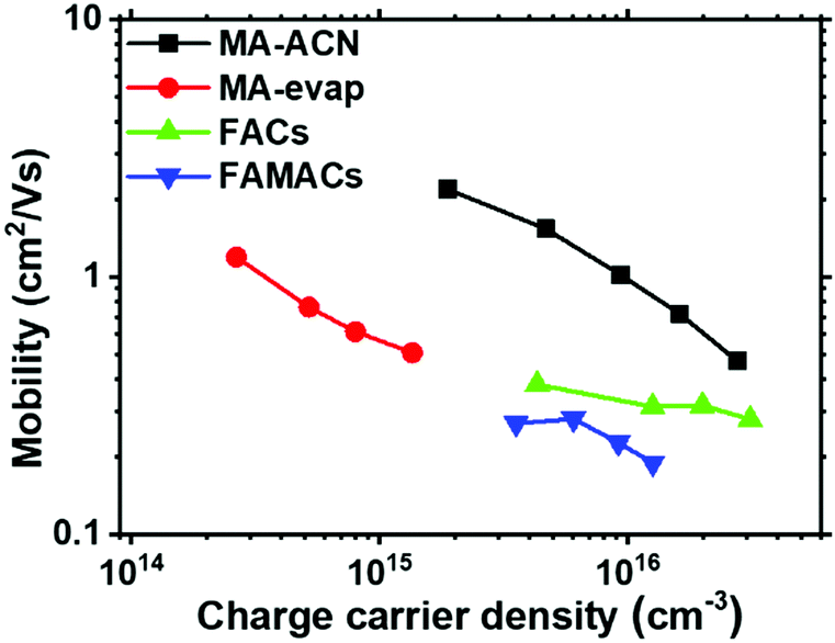 | ||
| Fig. 5 Long-range lateral mobility (average electron and hole mobility) with different composition of perovskites obtained by PITR; MA-ACN (MAPbI3 ACN solution processed), MA-evap (MAPbI3 co-evaporation processed), FACs (Cs0.17FA0.83Pb(I0.9Br0.1)3 solution processed), FAMACs (Cs0.05(FA0.83MA0.17)0.95Pb(I0.9Br0.1)3 solution processed). | ||
All films exhibit a lower peak mobility as compared to the MA-ACN film, and surprisingly, the evaporated film, which has relatively small grains, exhibits a higher charge carrier mobility, in comparison to the FACs and FAMACs films. Notably however, due to much faster recombination rate (Fig. S6, ESI†) in the evaporated MAPbI3 films, the steady-state charge carrier density is much lower than all the other films we studied. Our estimated mobility of all three perovskites is now in the range of between 1.19 to 0.51, 0.38 to 0.28 and 0.28 to 0.19 cm2 V−1 s−1 for MA-evap, FACs and FAMACs, respectively. We believe that these now represent good estimation of the long-range mobility within these perovskite films, and should therefore correlate with the relevant mobility for understanding optoelectronic devices where long-range transport occurs. This also implies that significant improvements should be possible in the present state-of-the-art perovskite solar absorbers, if we now focus efforts upon understanding parameters which can be tuned to improve this long-range mobility.
From our data, we observe that our highest mobilities (MA-ACN) are at the lower end, to an order of magnitude lower, than those estimated from early-time optical pump THz probe spectroscopy. This difference may be because here we determine the long-range mobility, which includes conduction between multiple crystalline grains, and fully influenced by the film surfaces.46,47 Furthermore, we do observe around one order of magnitude difference in mobility between our samples prepared in different ways. This may be due to differences in properties such as perovskite composition, grain sizes,1,32,51 trapping/detrapping processes, grain-boundary scattering,52 charging at grain boundaries, crystallinity and crystal orientation. In Fig. S7 (ESI†) we show SEM images of the different samples we have studied here for comparison.
Conclusions
In conclusion, we have presented a new method for determining the long-range lateral charge carrier mobility within perovskite films by quasi-steady-state optoelectronic techniques. By modeling the photo-induced sub-bandgap changes in the complex refractive index, obtained via photo-induced transmission and reflection (PITR) measurements, we determine the charge carrier density and combine it with the quasi-steady-state photo-conductivity. We evaluate the long-range lateral mobility of MAPbI3, Cs0.17FA0.83Pb(I0.9Br0.1)3, Cs0.05(FA0.83MA0.17)0.95Pb(I0.9Br0.1)3 as a function of free carrier density, and determine mobilities ranging from 2.2 down to 0.2 cm2 V−1 s−1 depending upon the preparation route and charge carrier density. Despite many years of intense research, to the best of our knowledge, our results represent the first accurate evaluation of the long-range lateral mobility in lead tri-halide perovskite films, and also highlight key advantages of quasi-steady-state method performed under similar excitation densities to a working solar cell. We believe that our technique will help to bring us closer to a complete understanding of long-range charge transport in different metal halide perovskite compounds, and other semiconductors, and gives us a new handle with which to examine and improve perovskite semiconductors.Author contributions
J. L. designed and performed all experiments and analyzed the data. M. T. H. and S. M. performed the optical simulations. N. S. conducted SEM measurements. N. S., N. K. N. and Y. H. L. fabricated solution processed perovskite films. J. B. P. and M. B. J. provided ultra-smooth co-evaporated perovskite films. J. M. B. and D. P. M. contributed with discussion and feedback for conductivity measurement. B. W. contributed to the spectroscopic data analysis. J. L. and H. J. S. wrote the manuscript. All authors discussed the results and reviewed the manuscript. B. W. and H. J. S. guided and supervised the overall project.Conflicts of interest
There are no conflicts to declare.Acknowledgements
This project was funded by EPSRC, Engineering and Physical Sciences Research Council grants, EP/M005143/1 and EP/P006329/1. B. W. acknowledges funding from the European Commission via a Marie-Skłodowska-Curie individual fellowship (REA Grant Number 706552-APPEL).Notes and references
- M. M. Lee, J. Teuscher, T. Miyasaka, T. N. Murakami and H. J. Snaith, Science, 2012, 338, 643–647 CrossRef CAS PubMed.
- D. P. McMeekin, G. Sadoughi, W. Rehman, G. E. Eperon, M. Saliba, M. T. Hörantner, A. Haghighirad, N. Sakai, L. Korte, B. Rech, M. B. Johnston, L. M. Herz and H. J. Snaith, Science, 2016, 351, 151–155 CrossRef CAS PubMed.
- H. S. Kim, C. R. Lee, J. H. Im, K. B. Lee, T. Moehl, A. Marchioro, S. J. Moon, R. Humphry-Baker, J. H. Yum, J. E. Moser, M. Grätzel and N. G. Park, Sci. Rep., 2012, 2, 591 CrossRef PubMed.
- A. N. Jumabekov, E. Della Gaspera, Z.-Q. Xu, A. S. R. Chesman, J. van Embden, S. A. Bonke, Q. Bao, D. Vak and U. Bach, J. Mater. Chem. C, 2016, 4, 3125–3130 RSC.
- S. D. Stranks, G. E. Eperon, G. Grancini, C. Menelaou, M. J. P. Alcocer, T. Leijtens, L. M. Herz, A. Petrozza and H. J. Snaith, Science, 2013, 342, 341–344 CrossRef CAS PubMed.
- D. W. DeQuilettes, S. Jariwala, S. Burke, M. E. Ziffer, J. T. W. Wang, H. J. Snaith and D. S. Ginger, ACS Nano, 2017, 11, 11488–11496 CrossRef CAS PubMed.
- C. Wehrenfennig, G. E. Eperon, M. B. Johnston, H. J. Snaith and L. M. Herz, Adv. Mater., 2014, 26, 1584–1589 CrossRef CAS PubMed.
- X. Y. Chin, D. Cortecchia, J. Yin, A. Bruno and C. Soci, Nat. Commun., 2015, 6, 1–9 Search PubMed.
- S. P. Senanayak, B. Yang, T. H. Thomas, N. Giesbrecht, W. Huang, E. Gann, B. Nair, K. Goedel, S. Guha, X. Moya, C. R. McNeill, P. Docampo, A. Sadhanala, R. H. Friend and H. Sirringhaus, Sci. Adv., 2017, 3, e1601935 CrossRef PubMed.
- G. W. P. Adhyaksa, E. Johlin and E. C. Garnett, Nano Lett., 2017, 17, 5206–5212 CrossRef CAS PubMed.
- J. M. Richter, F. Branchi, F. Valduga De Almeida Camargo, B. Zhao, R. H. Friend, G. Cerullo and F. Deschler, Nat. Commun., 2017, 8, 1–7 CrossRef CAS PubMed.
- M. B. Johnston and L. M. Herz, Acc. Chem. Res., 2016, 49, 146–154 CrossRef CAS PubMed.
- R. L. Milot, G. E. Eperon, H. J. Snaith, M. B. Johnston and L. M. Herz, Adv. Funct. Mater., 2015, 25, 6218–6227 CrossRef CAS.
- T. Leijtens, S. D. Stranks, G. E. Eperon, R. Lindblad, E. M. J. Johansson, I. J. McPherson, H. Rensmo, J. M. Ball, M. M. Lee and H. J. Snaith, ACS Nano, 2014, 8, 7147–7155 CrossRef CAS PubMed.
- K. C. Wang, J. Y. Jeng, P. S. Shen, Y. C. Chang, E. W. G. Diau, C. H. Tsai, T. Y. Chao, H. C. Hsu, P. Y. Lin, P. Chen, T. F. Guo and T. C. Wen, Sci. Rep., 2014, 4, 4756 CrossRef PubMed.
- D. S. Ginger and N. C. Greenham, Phys. Rev. B: Condens. Matter Mater. Phys., 1999, 59, 10622–10629 CrossRef CAS.
- D. Shi, V. Adinolfi, R. Comin, M. Yuan, E. Alarousu, A. Buin, Y. Chen, S. Hoogland, A. Rothenberger, K. Katsiev, Y. Losovyj, X. Zhang, P. A. Dowben, O. F. Mohammed, E. H. Sargent and O. M. Bakr, Science, 2015, 347, 519–522 CrossRef CAS PubMed.
- M. B. Price, J. Butkus, T. C. Jellicoe, A. Sadhanala, A. Briane, J. E. Halpert, K. Broch, J. M. Hodgkiss, R. H. Friend and F. Deschler, Nat. Commun., 2015, 6, 8420 CrossRef CAS PubMed.
- H. Oga, A. Saeki, Y. Ogomi, S. Hayase and S. Seki, J. Am. Chem. Soc., 2014, 136, 13818–13825 CrossRef CAS PubMed.
- J. G. Labram, N. R. Venkatesan, C. J. Takacs, H. A. Evans, E. E. Perry, F. Wudl and M. L. Chabinyc, J. Mater. Chem. C, 2017, 5, 5930–5938 RSC.
- P. Tiwana, P. Parkinson, M. B. Johnston, H. J. Snaith and L. M. Herz, J. Phys. Chem. C, 2010, 114, 1365–1371 CrossRef CAS.
- C. Wehrenfennig, M. Liu, H. J. Snaith, M. B. Johnston and L. M. Herz, Energy Environ. Sci., 2014, 7, 2269–2275 RSC.
- D. W. DeQuilettes, W. Zhang, V. M. Burlakov, D. J. Graham, T. Leijtens, A. Osherov, V. Bulović, H. J. Snaith, D. S. Ginger and S. D. Stranks, Nat. Commun., 2016, 7, 11683 CrossRef CAS PubMed.
- M. Abulikemu, S. Ould-Chikh, X. Miao, E. Alarousu, B. Murali, G. O. Ngongang Ndjawa, J. Barbé, A. El Labban, A. Amassian and S. Del Gobbo, J. Mater. Chem. A, 2016, 4, 12504–12515 RSC.
- T. Leijtens, E. T. Hoke, G. Grancini, D. J. Slotcavage, G. E. Eperon, J. M. Ball, M. De Bastiani, A. R. Bowring, N. Martino, K. Wojciechowski, M. D. McGehee, H. J. Snaith and A. Petrozza, Adv. Energy Mater., 2015, 5, 1–11 Search PubMed.
- Y. Takahashi, H. Hasegawa, Y. Takahashi and T. Inabe, J. Solid State Chem., 2013, 205, 39–43 CrossRef CAS.
- B. R. Bennett, R. A. Soref and J. A. Del Alamo, IEEE J. Quantum Electron., 1990, 26, 113–122 CrossRef CAS.
- T. M. Brenner, D. A. Egger, L. Kronik, G. Hodes and D. Cahen, Nat. Rev. Mater., 2016, 1, 15007 CrossRef CAS.
- O. Flender, J. R. Klein, T. Lenzer and K. Oum, Phys. Chem. Chem. Phys., 2015, 17, 19238–19246 RSC.
- T. A. Ford, PhD thesis, University of Cambridge, Department of Physics, 2006.
- S. Tassan and M. Ferrari, Limnol. Oceanogr., 1995, 40, 1358–1368 CrossRef.
- N. K. Noel, S. N. Habisreutinger, B. Wenger, M. T. Klug, M. T. Hörantner, M. B. Johnston, R. J. Nicholas, D. T. Moore and H. J. Snaith, Energy Environ. Sci., 2017, 10, 145–152 RSC.
- G. Grancini, A. R. Srimath Kandada, J. M. Frost, A. J. Barker, M. De Bastiani, M. Gandini, S. Marras, G. Lanzani, A. Walsh and A. Petrozza, Nat. Photonics, 2015, 9, 695–701 CrossRef CAS.
- J. S. Manser and P. V. Kamat, Nat. Photonics, 2014, 8, 737–743 CrossRef CAS.
- A. Abate, M. Saliba, D. J. Hollman, S. D. Stranks, K. Wojciechowski, R. Avolio, G. Grancini, A. Petrozza and H. J. Snaith, Nano Lett., 2014, 14, 3247–3254 CrossRef CAS PubMed.
- M. E. Ziffer, J. C. Mohammed and D. S. Ginger, ACS Photonics, 2016, 3, 1060–1068 CrossRef CAS.
- K. Ohta and H. Ishida, Appl. Spectrosc., 1988, 42, 952–957 CrossRef CAS.
- Q. Lin, A. Armin, R. C. R. Nagiri, P. L. Burn and P. Meredith, Nat. Photonics, 2015, 9, 106–112 CrossRef CAS.
- T. Ivanovska, C. Dionigi, E. Mosconi, F. De Angelis, F. Liscio, V. Morandi and G. Ruani, J. Phys. Chem. Lett., 2017, 8, 3081–3086 CrossRef CAS PubMed.
- C. H. Henry, R. A. Logan and K. A. Bertness, J. Appl. Phys., 1981, 52, 4457–4461 CrossRef CAS.
- A. Miyata, A. Mitioglu, P. Plochocka, O. Portugall, J. T. W. Wang, S. D. Stranks, H. J. Snaith and R. J. Nicholas, Nat. Phys., 2015, 11, 582–587 Search PubMed.
- Y. Yang, J. Gu, J. L. Young, E. M. Miller, J. A. Turner, N. R. Neale and M. C. Beard, Science, 2015, 350, 1061–1065 CrossRef CAS.
- K. Sveinbjörnsson, K. Aitola, X. Zhang, M. Pazoki, A. Hagfeldt, G. Boschloo and E. M. J. Johansson, J. Phys. Chem. Lett., 2015, 6, 4259–4264 CrossRef.
- A. Petrozza, C. Groves and H. J. Snaith, J. Am. Chem. Soc., 2008, 130, 12912–12920 CrossRef CAS PubMed.
- T. Leijtens, J. Lim, J. Teuscher, T. Park and H. J. Snaith, Adv. Mater., 2013, 25, 3227–3233 CrossRef CAS.
- A. A. Paraecattil, J. De Jonghe-Risse, V. Pranculis, J. Teuscher and J. E. Moser, J. Phys. Chem. C, 2016, 120, 19595–19602 CrossRef CAS.
- T. W. Crothers, R. L. Milot, J. B. Patel, E. S. Parrott, J. Schlipf, P. Müller-Buschbaum, M. B. Johnston and L. M. Herz, Nano Lett., 2017, 17, 5782–5789 CrossRef CAS PubMed.
- J. B. Patel, J. Wong-Leung, S. Van Reenen, N. Sakai, J. T. W. Wang, E. S. Parrott, M. Liu, H. J. Snaith, L. M. Herz and M. B. Johnston, Adv. Electron. Mater., 2017, 3, 1–6 Search PubMed.
- Z. Wang, Q. Lin, B. Wenger, M. G. Christoforo, Y. H. Lin, M. T. Klug, M. B. Johnston, L. M. Herz and H. J. Snaith, Nat. Energy, 2018, 3, 855–861 CrossRef CAS.
- M. Saliba, T. Matsui, J. Y. Seo, K. Domanski, J. P. Correa-Baena, M. K. Nazeeruddin, S. M. Zakeeruddin, W. Tress, A. Abate, A. Hagfeldt and M. Grätzel, Energy Environ. Sci., 2016, 9, 1989–1997 RSC.
- W. Zhang, S. Pathak, N. Sakai, T. Stergiopoulos, P. K. Nayak, N. K. Noel, A. A. Haghighirad, V. M. Burlakov, D. W. Dequilettes, A. Sadhanala, W. Li, L. Wang, D. S. Ginger, R. H. Friend and H. J. Snaith, Nat. Commun., 2015, 6, 10030 CrossRef CAS.
- J. Steinhauser, S. Faÿ, N. Oliveira, E. Vallat-Sauvain and C. Ballif, Appl. Phys. Lett., 2007, 90, 1–4 CrossRef.
Footnote |
| † Electronic supplementary information (ESI) available: Details of experiments, Table S1, Fig S1–S7. See DOI: 10.1039/c8ee03395a |
| This journal is © The Royal Society of Chemistry 2019 |