
Bifacial stamping for high efficiency perovskite solar cells†
Yong
Zhang‡
a,
Seul-Gi
Kim‡
a,
Donghwa
Lee
 b,
Hyunjung
Shin
c and
Nam-Gyu
Park
*a
b,
Hyunjung
Shin
c and
Nam-Gyu
Park
*a
aSchool of Chemical Engineering, Sungkyunkwan University, Suwon 440-746, Korea. E-mail: npark@skku.edu
bDepartment of Materials Science and Engineering, and Division of Advanced Materials Science, Pohang University of Science and Technology (POSTECH), Pohang 37673, Korea
cDepartment of Energy Science, Sungkyunkwan University, Suwon 440-746, Korea
First published on 17th November 2018
Abstract
We report a novel approach for a fast phase transition of FAPbI3 (FA = formamidinium) at low-temperature and the effective removal of interfacial recombination in MAPbI3 (MA = methylammonium). This method also allows for printing (patterning) of the perovskite on a desired area. The pre-annealed MAPbI3 and δ-phase FAPbI3 films were prepared by spin-coating DMSO and a polar aprotic solvent admixed precursor solution at 65 °C and 100 °C for about 1 min, respectively, to form adduct films containing DMSO. Two films were sandwiched without pressure by a method called bifacial stamping, and annealed at 100 °C for 9 min, which resulted in complete δ → α phase transition of FAPbI3 and led to a power conversion efficiency (PCE) of 18.34%. The stamped MAPbI3 demonstrated a PCE of 20.18% that was much higher than the conventionally annealed MAPbI3 (∼17.4%) mainly due to a much higher fill factor and open-circuit voltage. Optical and structural studies revealed that DMSO-mediated ion exchange plays a vital role in the phase transition of FAPbI3 and the surface modification of MAPbI3. Theoretical calculation results further support the role of DMSO in the phase transition at low temperature. Stamping was applied to EAPbI3 (EA = ethylammonium), where photoinactive yellow EAPbI3 changed to photoactive EAPbI3 with a PCE of 13.02% after stamping with MAPbI3. The DMSO-mediated EA/MA ion exchange reaction during the stamping process created a new layer having a gradient solid solution of EAPbI3 and MAPbI3, which was responsible for the abnormally high PCE of the EAPbI3 based perovskite solar cell. Facilitated ion transport by a Lewis base (such as DMSO) reservoir in the perovskite adduct film is suggested to be involved in the bifacial stamping procedure.
Broader contextLead halide-based perovskite materials and devices have attracted tremendous attention from the scientific community in the last six years since the report on a solid-state perovskite solar cell in 2012. High quality perovskite film fabricating methodologies could play a crucial role toward obtaining high performance photovoltaic properties. In this work, we report for the first time a bifacial stamping method for high efficiency perovskite solar cells. This method allows us to obtain high quality MAPbI3 (MA = methylammonium) films with enhanced photovoltaic properties, a fast delta-to-alpha phase transition of FAPbI3 (FA = formamidinium) at low temperature and a transformation of EAPbI3 (EA = ethylammonium) from a non-photovoltaic material to a photoactive material. Moreover, the perovskite area can be patterned by the bifacial stamping procedure, leading to new printed photovoltaics. We propose that the bifacial stamping method is a protocol for not only improving photovoltaic performance but also for phase transition and compositional micro-tuning by means of facilitated ion transport in the residual DMSO present in the pre-annealed perovskite film. |
Introduction
Lead halide based perovskites have recently emerged as prominent materials for efficient and low-cost solar technology. The recent urgent research activity into perovskite solar cells (PSCs) has been triggered by the solid-state perovskite solar cells with power conversion efficiencies (PCE) of 9.7% and 500 h-stability without encapsulation,1 following two subtle but very important perovskite-sensitized solar cells.2,3 Reports on unusual properties of perovskites, including high absorption coefficients,4 long charge-carrier diffusion lengths,5,6 small exciton binding energies,7 low trap densities8 and facile fabrication,9 gave insights into the superb photovoltaic performances of PSCs. As a result of a better understanding of the optoelectronic properties of perovskites, a PCE exceeding 22%10 was achieved using compositional engineering. Recently, a record PCE of 23.3% was certified,11 which surpasses the PCEs of current high efficiency thin film solar cells.The most commonly used perovskite photovoltaic materials for PSCs are MAPbI3 (MA = methylammonium) and FAPbI3 (FA = formamidinium). MAPbI3 became the primary perovskite material used for perovskite solar cells because of its suitable bandgap energy of ca. 1.6 eV, and its solution processable and low-temperature (∼100 °C) fabrication procedure.2,12–14 However, grain boundaries and defects formed during solution processing act as trap-states for charge recombination, which can deteriorate the photovoltaic performance.15 Compared to MAPbI3, FAPbI3 is expected to be better in photovoltaic performance because of its narrower bandgap of ca. 1.4–1.5 eV,16–18 higher thermal stability19,20 and stronger p-type characteristics.21 However, since polymorphic FAPbI3 has two structural phases of a photoactive black α phase and a photoinactive yellow δ non-perovskite phase,17,22 relatively long annealing at high temperature (∼150 °C) is required to undergo a phase transition from the δ to the α phase. Such long annealing conditions may induce degradation of the FAPbI3 film.22,23 Phase transition from δ phase to α phase FAPbI3 at a lower temperature of about 100 °C was suggested by replacing a certain amount of FA+ with cesium ions (Cs+) and/or MA+, however, this required the incorporation of the relevant Br− anions simultaneously, leading to an increase in the bandgap.20,24,25 Recently, the δ → α phase transformation of FAPbI3 was reported using dimethyl sulfoxide (DMSO) solvent-vapor annealing at 100 °C.26 Although exceptional grain growth with micrometer-sized α-FAPbI3 was obtained, its photovoltaic performance was not investigated.
Since most spin-coated perovskite films are likely to contain solvents, removal of the residual solvent in the film is important in terms of efficiency and stability. Solid–solid or solid–vapor reactions are expected to be promising methods to minimize the residual solvent. Co-evaporation of reactants in a vacuum is a typical solid–solid reaction, where MAI and PbCl2 were co-evaporated to form a ca. 15% efficient MAPbI3 film.27 However, in the evaporation method, it is somewhat difficult to control the stoichiometry and the thickness of the perovskite film despite the versatile solvent-free fabrication process.28 Another method is a sequential (two-step) deposition method, where the solid PbI2 is reacted with MAI.29 MAI can be treated in the solution form or the vapor type (quasi vacuum reaction). A reaction mechanism for a two-step spin-coating using a MAI solution was reported to explain the crystallization and changes in grain size of MAPbI3.30–32 A two-step method was also applied to form a high quality α-FAPbI3 film, where an intermolecular exchange method was developed to replace the DMSO in the PbI2–DMSO adduct.22 In terms of methodologies for high efficiency PSCs, no attempt has been made using a so-called bifacial stamping method that results in a layer-to-layer interaction between a MAPbI3 film and a FAPbI3 film or an EAPbI3 (EA = ethylammonium) film. While we were preparing the manuscript, a similar method was reported but the two MAPbI3 films were sandwiched and pressed.33 According to the Goldschmidt tolerance factor (t = (RA + RI)/√2(RPb + RI)) in APbI3,34,35 formability of a perovskite can be expected when t ranges from 0.8 to 1. It is hard to form an EAPbI3 perovskite phase because of the calculated tolerance factor of t = 1.05.36 Although EAPbI3 was determined to be a pseudo 2H perovskite-like structure,37 the EA cation is considered to be suitable for the perovskite structure according to the revised tolerance factor including the globularity factor.38
Here, we report for the first time a bifacial stamping method for high efficiency perovskite solar cells. This method allows us to fabricate high efficiency PCSs based on not only MAPbI3 but also other compositions such as FAPbI3 or EAPbI3. Non-pressed bifacial contact can lead to morphologically high quality MAPbI3 with a defectless interface and fast δ → α phase transformation of FAPbI3 at low temperature. For the MAPbI3 case, the bifacial stamping method leads to a PCE of about 20% that is much higher compared to that of material made using a conventional spin-coating technique showing an average PCE of about 17%. The bifacially stamped FAPbI3 exhibits a PCE of over 18% that is also higher than that of material made using the conventional spin-coating method. Moreover, we have discovered that a 548 nm-thick EAPbI3 film contacted with a MAPbI3 film results in a PCE of over 13%. Structural and opto-electronic studies were performed to elucidate the substantial improvements obtained after the bifacial stamping method.
Results and discussion
Stamping method
Fig. 1(a) and (b) display a schematic representation of the bifacial stamping process. This process involves pre-annealing and stamping steps. As can be seen in Fig. 1(a), MAPbI3, FAPbI3 and EAPbI3 films were separately prepared, where the FAPbI3 or EAPbI3 film was prepared by a spin-coating method and heated at 100 °C for around 1.5 min, whereas, the MAPbI3 film was prepared by an adduct method10 and pre-annealed at 65 °C for 1 min. In the second step (Fig. 1(b)), which is called “bifacial stamping”, the 65 °C-pre-annealed MAPbI3 (hereafter referred to MAPbI3-before) film was simply laid on the 100 °C-annealed FAPbI3 or EAPbI3 (hereafter referred to FAPbI3-before or EAPbI3-before) film, which was followed by annealing at 100 °C for 9 min without pressure. After the stamping process, the films were detached. The stamped films were called MAPbI3(F or E)-after, FAPbI3(M)-after and EAPbI3(M)-after, where MAPbI3 (F)-after means that the MAPbI3 film was stamped with FAPbI3 and FAPbI3(M)-after means that FAPbI3 was stamped with MAPbI3. Yellow FAPbI3 and EAPbI3 films turned black after the bifacial stamping process (Fig. 1(c) and (e)). MAPbI3 (F)-after shows a deep brown color but the color of the central part looks grayish brown (Fig. S1, ESI†). More interestingly, in the FAPbI3-after and EAPbI3-after films, only the parts contacted with MAPbI3 show a dark brown color but the uncontacted areas are still yellowish, which indicates that the band gaps of FAPbI3 and EAPbI3 contacted with MAPbI3 are reduced. By using this phenomenon, a patterned α and δ phase FAPbI3, where the dark red “SKKU” contains α phase and the masked area has yellow δ phase, was printed by inserting a mask between the MAPbI3 and the FAPbI3 (Fig. 1(c) and Fig. S2, ESI†). UV-vis transmittance in Fig. 1(d) shows that the yellow part in the patterned FAPbI3 film has a higher transmittance in the wavelength range from 400 to 800 nm due to a wider band gap, whereas most visible light is absorbed by the red colored part due to the reduced band gap and the formation of the α phase. The highly transparent yellow δ-FAPbI3 has potential for photovoltaic window applications. The stamped α phase FAPbI3 (FAPbI3(M)-after) with the “SKKU” letters still shows a dark brown color even after aging for 8 months in ambient conditions, while the MAPbI3(F)-after film turns yellow (Fig. S3, ESI†), indicating that the stamped FAPbI3 shows much higher material stability. A portrait was printed by the stamping method using a mask inserted in between the MAPbI3 and the EAPbI3 (Fig. 1(e)), where the red color results from direct contact of the EAPbI3 with the MAPbI3 and the yellow color is maintained because EAPbI3-before is uncontacted with MAPbI3. UV-vis transmittance spectra show that transmittance below 800 nm for the red EAPbI3-after part is lower than that for the yellow part (Fig. 1(f)), which confirms that the optical band gap of the EAPbI3 is changed after stamping contact. This bifacial stamping method can also be applied to a large area of 10 cm × 10 cm size. As can be seen in Fig. S4 (ESI†), the large-area stamped films show similar results as observed in those of the smaller size of 2.4 cm × 2.4 cm in Fig. S1 (ESI†). It should be noted that in the large scale bifacial stamping method the stamped perovskite film quality was found to depend on the pre-annealed film quality.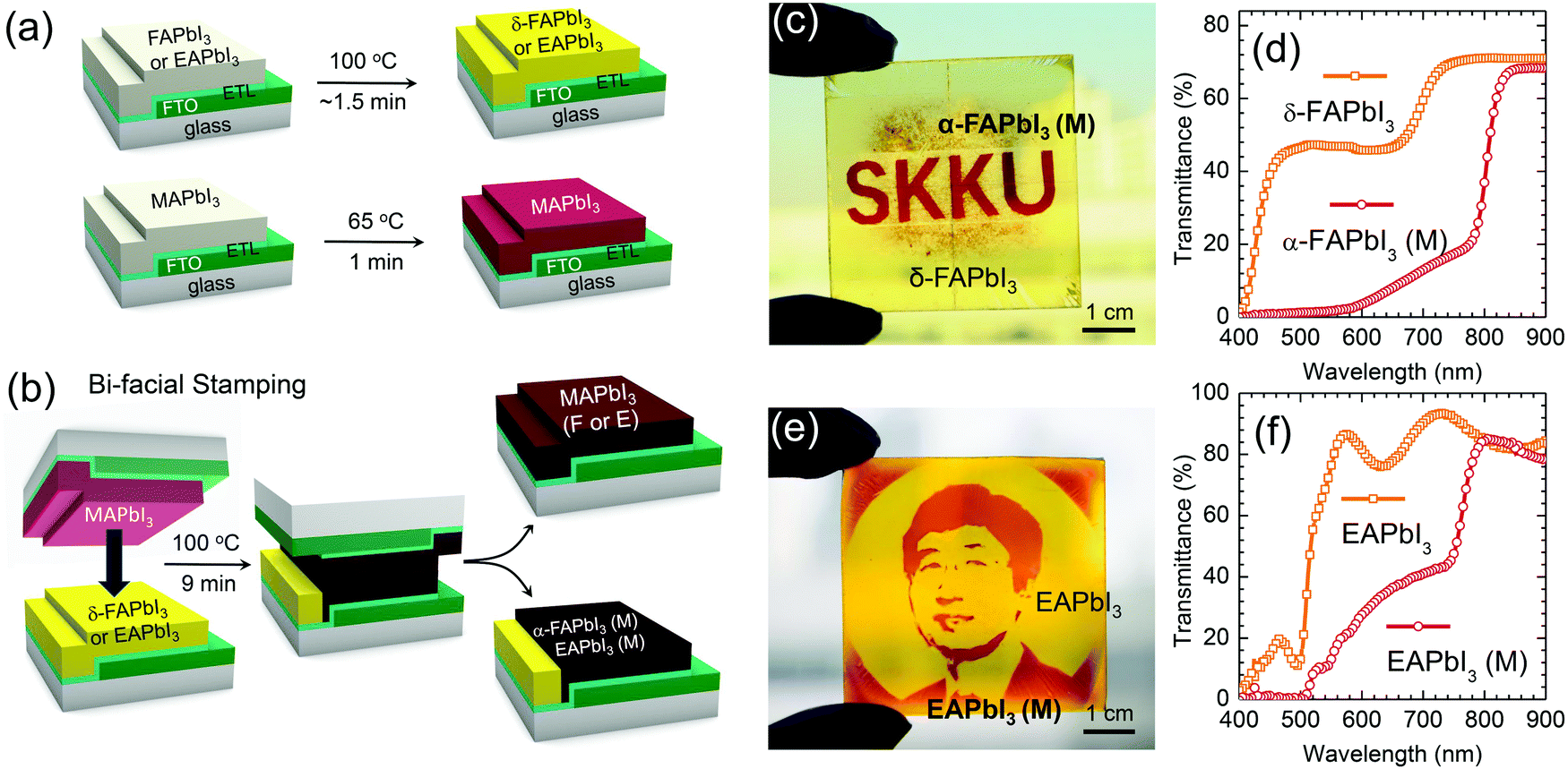 | ||
| Fig. 1 Schematic illustration of the stamping method comprising two steps of (a) pre-annealing and (b) the bifacial stamping procedure, where each perovskite film was prepared at low temperature with a short annealing time in the pre-annealing step and two perovskite films were bifacially contacted at 100 °C for 9 min without pressure in the stamping step. (b) Perovskite printing technology based on the bifacial stamping process, where (c) “SKKU” letters were printed by inserting a mask between the MAPbI3 and the yellow δ-FAPbI3 due to the δ → α phase transition of FAPbI3 and (d) the corresponding transmittance spectra. (e) A portrait image using an EAPbI3 film was produced by inserting a mask between the MAPbI3 and the yellow EAPbI3 due to the reduction of the band gap and (f) the corresponding transmittance spectra. | ||
Structure evolution
We studied the structures of the MAPbI3, FAPbI3 and EAPbI3 before and after the stamping process using X-ray diffraction (XRD). In Fig. 2(a), the pre-annealed MAPbI3 (MAPbI3-before) shows the typical tetragonal phase, where small XRD peaks at low angles (6.55°, 7.21° and 9.17°) are attributed to the MAI–PbI2–DMSO intermediate phase.12,13,39 The intensity ratio of the 9.17° peak to the (110) peak at 14.1° increases from 0.07 (MAPbI3-before) to 0.49 (MAPbI3(F)-after) after the stamping process, which indicates that the MAI–PbI2–DMSO intermediate phase is more enhanced. For the FAPbI3 before and after contacting with MAPbI3, the pre-annealed FAPbI3 (FAPbI3-before) exhibits a typical δ phase with a sharp (010) plane at 11.8° and (021) plane at 26.2° (Fig. 2(b)), corresponding to the hexagonal P63mc space group.21,40 It was reported that the δ → α phase transformation in pure FAPbI3 requires a temperature over 125 °C.21,40 However, after stamping with the MAPbI3 film, the (010) peak disappeared but new peaks at 13.9° and 28.1° appeared that correspond to (−111) and (−222) planes for the trigonal FAPbI3 perovskite phase (P3m1).40,41 For the EAPbI3 case, EAPbI3-before was determined to be of a non-perovskite phase (orthorhombic, Pmmn group), which was consistent with our previous results published elsewhere.37 However, after stamping with MAPbI3, peaks for the EAPbI3 orthorhombic phase disappeared, while strong peaks appeared at 13.94° and 26.49°, which are at the same position as those of the (110) and (220) peaks observed for MAPbI3(E)-after, along with unknown peaks (Fig. 2(c)). This indicates that EAPbI3(M)-after consisted of a solid solution of MAPbI3 and an EA/MA mixed cation phase. MAPbI3 after stamping with EAPbI3 showed a typical XRD pattern corresponding to tetragonal MAPbI3. It was found that the (110), (224) and (314) peak positions observed at around 14.1°, 40.62° and 43.14°, respectively, for MAPbI3-before and -reference, were shift to lower angles of 14.05°, 40.41° and 43.09° for MAPbI3(F)-after and 13.97°, 40.22° and 42.75° for MAPbI3(E)-after (Fig. 2(d)), which is indicative of expansion of the lattice constant after the stamping process. Lattice expansion underlines that a certain amount of MA is likely to have been replaced by the larger cations of FA or EA. To understand the XRD peak shift of MAPbI3 after stamping with FAPbI3, XRD patterns of MAPbI3 prepared under different conditions were compared (Fig. S5, ESI†). MAI–PbI2–DMSO powder, as-coated MAPbI3 film (without annealing), MAPbI3(glass)-after (stamping of the MAPbI3-before film with bare glass without FAPbI3), MAPbI3(F)-after and MAPbI3(F)-after-with-further-annealing (additional annealing of MAPbI3(F)-after for 10 min at 100 °C) were prepared. A strong peak at around 14°, corresponding to the (110) plane of tetragonal MAPbI3, was observed for all of the samples, which is indicative of the presence of a perovskite phase. At low angles of 2 theta ranging from 6° to 10°, three peaks were detected for the MAI–PbI2–DMSO powder, while no peaks appeared for the as-coated MAPbI3 film, which indicates that the residual DMSO in the as-coated MAPbI3 film was not likely to be strongly coordinated with the perovskite lattice. Thus, the three distinct peaks at low angles observed for the MAPbI3(F)-after implies strong coordination of DMSO with the perovskite lattice. To understand the basis for the strong interaction of DMSO with MAPbI3 in the MAPbI3(F)-after, a pre-annealed MAPbI3 film (MAPbI3-before) was stamped with bare glass. It is interesting to see that the low angle peaks were observed but their intensities were almost negligible. In addition, the 2 theta values of the (224) and (314) peaks were higher for the MAPbI3(glass)-after film than for the MAPbI3(F)-after film. The low angle peaks were not detected after further annealing of the MAPbI3(F)-after, which was due to evaporation of DMSO after further annealing. Thus, the peak shift along with the enhanced low angle peaks observed in the MAPbI3(F)-after were due to the probable incorporation of FA ions and the strong coordination of the perovskite lattice with the residual DMSO. For the FAPbI3 side, from the detailed analysis of the peak position, the (−333) peak for FAPbI3(M)-after was found to shift to a higher degree compared to the reference α-FAPbI3 (Fig. 2(e)), which underlines a decrease in lattice constant that is probably due to the diffusion of smaller MA+ into the FAPbI3 during the bifacial stamping process. The selected area electron diffraction pattern inset in Fig. 2(f) clearly matches with the trigonal structure, known as the α phase of FAPbI3 in FAPbI3(M)-after. With the zone axis of [0001], the diffracted spots were indexed as {020}, {220}, and {240}. Interplanar spacings of (420) and (020) were around 0.24 and 0.40 nm, respectively, as shown in the high resolution lattice image (Fig. 2(f)). Upon stamping, the δ phase of FAPbI3 is indeed transformed to α phase FAPbI3 as confirmed by HRTEM analysis. | ||
| Fig. 2 X-ray diffraction (XRD) patterns of (a) MAPbI3 films, (b) FAPbI3 films and (c) EAPbI3 films before and after stamping, along with MAPbI3 and FAPbI3 reference films and the calculated powder XRD pattern of tetragonal MAPbI3 (space group I4/mcm, a = 8.800 Å, c = 12.685 Å) and trigonal FAPbI3 (α-phase, P3m1 space group, a = 8.981 Å, c = 11.006 Å). The MAPbI3 reference was obtained from annealing an as-coated MAPbI3 film at 65 °C for 1 min and 100 °C for 9 min based on a conventional spin-coating process. The α-FAPbI3 reference film was obtained by annealing an as-coated FAPbI3 film at 150 °C for 40 min based on a conventional spin-coating process. Detailed XRD patterns for (d) MAPbI3 and (e) FAPbI3 before and after stamping. (f) TEM image of FAPbI3 after stamping with MAPbI3. The inset is a selected area electron diffraction (SAED) pattern. | ||
To further understand the phase transition of FAPbI3 after stamping with MAPbI3 under such mild conditions, several experiments were carried out. As shown in Fig. S6(a) and (b) (ESI†), phase transitions of FAPbI3 were observed by contacting the pre-annealed δ-FAPbI3 film with the MAPbBr3–DMSO film and even with bare FTO. However, the surface of the resulting FAPbI3 was very rough and DMSO damaged the film to form many pin-holes. In other words, MA+ cations and DMSO were simultaneously required for the phase transition of the well-defined FAPbI3 film, which was confirmed by additional experiments showing no phase change of the FAPbI3 upon contacting it with MAPbI3 without DMSO (Fig. S6(c), ESI†). A polar aprotic solvent like DMF was found to play a similar role to DMSO in the phase transformation of FAPbI3, which was proved by contacting the pre-annealed FAPbI3 film (FAPbI3-before) with a non-annealed MAPbI3 film deposited using a precursor solution containing only DMF (Fig. S6(d), ESI†). Phase transition of FAPbI3 was even observed for the δ-FAPbI3 film pre-annealed for a longer time, probably with a lower DMSO content in the FAPbI3 film, which underlines that residual DMSO in the MAPbI3 film is essential for the δ → α phase transition of FAPbI3 (Fig. S6(e), ESI†). The co-existence of MA+ and DMSO (or DMF) in the MAPbI3 film before stamping is thus a prerequisite for the phase transformation, which indicates that solvent-driven MA+ ion migration into FAPbI3 is probably involved in the phase transformation. This was confirmed by an experiment where the addition of a small amount of MAI in the FAPbI3 precursor solution can easily change the color to black under annealing at 100 °C for 10 min (Fig. S6(f), ESI†). Thus solvent-driven cation exchange is a possible mechanism in the stamping process.
Morphology
Plane-view SEM images Fig. 3(a) and (b) show that the grain size of MAPbI3 was increased from ca. 170 nm before stamping to ca. 700 nm after stamping. The cross-sectional SEM images of the MAPbI3-before show a smooth film surface, enabling the δ-FAPbI3 film to contact well with the MAPbI3 film, which becomes a rough surface with a pyramidal shape after stamping. The grain size of MAPbI3 is also increased after stamping with EAPbI3 (Fig. 3(c)) but its surface is quite different from the surface after contacting with FAPbI3 observed in Fig. 3(b), which indicates that the film surface of MAPbI3 is influenced by the stamped materials. The grain size and morphology of FAPbI3 are altered by stamping as can be seen in Fig. 3(d) and (e), which is attributed to the δ → α phase transition.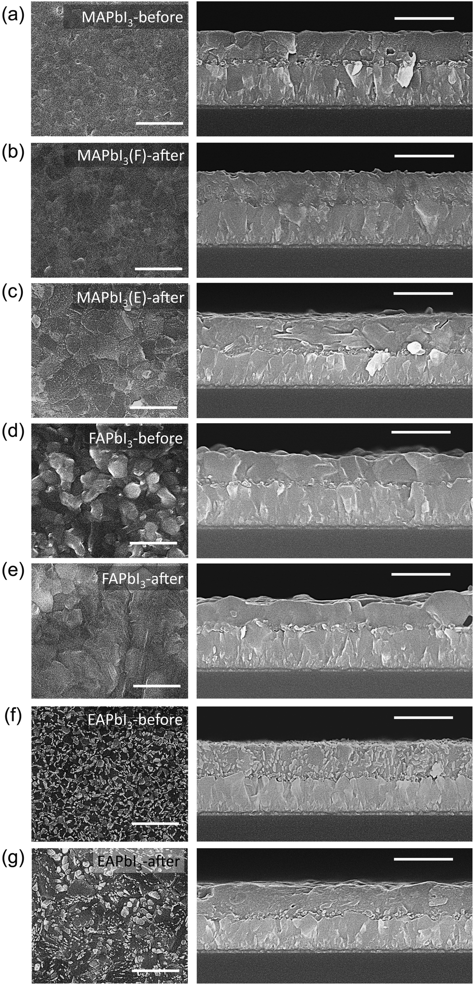 | ||
| Fig. 3 (left) Plane-view and (right) cross-sectional scanning electron microscopy (SEM) images of (a) MAPbI3-before, (b) MAPbI3(F)-after, (c) MAPbI3(E)-after, (d) FAPbI3-before, (e) FAPbI3(M)-after, (f) EAPbI3-before and (g) EAPbI3-after. The perovskite layers were fabricated on a glass/FTO/block layer-TiO2 (bl-TiO2)/mesoporous-TiO2 (mp-TiO2) substrate. Scale bars are 1 μm. | ||
There is big change in the morphology of EAPbI3 before and after stamping of the film, where small grains before stamping (Fig. 3(f)) are changed to bigger sizes with different morphologies (Fig. 3(g)). When considering the mechanism of the stamping method, DMSO-driven MA+ ion migration could happen and some of the EA cations could presumably be replaced by MA+ cations, leading to a solid solution of EAPbI3 and MAPbI3.
Optical properties
UV-vis absorption and photoluminescence (PL) were measured to investigate any change in optical properties after stamping. In Fig. 4(a), MAPbI3 shows enhanced absorption intensity together with a blue shift of the onset edge after stamping with FAPbI3. The optical bandgap determined by a Tauc plot (inset in Fig. 4(a)) was slightly reduced from 1.602 eV to 1.596 eV. In Fig. 4(b), the steady-state PL peak of MAPbI3 also shifts from 766 nm to 778 nm after stamping, which is consistent with the decrease in the bandgap. The PL intensity of the MAPbI3(F)-after film was 6-fold higher than that of the reference MAPbI3 film, which was mainly due to the surface passivation by DMSO.42 The red-shift in the PL peak in MAPbI3 after stamping is indicative of a partial incorporation of FA ions in the MA sites.43 The absorption coefficient of MAPbI3 in Fig. 4(c) was slightly increased after stamping, which was also consistent with the increased absorbance. Fig. 4(d) shows a change in the absorption onset wavelength from 440 nm to 840 nm, which is indicative of a change in bandgap due to the δ → α phase transformation. The optical bandgap was changed from 2.83 eV to 1.53 eV as determined from the Tauc plot in the inset of Fig. 4(d), showing clear evidence for the formation of the α phase after bifacial contact. However, it was noted that a large difference was observed in the PL intensity, as shown in Fig. 4(e), where the PL intensity at 787 nm of FAPbI3-before was significantly decreased after the stamping process and the peak position was slightly red-shifted to 807 nm. To investigate the basis for the abnormally high PL intensity for the FAPbI3-before film, additional experiments were conducted. We prepared two different FAPbI3 precursor solutions by dissolving FAI, PbI2 and DMSO in DMF or GBL. For the PL study (Fig. S7(a), ESI†) the δ-FAPbI3 films were deposited on bare glass using the DMF- or GBL-based precursor solutions. A strong PL peak was observed at 790 nm and its intensity was increased as the annealing temperature was increased from 25 °C to 100 °C for the δ-FAPbI3 films prepared from the DMF-based solution (Fig. S7(b), ESI†). In addition, another peak with negligible intensity was simultaneously observed at 486 nm but its intensity decreased with annealing temperature (Fig. S7(b), ESI†). A slight red-shift was also observed upon increasing the annealing temperature. For the δ-FAPbI3 films using the GBL-based precursor solution, a strong PL peak occurred only for the 100 °C-annealed FAPbI3, along with a low-wavelength peak with negligible intensity. Although XRD confirmed that the samples annealed at 100 °C were δ-phase FAPbI3 for both DMF- and GBL-cases, black dots were observed on the surface of the yellow film (Fig. S7(d), ESI†). Black dots, probably related to black α-FAPbI3, were homogeneously distributed on the yellow δ-FAPbI3 (Fig. S7(e), ESI†) and thus may not have been detected by XRD. The high intensity of the PL peak of the δ-FAPbI3 at around 790 nm was presumably attributed to the Förster Resonance Energy Transfer (FRET) between δ-FAPbI3 as a donor and α-FAPbI3 as an acceptor (Fig. S7(f), ESI†), where α-FAPbI3 absorbs the emission light of δ-FAPbI3 and emits fluorescence at around 790 nm.44,45 A significant enhancement of the absorption coefficient was observed after the stamping process due to black α-FAPbI3 formation (Fig. 4(f)).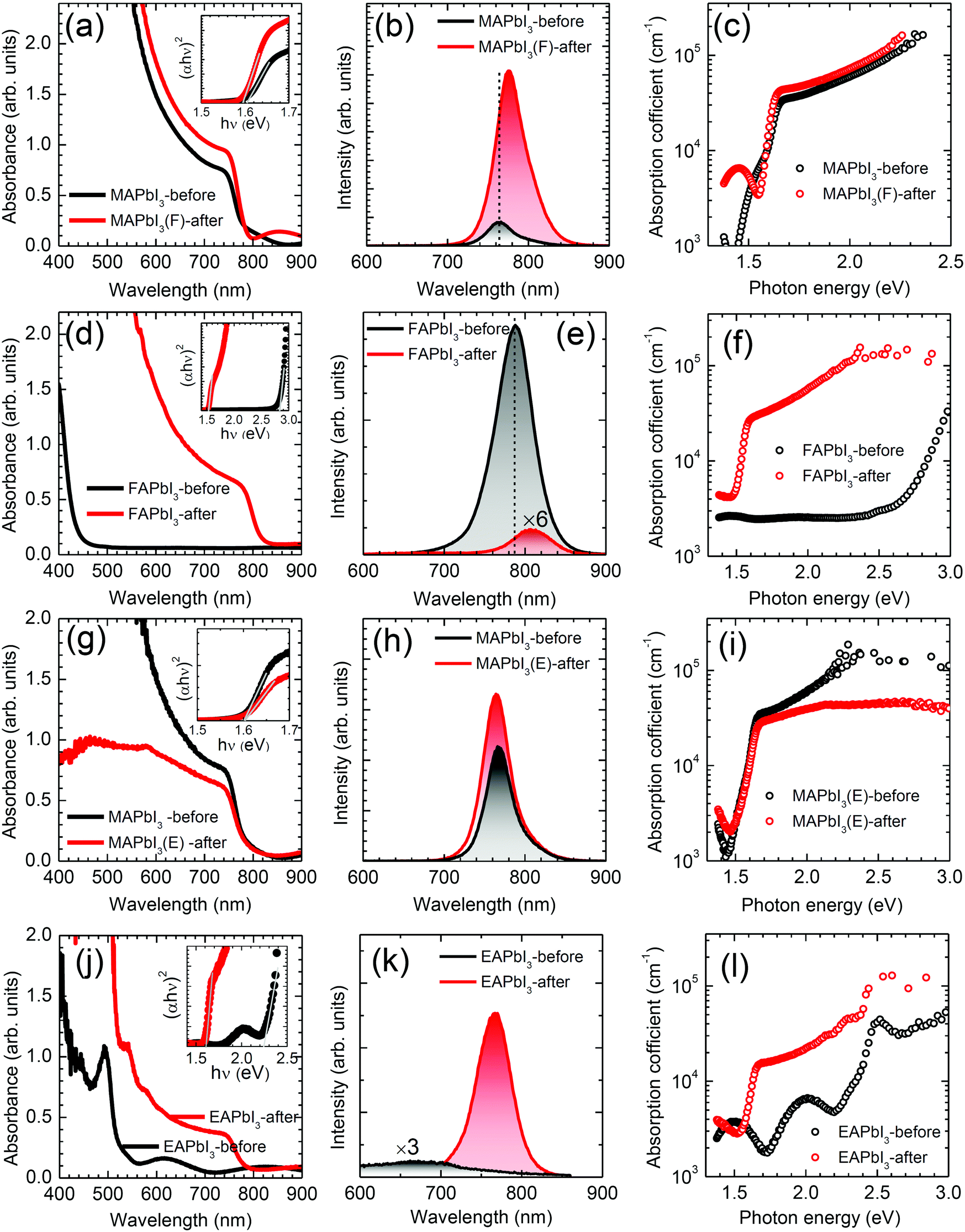 | ||
| Fig. 4 UV-vis absorbance, steady-state photoluminescence (PL) and absorption coefficient of (a–c) MAPbI3 before and after stamping with FAPbI3, (d–f) FAPbI3 before and after stamping with MAPbI3, (g–i) MAPbI3 before and after stamping with EAPbI3 and (j–l) EAPbI3 before and after stamping with MAPbI3. Insets in (a), (d), (g) and (j) are the Tauc plots obtained using the equation (αhv)2 = k(hν − Eg), where k is a constant, hν is the photon energy, α is the absorption coefficient, and Eg is the optical bandgap. The excitation wavelength for the PL measurements was 372 nm. The absorption coefficient was calculated using the equation α = ln[(1 − R)2/T]/d = 2.303A/d, where α is the absorption coefficient, R is the reflectance, T is the transmittance, A is the absorbance and d is the perovskite film thickness. The thickness was determined from the cross-sectional SEM images. The perovskite films were fabricated on bare glass. | ||
Fig. 4(g–i) show changes in the optical properties of MAPbI3 before and after stamping with EAPbI3. Contrary to stamping with FAPbI3, the absorbance of MAPbI3 is decreased after stamping with EAPbI3 (Fig. 4(g)). Moreover, the absorption coefficient is slightly decreased and the PL intensity is not substantially enhanced and is without notable peak shift (Fig. 4(h) and (i)). This indicates that cations in the counterpart of MAPbI3 play an important role in the optical properties of the MAPbI3 after stamping. For EAPbI3, the absorbance, PL intensity and absorption coefficient are significantly enhanced after stamping as shown in Fig. 4(j–l). Since the optical bandgap is decreased from 2.26 eV before stamping to 1.61 eV after stamping, the ethylammonium cations are considered to be largely exchanged with the methylammonium cations in EAPbI3.
Time-resolved PL (TRPL) decay profiles were studied to investigate the effect of stamping on the carrier life time. As shown in Fig. 5, the PL decay of the perovskite films on glass without ETL before stamping and after stamping were compared. The data are fit with a biexponential decay equation, which is listed in Table S1 (ESI†). The fast decay component is attributed to non-radiative recombination related to interface (or surface) defects, and the slow component is ascribed to radiative recombination related to bulk properties.8,46 In Fig. 5(a), the MAPbI3-before film shows biexponential decay resulting in an effective lifetime of 14.45 ns with a fast component of τ1 = 2.61 ns and a slow component of τ2 = 245.80 ns. After stamping, MAPbI3 exhibits a much prolonged effective lifetime of 308.42 ns due to a much longer τ2 = 537.34 ns. The enhanced lifetime is indicative of the suppression of trap-assisted recombination and an improvement of the quality of the bulk perovskite. On the other hand, the effective carrier lifetime of δ-FAPbI3 (FAPbI3-before) is 132.98 ns, which is much longer than 75.19 ns of α-FAPbI3 (FAPbI3-after), due to a large portion of fast decay components in spite of the longer τ2, which is probably due to FRET effects as mentioned previously. Stamping on FAPbI3 reduces the τ1 from 36.45 ns to 1.13 ns and increases the τ2 from 295.60 ns to 428.53 ns, which is indicative of a significant reduction of defects (Fig. 5(b)). MAPbI3, after stamping with EAPbI3, exhibits a slightly longer effective lifetime compared to MAPbI3 before stamping (Fig. 5(c)), which is consistent with the slight increase in steady-state PL intensity. Due to the negligible PL intensity in the EAPbI3 film before stamping as observed in Fig. 4(k), no detectable carriers were measured (Fig. 5(d)), while EAPbI3 after stamping shows carriers with lifetimes of τ1 = 11.40 ns and τ2 = 286.61 ns, enabling effective generation of carriers but with rather short-lived life times.
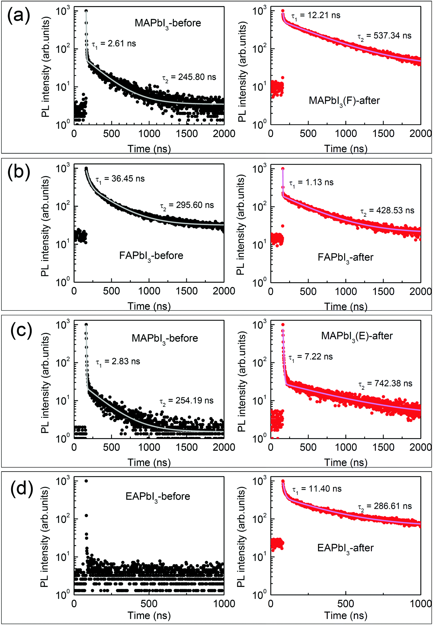 | ||
| Fig. 5 Time-resolved photoluminescence (TRPL) for (a) MAPbI3(F), (b) FAPbI3, (c) MAPbI3(E) and (d) EAPbI3 before (left) and after (right) stamping. For the TRPL measurements, the perovskite films were fabricated on a bare glass substrate. The excitation wavelength was 372 nm. | ||
Mechanism
We have speculated based on XRD, UV-vis and PL studies that there are two possible factors of cation exchange between MA+ and FA+ during stamping and residual DMSO in the MAPbI3-before film prepared at 65 °C for 1 min (60 s) that might be involved in the δ → α phase transition of FAPbI3 at an unusually low temperature of 100 °C and for a short annealing time of 9 min by the stamping process. In order to elucidate the hypothesis, the pre-annealing time at 65 °C was changed from 10 s to 600 s (10 min) because the content of residual DMSO in the MAPbI3-before film was expected to depend on the pre-annealing time. As can be seen in Fig. S8(a) (ESI†), the stamped MAPbI3 (MAPbI3(F)-after) and FAPbI3 (FAPbI3-after) films were strongly affected by the pre-annealing time. At a short pre-annealing time such as 10 s the stamped MAPbI3 film, obtained at 100 °C for 9 min, exhibited a mostly whitish surface along with a dark black color on the edge of the film, which gradually turned black as the pre-annealing time increased. The stamped FAPbI3 films showed complementary colors, where the film area with a mostly black surface formed by stamping with the short pre-annealed MAPbI3 film was gradually reduced with pre-annealing time. The whitish part of the MAPbI3-after film decreased sharply and disappears at 300 s, while the black part in the FAPbI3-after film remained at more than 80% for a pre-annealing time of 300 s (Fig. S8(b) and (c), ESI†). The test results indicated that the content of residual DMSO in the pre-annealed MAPbI3 plays a critical role in the δ → α phase transition of FAPbI3, where the phase transition is sufficiently induced by DMSO-rich but not by DMSO-poor conditions. In the DMSO-poor case, the difficulty in the phase transition was due to the fact that most of the residual DMSO was likely to be evaporated under the stamping conditions of 100 °C for 9 min. The content of residual DMSO in the pre-annealed MAPbI3 film is of importance for the phase transition of FAPbI3, however, the DMSO in the pre-annealed FAPbI3 film has hardly any influence on the stamping results (Fig. S6(e), ESI†). The effect of pre-annealing time on the photovoltaic performance was investigated. From the statistical photovoltaic parameters in Fig. S9 (ESI†), the stamped MAPbI3 films obtained from pre-annealing times shorter than 40 s resulted in larger deviations of all photovoltaic parameters and much lower mean values due to the deep whitish areas (Fig. S10(a), ESI†). Compared to the black part on the edge of the film, much lower J–V properties were observed from the deep whitish part (Fig. S10(b), ESI†). In the case of a short pre-annealing time such as 30 s, the DMSO-rich conditions led to a large grain size of MAPbI3 along with white needle-like structures at the grain boundary (Fig. S11(a), ESI†), which were likely to be responsible for the thick whitish rough surface and low photovoltaic performance.47 On the other hand, the black FAPbI3 area, as the counterpart to the whitish MAPbI3, showed featureless grains without a distinct grain boundary (Fig. S11(b), ESI†). For the stamping between MAPbI3 and EAPbI3, a similar trend was observed on the effect of pre-annealing time, although the color contrast was not as pronounced compared to the FAPbI3 case (Fig. S12, ESI†). Studies on the effect of pre-annealing time revealed that the DMSO-mediated interface reaction was critical in producing high quality perovskite films and controlling the content of residual DMSO in the pre-annealed MAPbI3 film is highly important for phase transformation and photovoltaic performance of MAPbI3 and its counterpart. The best pre-annealing conditions for stamping MAPbI3 with both FAPbI3 and EAPbI3 was found to be 60 s.To understand the reason why DMSO is strongly coordinated with the MAPbI3 lattice but not with FAPbI3 after stamping as observed in the XRD studies shown in Fig. 2, the electrostatic potential (EP) of DMSO was compared with those of the MA+, FA+ and EA+ cations because EP can give information on charge distribution of molecules and thereby the extent of the interactions between the DMSO and the cations. Fig. 6(a–d) show EP maps, where the red parts and the blue parts represent electron-rich and electron-deficient regions, respectively. The EP values are also listed in Table S2 (ESI†). For DMSO, a negative EP of −249.755 kJ mol−1 in DMF is concentrated around the oxygen atom in DMSO due to the strong electronegativity of oxygen, exhibiting an electron-rich red color, while the positive EP of 154.721 kJ mol−1 is distributed around the two methyl groups, showing an electron-deficient blue color in the EP map. Relatively large positive EP values were estimated for the cations, which is due to the positively charged cation properties. In MA+ and EA+ cations, the electron-rich parts were found to be the methyl groups since the positive charge is located on the nitrogen. On the other hand, for the FA+ case, electrons were localized on the nitrogen but electrons were relatively poor on the N–C–N due to the resonance structure. Interaction between the electron-rich part of DMSO (oxygen) and the electron-deficient part of the cations (nitrogen for MA+ and EA+ but N–C–N for FA+) is expected, which might be estimated from differences in the EP (ΔEP = EP(cation) − EP(DMSO)). Fig. 6(e) shows that ΔEP between DMSO and MA+ is relatively larger than that between DMSO and FA+, which allows us to expect a stronger interaction between DMSO and MA+ and thus this can explain the incorporation of DMSO in the stamped MAPbI3 film.
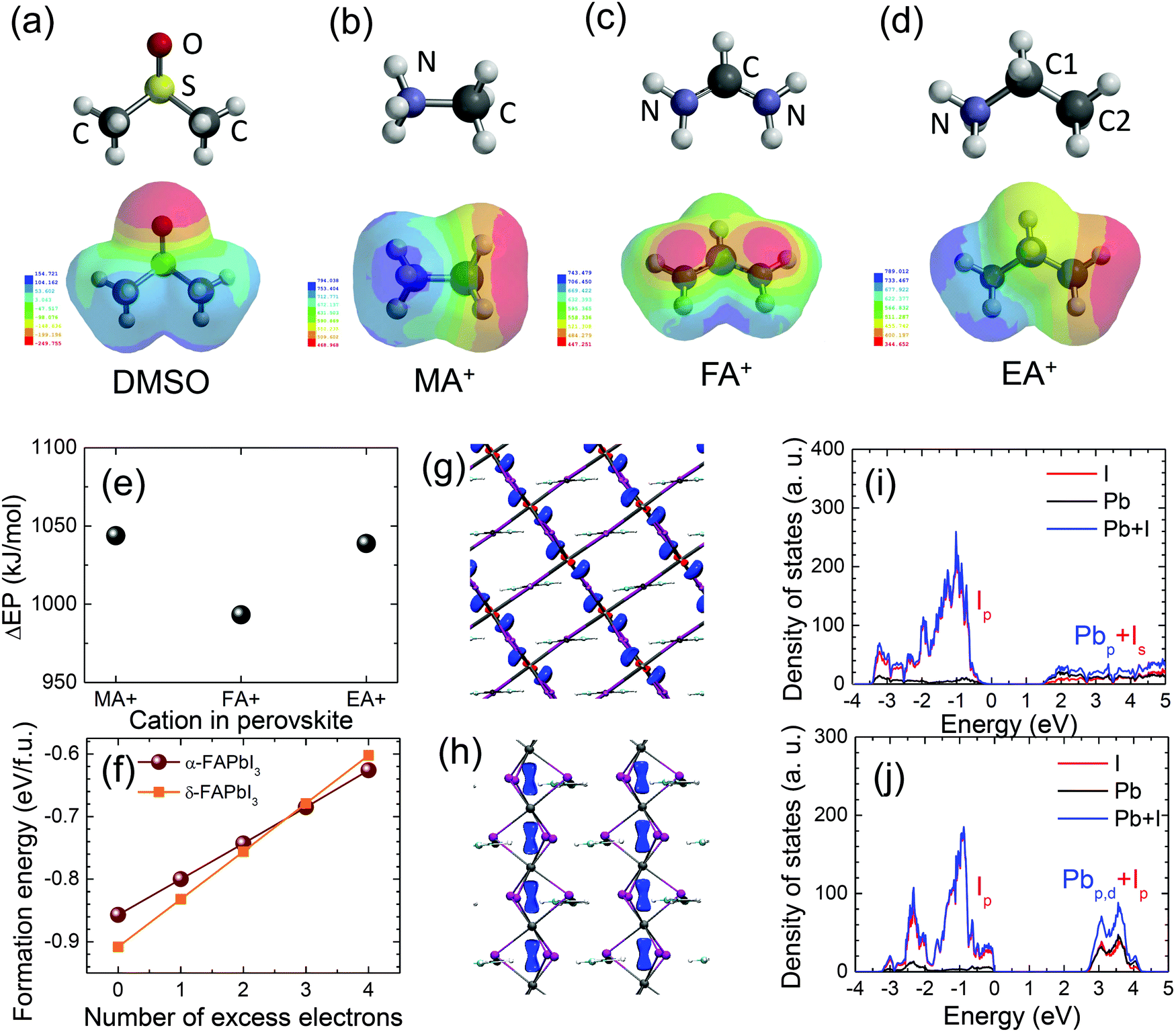 | ||
| Fig. 6 Electrostatic potential (EP) maps of (a) dimethyl sulfoxide (DMSO) (b) the methylammonium cation (MA+), (c) the formamidinium cation (FA+) and (d) the ethylammonium (EA+) cation (IsoValue = 0.002). Gray balls represent hydrogen. The red and blue colors in the EP map represent the electron-rich regions and the electron-deficient regions, respectively. (e) Differences in EP between DMSO and the cations (ΔEP = EP(cation, blue) − EP(DMSO, red)) in DMF. (f) Formation energies of α- and δ-FAPbI3 as a function of the number of excess electrons. (g and h) Spatial distribution of excess electrons and (i and j) partial density of states (PDOS) of Pb and I in (g and i) α-FAPbI3 and (h and j) δ-FAPbI3. Charge density is plotted at the level of 0.001e. | ||
We performed DFT calculations to understand the preferred formation of α-FAPbI3 during the stamping process. Since it is well known that DMSO is a strong electron donor, we look at the effect of excess electrons on the formation energy of α-FAPbI3 and δ-FAPbI3. We prepared a 3 × 3 × 2 supercell for α-FAPbI3 and a 3 × 3 × 3 supercell for δ-FAPbI3 in which both systems have an identical system size with 54 formula units (648 atoms and 2916 electrons). Fig. 6(f) shows the formation of α-FAPbI3 (blue) and δ-FAPbI3 (red) as a function of excess electrons (excess electrons can be created by the DMSO-rich conditions). At neutral state, the formation energy of δ-FAPbI3 was 0.051 eV lower than that of α-FAPbI3, indicating that the formation of δ-FAPbI3 is energetically preferred over α-FAPbI3. With the inclusion of excess electrons, however, the energy difference between the two phases decreases. Eventually, α-FAPbI3 is energetically preferred over δ-FAPbI3 with more than three excess electrons. The formation energy for α-FAPbI3 is 0.006 eV and 0.024 eV lower than those of δ-FAPbI3 with three and four excess electrons. (The electron concentrations associated with three and four excess electrons are 2.16 × 1020 cm−3 and 2.89 × 1020 cm−3.) Thus, excess electrons can expedite the formation of α-FAPbI3 over δ-FAPbI3. From the calculations, δ-FAPbI3 was expected to be stabilized without excess Lewis base DMSO. With the stamping of MAPbI3, the concentration of DMSO between the MAPbI3 and δ-FAPbI3 increased and δ-FAPbI3 was not stabilized due to the fact that the α-FAPbI3 formation energy was lower than that for δ-FAPbI3 when a certain amount of DMSO existed in the interface. So, the contacted area of δ-FAPbI3 can be transformed to the α-FAPbI3 phase under low temperature.
We further investigated the partial density of states (PDOS) and spatial distribution of an excess electron for both α-FAPbI3 and δ-FAPbI3 to understand the enhanced energetic stability of α-FAPbI3 under excess electrons (see Fig. 6(g–j)). As can be seen, the valence bands of both α- and δ-FAPbI3 are composed of the p orbital of iodine (I), while the conduction bands are made up of the hybridization between the p orbital of Pb and the s orbital of I for α-FAPbI3 and the hybridization between the p and d orbital of Pb and the p orbital of I for δ-FAPbI3. As a result, the excess electron tends to go into the hybridized state between the Pb and I ions. This can also be confirmed by the spatial distribution of an excess electron; the excess electron is mainly distributed between the Pb and I ions for both α- and δ-FAPbI3 as shown in the blue regions in Fig. 6(g) and (h). We now discuss why the formation of α-FAPbI3 is preferred with the existence of excess electrons, such as for the DMSO-rich case. The energetic preference for α-FAPbI3 under excess electrons can be understood by the differences in the bandgaps between the two phases; the bandgap of α-FAPbI3 (1.47 eV) is just half of the bandgap of δ-FAPbI3 (2.85 eV) (Fig. 6(i) and (j)). As a result, excess electrons in δ-FAPbI3 occupy relatively higher energy states than those of α-FAPbI3 and increase the energy of the system faster. Eventually, with more than three excess electrons, α-FAPbI3 can be energetically lower than δ-FAPbI3. Thus, α-FAPbI3, with the smaller bandgap, is preferentially formed by stamping with the electron donor DMSO-rich MAPbI3. In summary, our DFT calculations have shown that the preferential formation of α-FAPbI3 with DMSO is due to the differences in energy position of the conduction bands for excess electrons.
Photovoltaic properties
For the photovoltaic studies, TiO2 or SnO2 was used for the electron transport layer (ETL). First, we investigated the stamping effect using a MAPbI3 film deposited on a mp-TiO2/bl-TiO2 ETL. Full cell structures are shown by the cross-sectional SEM images (Fig. 7(a) and (b)), where the layer thickness after stamping is around 550 nm for MAPbI3 and 520 nm for FAPbI3. The photovoltaic performance of the stamped MAPbI3 was compared with that of the reference MAPbI3, directly annealed at 100 °C for 9 min, in Fig. 7(c). Photovoltaic parameters are listed in Table S3 (ESI†). The stamped MAPbI3 showed the best PCE of 19.36% at reverse scan with Jsc = 21.82 mA cm−2, Voc = 1.126 V and FF = 0.788, while the reference MAPbI3 showed a lower PCE of 17.43% with Jsc = 20.97 mA cm−2, Voc = 1.066 V and FF = 0.780. After stamping, all of the photovoltaic parameters of MAPbI3 were improved, which was probably due to the modification of the interface between the MAPbI3 and spiro-MeOTAD. The J–V hysteresis was not altered, even after the stamping process, which was attributed to the large capacitance at the TiO2 interface rather than the spiro-MeOTAD/perovskite interface.48–50 The device based on the stamped FAPbI3 showed almost comparable photovoltaic performance compared to the reference α-FAPbI3 annealed at 150 °C (Fig. 7(d)), where it was noted that the stamping process improved the FF from 0.705 to 0.766 due to modification of the surface of the FAPbI3 contacting the spiro-MeOTAD. Fig. 7(e) demonstrates stabilized current and PCE, where the PCE is confirmed to be higher for the MAPbI3(F)-after (PCE = 17.39% after 100 s) than for the reference MAPbI3 (PCE = 14.94% after 100 s). | ||
| Fig. 7 Cross-sectional SEM of complete solar cells and the corresponding J–V curves with the structure of glass/FTO/bl-TiO2/mp-TiO2/perovskite/spiro-MeOTAD/Ag based on (a and c) the MAPbI3(F)-after and (b and d) the FAPbI3-after. (e) Steady-state current density and PCE measured at maximum power voltage. J–V curves were measured at a scan rate of 0.13 V s−1 (voltage settling time of 200 ms) with reverse scan under AM 1.5 one sun illumination. | ||
A planar structure with a thin SnO2 layer as the ETL was applied to investigate the photovoltaic performance of the stamped perovskites. In Fig. 8, J–V curves are compared before and after stamping and the corresponding data are listed in Table S4 (ESI†). After stamping, all of the photovoltaic parameters were substantially improved. The stamped MAPbI3(F)-after showed a PCE of 20.18% (Jsc = 22.02 mA cm−2, Voc = 1.126 V, FF = 0.814) (Fig. 8(d)) that is much higher than the PCE of 9.73% before stamping (Fig. 8(a)). It should be noted that the improvement of the photovoltaic properties of MAPbI3 after the FAPbI3 stamping process is mainly due to the diffusion of FA+ into the MAPbI3 and interface modification. Since a MAI–PbI2–DMSO phase is formed after stamping (Fig. 2(a)), one can speculate that the MAI–PbI2–DMSO phase might be related to the improved photovoltaic performance. In order to investigate the effect of MAI–PbI2–DMSO, we checked the photovoltaic performance of the heat-treated MAPbI3(F)-after film by further annealing the stamped MAPbI3(F) film with the film-side up to eliminate MAI–PbI2–DMSO. The removal of MAI–PbI2–DMSO was confirmed by the XRD pattern shown in Fig. S5 (ESI†). The device based on the further annealed film still showed a high PCE of around 20% (Fig. S13, ESI†). This indicated that the improved photovoltaic performance of the MAPbI3(F)-after material is mainly due to diffusion of FA+ into the MAPbI3 along with the interface modification rather than the presence of a byproduct MAI–PbI2–DMSO phase due to the bifacial stamping method. For FAPbI3 in Fig. 8(b) and (e), negligible PCE is observed before stamping due to the presence of a non-perovskite yellow phase, while the stamped FAPbI3 demonstrates a PCE of 17.76% (Jsc = 21.84 mA cm−2, Voc = 1.062 V and FF = 0.766) along with negligible J–V hysteresis. EAPbI3 is not able to exhibit photovoltaic performance before stamping (Fig. 8(c)), whereas the EAPbI3 after stamping with MAPbI3 shows a PCE as high as 13.02% (Fig. 8(f)) with Jsc = 18.60 mA cm−2, Voc = 1.071 V and FF = 0.654. Inter-mixing of MA and EA after stamping and thereby the formation of a solid-solution of EAPbI3 and MAPbI3, as confirmed by the XRD in Fig. 2(c), is responsible for the high PCE of the stamped EAPbI3. We further investigated the underlying ion exchange during stamping between MAPbI3 and EAPbI3 using XRD. Fig. S14(a) (ESI†) shows that the XRD pattern of EAPbI3 was changed after stamping. The peak at 2 theta of 11.66° can be assigned to (004) for the EAPbI3 before stamping,37 which almost disappears and a new peak at 12.1° is observed after stamping. This new peak is also observed from the EA-rich EA0.8MA0.2PbI3, which however, cannot be found for MA-rich phases such as EA0.4MA0.6PbI3. For EA1−xMAxPbI3 with x ≥ 0.4, a peak is observed at 13.94°, which is attributed to the presence of the (110) plane of MAPbI3. Thus, a peak at 13.94° for the EAPbI3-after film corresponds to the (110) peak for MAPbI3-before, which indicates that the MAPbI3 phase was formed in the EAPbI3 layer after stamping. From the XRD study, pure EAPbI3 before stamping is likely to change to a mixed composition containing MAPbI3, with a solid solution of MAPbI3 and EAPbI3 and EAPbI3 (Fig. S14(b), ESI†). To further investigate whether the stamping process can lead to incorporation of MA+ cations into the EAPbI3, possibly via DMSO-mediated ion exchange, the optical properties were investigated. Fig. S15(a) (ESI†) shows that the film color gradually changed from yellow to dark reddish black as x increased (MA content increased) due to replacement of EA with MA. For x = 0, a pure EAPbI3 phase, a PL peak with almost negligible intensity was observed at 488 nm, attributed to the wide bandgap of EAPbI3, which was unusually increased as x increased to x = 0.3 (Fig. S15(b), ESI†). This indicates that non-radiative recombination might be reduced by the addition of MA+ cations. In the long wavelength region (Fig. S15(c), ESI†) a peak observed at 680 nm shifts to 760 nm along with an increase in intensity (Table S5, ESI†) as MA content increases, which is due the presence of MAPbI3 in the solid solution and/or a substitution effect. For the stamped EAPbI3, the strongest PL peak is observed at 760 nm along with no peak at ∼488 nm. When considering the PL measurements, a 372 nm laser was incident on the top film surface side, and a very strong PL at 760 nm without a peak at 488 nm was due to MAPbI3. This confirms our model suggested in Fig. S14(b) (ESI†). Since the stamped EAPbI3 film was composed of a mixed phase of MAPbI3, EA1−xMAxPbI3 and EAPbI3 (see Fig. S14, ESI†), it was interesting to investigate the photovoltaic performance of EA1−xMAxPbI3 depending on x. In Fig. S16 (ESI†), pure EAPbI3 shows a PCE as low as 0.23%. However, as the content of MA increased, the PCE increased from 2.23% to 6.81% and to 10.71% when x increased from 0.2 to 0.4 and to 0.6. The mixing ratio of 60% MA and 40% EA showed the best PCE. Nevertheless the PCE still has a gap to reach the PCE of stamped EAPbI3 (Fig. S16(h), ESI†). Besides, it is hard to include such a high concentration of MA in EAPbI3 by only a mild stamping process. The gradient structure of MAPbI3/EA1−xMAxPbI3/EAPbI3 might be responsible for the improvement of the photovoltaic performance. The photovoltaic performance based on the MAPbI3 stamped with EAPbI3 (MAPbI3(E)-after) was not as good as the performance of the MAPbI3(F)-after (see Table S4, ESI†). This might be attributed to a certain amount of EA that was incorporated in MAPbI3 after stamping. The hysteresis was much reduced for the SnO2-based MAPbI3 device (Fig. 8(d)) compared to the TiO2-based MAPbI3 one (Fig. 7(c)), but still existed. The trap density of the MAPbI3 was slightly reduced after stamping but was almost comparable to that of reference MAPbI3 as estimated from the trap-filled limited voltage (Fig. S17, ESI†), which was responsible for the hysteresis.23,51
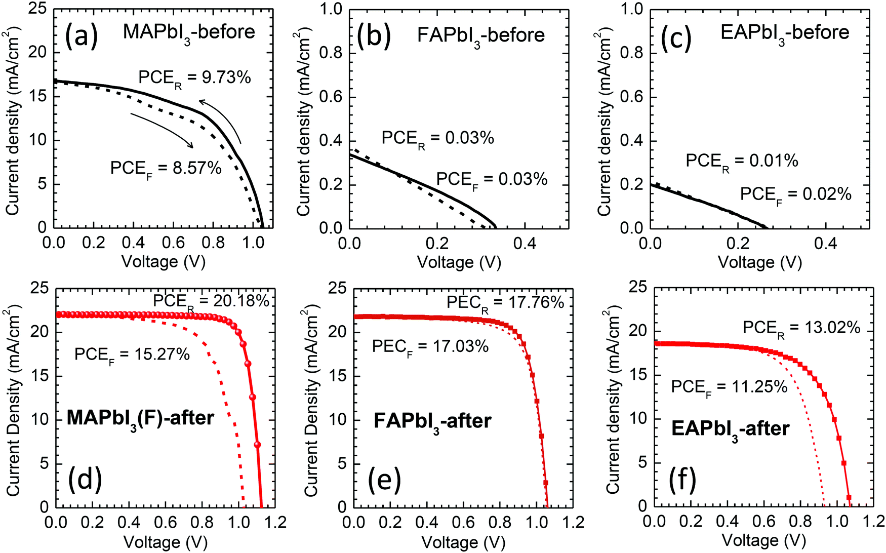 | ||
| Fig. 8 Reverse and forward scanned J–V curves of the best performing devices with (a and d) MAPbI3, (b and e) FAPbI3 and (c and f) EAPbI3 before and after stamping, measured at a scan rate of 0.13 V s−1 (voltage settling time of 200 ms) under AM 1.5 one sun illumination. PCEF and PCER represent the PCE values obtained from forward scanned and reverse scanned data respectively. | ||
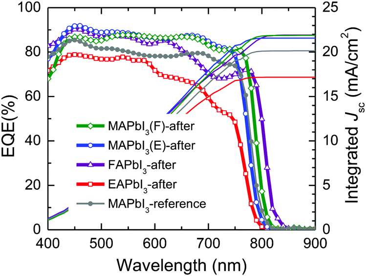
As shown in Fig. 9, the external quantum efficiency (EQE) was monitored for the devices with the stamped MAPbI3, FAPbI3 and EAPbI3. The current densities integrated from the EQE are 21.88 mA cm−2, 21.57 mA cm−2, 21.91 mA cm−2 and 17.17 mA cm−2 for MAPbI3(F)-after, MAPbI3(E)-after, FAPbI3-after and EAPbI3-after, respectively, and are well matched with the measured photocurrent densities in Fig. 8. It was noted that the EQE onset changed from low wavelength to high wavelength in the order of EAPbI3-after < MAPbI3(E)-after < reference MAPbI3 < MAPbI3(F)-after < FAPbI3-after. This is indicative of a change in the optical bandgap after stamping and such a change is probably attributed to DMSO-mediated ion exchange during the stamping process.
 | ||
| Fig. 9 EQE spectra of perovskite solar cells based on the stamped perovskite films. | ||
Conclusions
We developed a bifacial stamping technology that was found to be beneficial to the low-temperature phase transition of FAPbI3 and the effective interface modification of MAPbI3. The simple face-to-face contact without pressure led to superior photovoltaic performances for both perovskites. From the combined analysis of XRD and PL, we concluded that the content of the DMSO reservoir in the MAPbI3 adduct film plays a critical role in the phase transition of FAPbI3 and high quality MAPbI3 films. In addition, a DMSO-mediated ion exchange reaction occurred during the bifacial stamping process, as evidenced by the MAPbI3/EAPbI3 stamping results. Facilitated ion transport by the Lewis base reservoir in the MAPbI3 adduct film is a possible explanation for the fast phase transition of FAPbI3 at a low temperature of 100 °C under 9 min stamping and a gradient solid solution formed in the EAPbI3 film after stamping.Conflicts of interest
There is no conflict of interest.Acknowledgements
This work was supported by the National Research Foundation of Korea (NRF) grants funded by the Ministry of Science, ICT Future Planning (MSIP) of Korea under contracts NRF-2012M3A6A7054861 and NRF-2014M3A6A7060583 (Global Frontier R&D Program on Center for Multiscale Energy System) and NRF-2016M3D1A1027663 and NRF-2016M3D1A1027664 (Future Materials Discovery Program). S.-G. K. is grateful to the NRF for the grants under contracts 2016R1A2B3008845 and NRF-2017H1A2A1046990 (NRF-2017-Fostering Core Leaders of the Future Basic Science Program/Global PhD Fellowship Program). We acknowledge D.-K. L. for his PL data curve fitting.Notes and references
- H.-S. Kim, C.-R. Lee, J.-H. Im, K.-B. Lee, T. Moehl, A. Marchioro, S.-J. Moon, R. Humphry-Baker, J.-H. Yum, J. E. Moser, M. Gratzel and N.-G. Park, Sci. Rep., 2012, 2, 591 CrossRef PubMed.
- A. Kojima, K. Teshima, Y. Shirai and T. Miyasaka, J. Am. Chem. Soc., 2009, 131, 6050–6051 CrossRef CAS PubMed.
- J.-H. Im, C.-R. Lee, J.-W. Lee, S.-W. Park and N.-G. Park, Nanoscale, 2011, 3, 4088–4093 RSC.
- S. De Wolf, J. Holovsky, S.-J. Moon, P. Löper, B. Niesen, M. Ledinsky, F.-J. Haug, J.-H. Yum and C. Ballif, J. Phys. Chem. Lett., 2014, 5, 1035–1039 CrossRef CAS PubMed.
- S. D. Stranks, G. E. Eperon, G. Grancini, C. Menelaou, M. J. P. Alcocer, T. Leijtens, L. M. Herz, A. Petrozza and H. J. Snaith, Science, 2013, 342, 341–344 CrossRef CAS PubMed.
- Y. C. Kim, K. H. Kim, D.-Y. Son, D.-N. Jeong, J.-Y. Seo, Y. S. Choi, I. T. Han, S. Y. Lee and N.-G. Park, Nature, 2017, 550, 87–91 CrossRef CAS PubMed.
- G. Xing, N. Mathews, S. Sun, S. S. Lim, Y. M. Lam, M. Grätzel, S. Mhaisalkar and T. C. Sum, Science, 2013, 342, 344–347 CrossRef CAS PubMed.
- D. Shi, V. Adinolfi, R. Comin, M. Yuan, E. Alarousu, A. Buin, Y. Chen, S. Hoogland, A. Rothenberger, K. Katsiev, Y. Losovyj, X. Zhang, P. A. Dowben, O. F. Mohammed, E. H. Sargent and O. M. Bakr, Science, 2015, 347, 519–522 CrossRef CAS PubMed.
- D. Bi, C. Yi, J. Luo, J.-D. Décoppet, F. Zhang, S. M. Zakeeruddin, X. Li, A. Hagfeldt and M. Grätzel, Nat. Energy, 2016, 1, 16142 CrossRef CAS.
- W. S. Yang, B.-W. Park, E. H. Jung, N. J. Jeon, Y. C. Kim, D. U. Lee, S. S. Shin, J. Seo, E. K. Kim, J. H. Noh and S. I. Seok, Science, 2017, 356, 1376–1379 CrossRef CAS PubMed.
- NREL chart, https://www.nrel.gov/pv/assets/images/efficiency-chart-20180716.jpg, accessed on September 17, 2018.
- N. Ahn, D.-Y. Son, I.-H. Jang, S. M. Kang, M. Choi and N.-G. Park, J. Am. Chem. Soc., 2015, 137, 8696–8699 CrossRef CAS PubMed.
- N. J. Jeon, J. H. Noh, Y. C. Kim, W. S. Yang, S. Ryu and S. I. Seok, Nat. Mater., 2014, 13, 897–903 CrossRef CAS PubMed.
- M. Xiao, F. Huang, W. Huang, Y. Dkhissi, Y. Zhu, J. Etheridge, A. Gray-Weale, U. Bach, Y.-B. Cheng and L. Spiccia, Angew. Chem., 2014, 126, 10056–10061 CrossRef.
- D.-Y. Son, J.-W. Lee, Y. J. Choi, I.-H. Jang, S. Lee, P. J. Yoo, H. Shin, N. Ahn, M. Choi, D. Kim and N.-G. Park, Nat. Energy, 2016, 1, 16081 CrossRef CAS.
- T. M. Koh, K. Fu, Y. Fang, S. Chen, T. C. Sum, N. Mathews, S. G. Mhaisalkar, P. P. Boix and T. Baikie, J. Phys. Chem. C, 2014, 118, 16458–16462 CrossRef CAS.
- J.-W. Lee, D.-J. Seol, A.-N. Cho and N.-G. Park, Adv. Mater., 2014, 26, 4991–4998 CrossRef CAS PubMed.
- G. E. Eperon, S. D. Stranks, C. Menelaou, M. B. Johnston, L. M. Herz and H. J. Snaith, Energy Environ. Sci., 2014, 7, 982–988 RSC.
- J.-W. Lee, D.-H. Kim, H.-S. Kim, S.-W. Seo, S. M. Cho and N.-G. Park, Adv. Energy Mater., 2015, 5, 1501310 CrossRef.
- M. Saliba, T. Matsui, J.-Y. Seo, K. Domanski, J.-P. Correa-Baena, M. K. Nazeeruddin, S. M. Zakeeruddin, W. Tress, A. Abate, A. Hagfeldt and M. Gratzel, Energy Environ. Sci., 2016, 9, 1989–1997 RSC.
- C. C. Stoumpos, C. D. Malliakas and M. G. Kanatzidis, Inorg. Chem., 2013, 52, 9019–9038 CrossRef CAS PubMed.
- W. S. Yang, J. H. Noh, N. J. Jeon, Y. C. Kim, S. Ryu, J. Seo and S. I. Seok, Science, 2015, 348, 1234–1237 CrossRef CAS PubMed.
- J.-W. Lee, S.-G. Kim, S.-H. Bae, D.-K. Lee, O. Lin, Y. Yang and N.-G. Park, Nano Lett., 2017, 17, 4270–4276 CrossRef CAS PubMed.
- C. Yi, J. Luo, S. Meloni, A. Boziki, N. Ashari-Astani, C. Gratzel, S. M. Zakeeruddin, U. Rothlisberger and M. Gratzel, Energy Environ. Sci., 2016, 9, 656–662 RSC.
- N. J. Jeon, J. H. Noh, W. S. Yang, Y. C. Kim, S. Ryu, J. Seo and S. I. Seok, Nature, 2015, 517, 476–480 CrossRef CAS PubMed.
- S. K. Yadavalli, Y. Zhou and N. P. Padture, ACS Energy Lett., 2018, 3, 63–64 CrossRef CAS.
- M. Liu, M. B. Johnston and H. J. Snaith, Nature, 2013, 501, 395 CrossRef CAS PubMed.
- J. Ávila, C. Momblona, P. P. Boix, M. Sessolo and H. J. Bolink, Joule, 2017, 1, 431–442 CrossRef.
- J. Burschka, N. Pellet, S.-J. Moon, R. Humphry-Baker, P. Gao, M. K. Nazeeruddin and M. Grätzel, Nature, 2013, 499, 316 CrossRef CAS PubMed.
- J.-H. Im, I.-H. Jang, N. Pellet, M. Grätzel and N.-G. Park, Nat. Nanotechnol., 2014, 9, 927–932 CrossRef PubMed.
- Z. Xiao, C. Bi, Y. Shao, Q. Dong, Q. Wang, Y. Yuan, C. Wang, Y. Gao and J. Huang, Energy Environ. Sci., 2014, 7, 2619–2623 RSC.
- N. Ahn, S. M. Kang, J.-W. Lee, M. Choi and N.-G. Park, J. Mater. Chem. A, 2015, 3, 19901–19906 RSC.
- Y. Ma, J. Lee, Y. Liu, P. M. Hangoma, W. I. Park, J.-H. Lim, Y. K. Jung, J. H. Jeong, S. H. Park and K. Kim, Nanoscale, 2018, 10, 9628–9633 RSC.
- V. M. Goldschmidt, Naturwissenschaften, 1926, 14, 477–485 CrossRef CAS.
- J.-P. Correa-Baena, M. Saliba, T. Buonassisi, M. Grätzel, A. Abate, W. Tress and A. Hagfeldt, Science, 2017, 358, 739–744 CrossRef CAS PubMed.
- G. Kieslich, S. Sun and A. K. Cheetham, Chem. Sci., 2014, 5, 4712–4715 RSC.
- J.-H. Im, J. Chung, S.-J. Kim and N.-G. Park, Nanoscale Res. Lett., 2012, 7, 353 CrossRef PubMed.
- S. Gholipour, A. M. Ali, J.-P. Correa-Baena, S.-H. Turren-Cruz, F. Tajabadi, W. Tress, N. Taghavinia, M. Grätzel, A. Abate, F. De Angelis, C. A. Gaggioli, E. Mosconi, A. Hagfeldt and M. Saliba, Adv. Mater., 2017, 29, 1702005 CrossRef PubMed.
- J. Cao, X. Jing, J. Yan, C. Hu, R. Chen, J. Yin, J. Li and N. Zheng, J. Am. Chem. Soc., 2016, 138, 9919–9926 CrossRef CAS PubMed.
- Q. Han, S.-H. Bae, P. Sun, Y.-T. Hsieh, Y. Yang, Y. S. Rim, H. Zhao, Q. Chen, W. Shi, G. Li and Y. Yang, Adv. Mater., 2016, 28, 2253–2258 CrossRef CAS PubMed.
- A. Binek, F. C. Hanusch, P. Docampo and T. Bein, J. Phys. Chem. Lett., 2015, 6, 1249–1253 CrossRef CAS PubMed.
- N. K. Noel, A. Abate, S. D. Stranks, E. S. Parrott, V. M. Burlakov, A. Goriely and H. J. Snaith, ACS Nano, 2014, 8, 9815–9821 CrossRef CAS PubMed.
- Y. Zhang, G. Grancini, Y. Feng, A. M. Asiri and M. K. Nazeeruddin, ACS Energy Lett., 2017, 2, 802–806 CrossRef CAS.
- D. Parobek, B. J. Roman, Y. Dong, H. Jin, E. Lee, M. Sheldon and D. H. Son, Nano Lett., 2016, 16, 7376–7380 CrossRef CAS PubMed.
- M. Zhu and C. Yang, Chem. Soc. Rev., 2013, 42, 4963–4976 RSC.
- Y. Yang, Y. Yan, M. Yang, S. Choi, K. Zhu, J. M. Luther and M. C. Beard, Nat. Commun., 2015, 6, 7961 CrossRef CAS PubMed.
- S. Xiao, Y. Bai, X. Meng, T. Zhang, H. Chen, X. Zheng, C. Hu, Y. Qu and S. Yang, Adv. Funct. Mater., 2017, 27, 1604944 CrossRef.
- O. Almora, I. Zarazua, E. Mas-Marza, I. Mora-Sero, J. Bisquert and G. Garcia-Belmonte, J. Phys. Chem. Lett., 2015, 6, 1645–1652 CrossRef CAS PubMed.
- B. Chen, M. Yang, X. Zheng, C. Wu, W. Li, Y. Yan, J. Bisquert, G. Garcia-Belmonte, K. Zhu and S. Priya, J. Phys. Chem. Lett., 2015, 6, 4693–4700 CrossRef CAS PubMed.
- H.-S. Kim and N.-G. Park, J. Phys. Chem. Lett., 2014, 5, 2927–2934 CrossRef CAS PubMed.
- S. van Reenen, M. Kemerink and H. J. Snaith, J. Phys. Chem. Lett., 2015, 6, 3808–3814 CrossRef CAS PubMed.
Footnotes |
| † Electronic supplementary information (ESI) available. See DOI: 10.1039/c8ee02730g |
| ‡ These authors contributed equally to this work. |
| This journal is © The Royal Society of Chemistry 2019 |