
In situ growth of Cu(OH)2@FeOOH nanotube arrays on catalytically deposited Cu current collector patterns for high-performance flexible in-plane micro-sized energy storage devices†
Jin-Qi
Xie
ab,
Ya-Qiang
Ji
a,
Jia-Hui
Kang
a,
Jia-Li
Sheng
a,
Da-Sha
Mao
ab,
Xian-Zhu
Fu
 *ac,
Rong
Sun
a and
Ching-Ping
Wong
de
*ac,
Rong
Sun
a and
Ching-Ping
Wong
de
aShenzhen Institutes of Advanced Technology, Chinese Academy of Sciences, Shenzhen 518055, China. E-mail: xz.fu@szu.edu.cn
bShenzhen College of Advanced Technology, University of Chinese Academy of Sciences, Beijing, China
cCollege of Materials Science and Engineering, Shenzhen University, Shenzhen 518055, China
dDepartment of Electronics Engineering, The Chinese University of Hong Kong, Hong Kong, China
eSchool of Materials Science and Engineering, Georgia Institute of Technology, Atlanta, GA 30332, USA
First published on 2nd August 2018
Abstract
Although integrated energy storage devices, such as in-plane micro-supercapacitors (MSCs), are attractive for powering portable microelectronic devices, it is still challenging to develop patterning techniques with high practicability and to rationally design and fabricate electrochemically active materials using feasible procedures. Here, we propose a facile solution-immersion method of fabricating interdigitated copper electrodes with an in situ converted array of Cu(OH)2@FeOOH nanotubes (NTs). A copper current collector can be patterned together with widely employed copper circuits by a facile copper-patterning approach based on cost-effective electroless catalytic deposition of copper with patterned Ag catalysts, which is greatly conducive to the integration of in-plane energy storage devices into microelectronic systems. Furthermore, the rationally designed array of Cu(OH)2@FeOOH NTs, which was converted in situ from the patterned copper electrodes, was demonstrated to be an excellent electrochemically active material with advantages that included a porous structure with a large specific surface area, excellent wettability by the electrolyte, short ion diffusion lengths and one-dimensional electron transport pathway. The resulting MSC devices that were fabricated with the interdigitated Cu(OH)2@FeOOH/Cu electrodes exhibited a high specific capacitance (58.0 mF cm−2 at 0.1 mA cm−2), a high energy density (18.07 μW h cm−2), excellent cycling stability and desirable flexibility.
Broader contextIn-plane micro-sized electrochemical energy storage devices, such as micro-supercapacitors (MSCs), can be integrated into a microelectronic system without requiring a welding process. However, there also exist limitations on the use of in-plane micro-sized energy storage devices in comparison with traditional devices. On the one hand, the miniature patterned electrodes make the rational design of electrochemically active materials more difficult and inconvenient than that of traditional electrodes. On the other hand, it would be tedious to integrate a commonly used carbon- or gold-based current collector into the circuit board. Copper, which is a widely used conductive material in the PCB industry, has numerous advantages, such as a low material cost and high conductivity. In particular, copper-patterning techniques, including the conventional resist-based lithographic technique and the cutting-edge ECD process based on printed catalyst patterns, are highly developed. These techniques can be perfectly applied in the fabrication of a current collector for in-plane MSC devices. In this way, the current collector can be patterned together with the copper circuits. Furthermore, in comparison with carbon or gold, copper as the current collector can be converted facilely in situ into copper-based nanostructures, which greatly facilitate the further design of structures for electrochemically active materials. Here, catalytically deposited copper electrodes with a rationally designed array of Cu(OH)2@FeOOH NTs were fabricated facilely by successive solution-immersion processes. The rationally designed Cu(OH)2@FeOOH/Cu electrodes resulted in MSC devices with a high energy density and flexibility. Moreover, the facile and highly efficient fabrication strategy greatly promotes the advance of practical applications of micro-sized energy storage devices in the microelectronics industry. |
Introduction
With the progress of the miniaturization and multifunctional nature of electronic devices, micro-sized energy storage devices, such as in-plane micro-supercapacitors (MSCs), which are endowed with a small size, high power density, fast charge–discharge rate, long lifetime and desirable operational safety, have attracted increasing attention in recent years.1–8 In particular, in-plane energy storage devices can be integrated into a microelectronic system and connected with other micro-devices without requiring a welding process,3,9–11 which conforms closely to the purpose of high-density electronic packing. Although tremendous efforts have been devoted to advances in MSC energy storage devices in terms of performance and fabrication,12–17 less attention has been paid to the development of highly practicable patterning techniques. Currently, the most commonly reported current collector patterns for in-plane MSC devices are produced with gold or carbon materials,2–6,9,12,13,18–22 whereas the most widely used conductive circuits in the electronics industry are fabricated with copper owing to its high conductivity and low material cost. It can be envisaged that the integration of gold/carbon-based current collectors and copper circuits would be tedious. Furthermore, as a current collector, gold is expensive and carbon has poor electrical conductivity. Electroless copper deposition (ECD) is a promising copper-patterning technique by which a highly conductive copper coating with designed patterns can be deposited on various rigid and flexible substrates.23 The most interesting point is that by this copper-patterning technique the fabrication of copper circuits and current collector patterns can be accomplished together, which is greatly conducive to the integration of in-plane energy storage devices. Certainly, conductive circuits and current collectors can also be patterned together by direct printing of conductive inks on substrates.14 Nevertheless, conductive tracks printed with inks are far inferior to metalized copper coatings in terms of electrical conductivity, which not only limits electron transfer during the charge/discharge process of MSC devices but also unavoidably aggravates the heat generation problem of electronic devices. Therefore, there is an urgent need to develop copper-patterning techniques for in-plane MSC energy storage devices.Carbon-based materials, including active carbon and graphene, have been widely employed as the electrode materials in MSCs.12,14,20,24 Nevertheless, the performance of carbon-based electrical double-layer capacitors (EDLCs) is limited owing to the accumulation of electrostatic charge at the interface between the electrode and electrolyte.25–28 In comparison with EDLCs, pseudocapacitors exhibit higher capacitance owing to a rapid and highly reversible faradic redox reaction on the surface/subsurface of the electrochemically active materials.29–34 Although some in-plane MSC devices fabricated with pseudocapacitive materials have been reported in recent years,2,30,35–37 there are still enormous difficulties in the rational design of electrochemically active materials for MSCs owing to the inconvenient operation of in-plane microelectrodes. It is well established that the directed design of electrochemically active materials with appropriate nanostructures can meet many critical requirements that are conducive to enhancements in supercapacitor performance.38–45 For example, hollow porous electrochemically active materials with a large specific surface area could provide abundant reactive sites, increase the efficiency of ion diffusion, and maintain the integrity of the electrodes by releasing the strain produced during the faradic redox reaction.46 In addition to the structure of the electrochemically active materials, the fabrication process is also greatly significant for the application and performance of in-plane MSC devices. On the one hand, a feasible synthesis process is a prerequisite for the practical application of MSCs. On the other hand, it is worthwhile to develop synthesis methods based on in situ conversion that could lead to highly compact interfaces between the product and precursor so as to achieve highly efficient charge transfer during the faradic redox reaction.47 Therefore, it is challenging but desirable to develop a feasible and practical strategy for the rational design and fabrication of electrochemically active materials.
Here, we demonstrate a facile process for fabricating high-performance in-plane MSC energy storage devices, by which rationally designed microelectrodes can be produced by three successive solution-immersion steps at room temperature. Electroless copper deposition with patterned catalysts, which can be conducted via a facile solution-immersion process, is initially used in the patterning of current collectors for in-plane MSC devices. By this technique, interdigitated copper microelectrodes with high conductivity and flexibility are patterned successfully on a polyimide (PI) substrate. The surface of the interdigitated copper current collectors can be further converted into an array of Cu(OH)2@FeOOH nanotubes (NTs) as the electrochemically active material of the MSC, which can also be obtained easily by solution-immersion processes. The copper-patterning technology and successive solution-immersion processes are highly practicable and feasible for the fabrication and integration of in-plane MSC devices. It is equally significant that the rationally designed Cu(OH)2@FeOOH/Cu electrodes can meet many important requirements that lead to enhancements in supercapacitor performance. Firstly, the highly conductive copper current collector and highly compact interfaces that result from in situ conversion are conducive to electron transfer during the faradic redox reaction. Furthermore, the structural characteristics and properties of the as-obtained array of Cu(OH)2@FeOOH NTs, including a hollow porous structure with a large specific surface area, excellent wettability by the electrolyte and one-dimensional electron transport pathways, also facilitate enhancements in the performance of MSC devices. As a result, in-plane MSC devices fabricated with the interdigitated Cu(OH)2@FeOOH/Cu electrodes exhibited a high specific capacitance (58.0 mF cm−2), a high energy density of up to 18.07 μW h cm−2 and excellent cycling stability. The in-plane MSC devices also performed well in terms of flexibility, which can be attributed to the high quality of the catalytically deposited copper coating and the highly compact interfaces, including Cu/PI, Cu(OH)2/Cu and FeOOH/Cu(OH)2.
Experimental details
Chemicals and materials
Copper sulfate pentahydrate, sodium hydroxide, ethylenediaminetetraacetic acid disodium salt, potassium ferrocyanide, 2,2′-bipyridyl, potassium sodium tartrate, formaldehyde solution and ammonium persulfate were purchased from Sinopharm Chemical Reagent Co., Ltd. Epoxy resin (828) and hexahydro-4-methylphthalic anhydride (HMPA) were supplied by Guangzhou Haoyun Chemical Industry Co., Ltd (Guangzhou, China). Ferrous chloride, [EMIM][BF4] (1-ethyl-3-methylimidazolium tetrafluoroborate) ionic liquid (IL), fumed silica (SiO2) nanopowder (average diameter of ∼7 nm) and ultrafine silver powder (<100 nm) were purchased from Aladdin Co., Ltd. PI film was provided by Shennan Circuits Co., Ltd (Shenzhen, China). Polydimethylsiloxane (PDMS) prepolymer and the corresponding curing agent (Sylgard 184) were supplied by Dow Corning. All these materials were used as received without further purification. Milli-Q deionized water, of which the resistivity is not less than 18 MΩ cm, was used to prepare solutions and wash samples.Fabrication of patterned Cu electrodes with array of Cu(OH)2@FeOOH NTs
In brief, as illustrated in Fig. 1, the patterned copper current collector and loaded electrode active materials (array of Cu(OH)2@FeOOH NTs) can be facilely produced by one printing process and three successive solution-immersion steps at room temperature. The printing process and first immersion step (ECD) are conducted for the purpose of patterning the copper current collector. In detail, a silver catalyst ink, which was mixed using a silver nanocatalyst, epoxy resin and a curing agent in a weight ratio of 1![[thin space (1/6-em)]](https://www.rsc.org/images/entities/char_2009.gif) :1:1, was screen-printed on a flexible PI substrate, followed by curing for 1 h at 120 °C and metalization for 3 h in an ECD bath in succession. The ECD bath was prepared by dissolving copper sulfate (15 g L−1), potassium sodium tartrate (14 g L−1), EDTA disodium (19.5 g L−1), sodium hydroxide (14.5 g L−1), 2,2′-bipyridyl (0.02 g L−1), potassium ferrocyanide (0.01 g L−1), and formaldehyde (15 mL L−1) in deionized water at room temperature.23 The last two immersion steps involve the preparation of an array of Cu(OH)2@FeOOH NTs on the copper current collector. Firstly, by immersion of the patterned copper electrodes in a hybrid aqueous solution of sodium hydroxide (10.0 g L−1) and ammonium persulfate (3.0 g L−1) for 5 minutes, the surface copper was converted in situ into an array of Cu(OH)2 nanowires (NWs).48 Subsequently, by immersion of the copper electrodes with the array of Cu(OH)2 NWs in a ferrous chloride solution (0.05 g L−1) for 1 hour, the Cu(OH)2 was partially converted in situ into FeOOH nanosheets to form an array structure of Cu(OH)2@FeOOH NTs on the copper current collector. It should be noted that washing with deionized water is necessary in the intervals between every immersion step. In addition, Ag paste was used to connect the tips of the copper electrodes for electrochemical characterization. Finally, the as-obtained product was dried at 60 °C with a vacuum drier. The reactions that are involved might be as follows:49
:1:1, was screen-printed on a flexible PI substrate, followed by curing for 1 h at 120 °C and metalization for 3 h in an ECD bath in succession. The ECD bath was prepared by dissolving copper sulfate (15 g L−1), potassium sodium tartrate (14 g L−1), EDTA disodium (19.5 g L−1), sodium hydroxide (14.5 g L−1), 2,2′-bipyridyl (0.02 g L−1), potassium ferrocyanide (0.01 g L−1), and formaldehyde (15 mL L−1) in deionized water at room temperature.23 The last two immersion steps involve the preparation of an array of Cu(OH)2@FeOOH NTs on the copper current collector. Firstly, by immersion of the patterned copper electrodes in a hybrid aqueous solution of sodium hydroxide (10.0 g L−1) and ammonium persulfate (3.0 g L−1) for 5 minutes, the surface copper was converted in situ into an array of Cu(OH)2 nanowires (NWs).48 Subsequently, by immersion of the copper electrodes with the array of Cu(OH)2 NWs in a ferrous chloride solution (0.05 g L−1) for 1 hour, the Cu(OH)2 was partially converted in situ into FeOOH nanosheets to form an array structure of Cu(OH)2@FeOOH NTs on the copper current collector. It should be noted that washing with deionized water is necessary in the intervals between every immersion step. In addition, Ag paste was used to connect the tips of the copper electrodes for electrochemical characterization. Finally, the as-obtained product was dried at 60 °C with a vacuum drier. The reactions that are involved might be as follows:49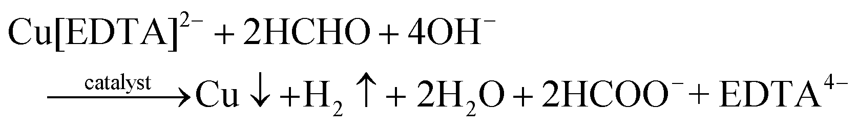 | (1) |
| Cu + 4NaOH + (NH4)2S2O8 → Cu(OH)2 + 2Na2SO4 + 2NH3↑ + 2H2O | (2) |
| Cu(OH)2 + FeCl2 + O2 → FeOOH + [CuClx]1−x + H3O+ | (3) |
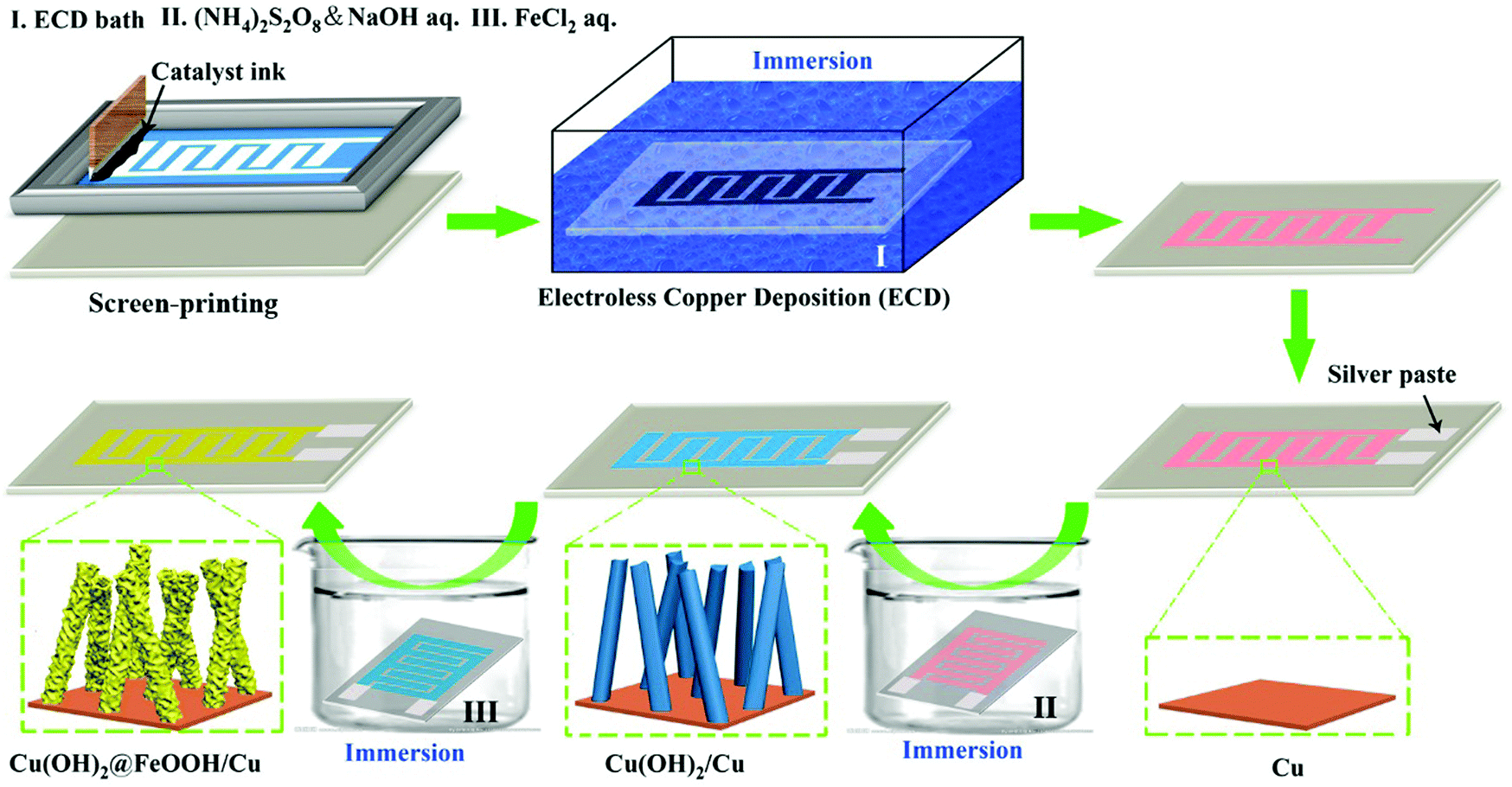 | ||
| Fig. 1 Schematic illustration of the fabrication of interdigitated copper electrodes with an array of Cu(OH)2@FeOOH NTs. | ||
Assembly and electrochemical measurement of MSCs
The patterned copper electrodes with an array of Cu(OH)2@FeOOH NTs were assembled into in-plane MSC energy storage devices by the following steps. Firstly, a gel electrolyte was prepared by a modified method.50 In brief, [EMIM][BF4] ionic liquid and fumed silica (SiO2) nanopowder in a weight ratio of 1:1 were mixed in a motor and milled until a semitransparent paste formed. Subsequently, the as-obtained gel electrolyte was uniformly coated on the electrodes. Finally, the planar MSCs were encapsulated by a mixture of the PDMS prepolymer and curing agent in a weight ratio of 10:1 followed by curing for 2 h at 80 °C.
Characterization
The surface and cross-sectional morphologies of the relevant materials were characterized by field emission scanning electron microscopy (FE-SEM, FEI Nova NanoSEM 450). The structures of the as-synthesized electrochemically active materials were characterized by transmission electron microscopy (TEM, Tecnai G2F30, FEI) and X-ray diffraction (XRD, Rigaku D/max 2500, Japan) with Cu Kα radiation. X-ray photoelectron spectroscopy (XPS, PHI-1800, Japan) was used to determine the surface elemental composition and chemical state of the as-synthesized materials. The electrical resistances of the copper coatings were measured with a Keithley 2000 multimeter with four-point probes. The surface wettability of the PI substrate by water and that of the electrodes by the electrolyte were characterized using a contact angle instrument (Attension Theta optical tensiometer). The Brunauer–Emmett–Teller (BET) specific surface areas of the electrochemically active materials were measured using a Micromeritics ASAP 2020 analyzer at 77 K.A tape test51,52 was used to characterize the adhesion between the as-prepared copper coating and the PI substrate. In detail, five parallel copper lines with lengths of 5 cm and widths and separations of 200 μm were fabricated on the PI substrate and attached firmly with 3M 600 tape, which was subsequently peeled off in a direction vertical to the film.
Electrochemical measurements, including cyclic voltammetry (CV), electrochemical impedance spectroscopy (EIS) tests and galvanostatic charge–discharge (GCD) measurements, were conducted with an electrochemical workstation (Zennium Zahner, Germany) at room temperature. The EIS spectra were recorded in the frequency range from 100 kHz to 0.01 Hz. The calculations of the specific capacitance, energy density and power density of the MSCs are provided in the ESI.†
Results and discussion
Fabrication and properties of copper current collectors
The upper half of Fig. 1 illustrates the process used for patterning the interdigitated copper current collector on a flat substrate. Clearly, this process not only exploits the advantage of the precision of printed electronics (PE) but also produces a highly conductive copper coating, which is difficult to achieve with conductive inks. In particular, by this technique copper can be formed into various patterns, including interdigitated electrodes and common conducting tracks, as shown in Fig. 2a–d and Fig. S1d–f (ESI†). In this way, the fabrication of the current collector for in-plane MSC devices and the preparation of the copper circuit can be closely integrated, which greatly simplifies the integration of in-plane MSC devices into the microelectronic system based on the copper circuit. In addition, the advantages of the copper current collector and copper-patterning process are conspicuous in many other respects. Firstly, in comparison with current collectors fabricated from carbon, gold, nickel and conductive inks, a copper-based metallic current collector combines the advantages of a low material cost and high electrical conductivity. Furthermore, as summarized in Table S1 (ESI†), in comparison with commonly used patterning techniques such as photolithography, wet etching, magnetron sputtering and laser etching, the fabrication of the catalytically deposited copper current collector can be achieved by a more facile process with lower requirements in terms of equipment.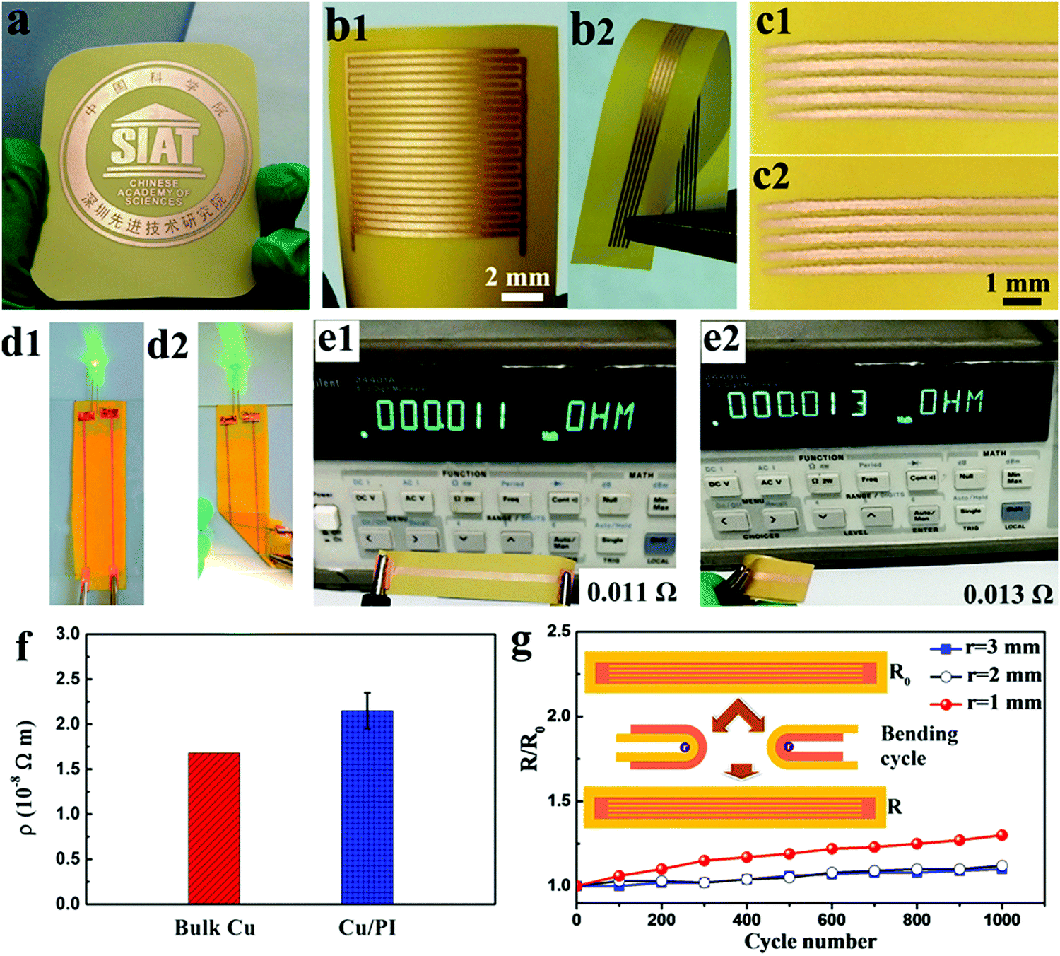 | ||
| Fig. 2 Digital images of electroless copper pattern deposited on (a) EPL and (b) PI. (c) Digital images of copper tracks on PI (c1: before and c2: after the tape test). Cu/PI integrated with (d) an LED and (e) a resistance instrument in the normal and folded states. (f) Bulk electrical resistivity of bulk copper and the as-fabricated copper coatings on PI. (g) Curves of the normalized electrical resistance (R/R0) vs. number of bending cycles for the as-fabricated copper tracks on PI. (Inset in panel g) Schematic of bending test on the as-fabricated copper tracks. | ||
The formation of the electroless copper coating comprises the deposition of metallic copper, in which copper ions are gradually reduced by formaldehyde in the presence of a catalyst, which acts as the medium that transfers electrons from the reducing agent to the copper ions (eqn (1)).23 Firstly, copper is gradually deposited on the area loaded with the catalyst, and the surface resistance sharply decreases as the deposited copper passes from a discrete to a continuous state (Fig. S2 and S3, ESI†). When the catalyst layer is fully coated by the deposited copper, copper continues to be deposited under the effect of autocatalysis by copper, and the surface resistivity gradually decreases with an increase in the thickness of the coating. The bulk electrical resistivity of the copper coating is determined using the following equation:
| ρ = Rsd | (4) |
The digital photos in Fig. 2a and b show as-fabricated copper patterns on a typical rigid epoxy laminate (EPL) and a flexible substrate (PI), respectively. As a substrate for flexible printed circuits (FPCs) commonly used in industry, PI film is used in the further fabrication of flexible in-plane MSCs. As shown in Fig. S5 (ESI†), the PI substrate that is used has a porous surface microstructure that can promote the discharge of H2 produced in the ECD reaction and can thereby effectively prevent corrugation and stripping of the copper coating. Furthermore, as shown in Fig. S6 (ESI†), the contact angle between H2O and the PI substrate decreased greatly from 117.5 ± 0.5° to 7.0 ± 0.3° after surface modification of the substrate, which enabled better bonding between the deposited copper and the PI substrate. As a consequence, the deposited copper coating adhered tightly to the PI film with no signs of stripping after the tape test (Fig. 2c1 and c2). Moreover, the high conductivity of the copper coating, which was comparable to that of the bulk copper, indicated the high compactness of the copper coating. It can be observed from Fig. 3a–c that the copper coating had a compact surface morphology without gaps and voids. In general, high compactness of the copper coating and strong adhesion between the coating and the substrate can contribute to high flexibility of the copper coating. To determine the mechanical stability of the as-deposited copper coating, we fabricated copper tracks on the flexible PI substrate (Cu/PI), which were integrated with an LED (3 V) and a resistance instrument, respectively, to observe the difference in the performance of the copper tracks between the normal and folded states. As shown in Fig. 2d and e, the integrated LED exhibited an inconspicuous change in brightness and the Cu/PI tracks exhibited a slight increase in electrical resistance (from 0.011 Ω to 0.013 Ω) after folding, which indicated that the Cu/PI tracks had high mechanical stability. In order to systematically characterize the flexibility of the as-fabricated copper tracks, a bending test was conducted, as illustrated in the schematic in the inset of Fig. 2g. In detail, five parallel copper lines with lengths of 5 cm and widths of 200 μm were fabricated on the PI substrate and were bent at different radii of curvature for 1000 cycles to record the changes in electrical resistance. As shown in Fig. 2g, the flexibility can be characterized using curves of R/R0vs. the number of bending cycles, where R and R0 are the electrical resistances of the flexible copper circuits after and before the bending tests, respectively. It can be observed from the curves in Fig. 2g that the resistance of Cu/PI increased only slightly after 1000 bending cycles at different radii of curvature, which confirmed that the flexibility of Cu/PI is high. In addition to a PI film, a copper pattern can also be plated on many other flexible substrates by the copper-patterning technique. Digital photographs and SEM images of Cu patterns on polytetrafluoroethylene (PTFE) film, cotton cloth and waste paper are shown in Fig. S1 (ESI†) and demonstrate the generality and versatility of this copper-patterning method.
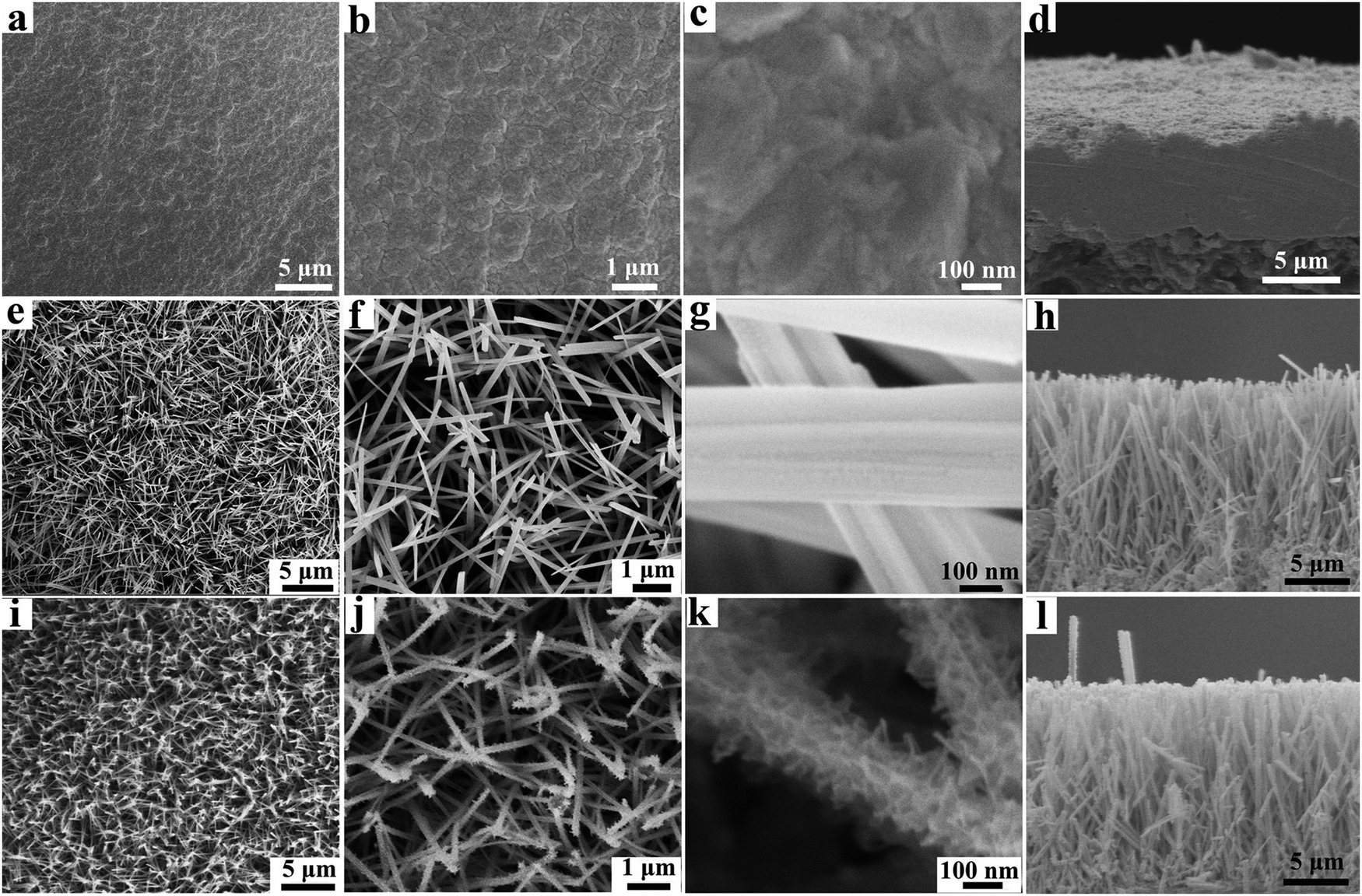 | ||
| Fig. 3 Different large-scale SEM images of the surfaces of (a–c) Cu, (e–g) Cu(OH)2/Cu and (i–k) Cu(OH)2@FeOOH/Cu electrodes. Cross-sectional SEM images of (d) Cu, (h) Cu(OH)2/Cu and (l) Cu(OH)2@FeOOH/Cu electrodes. | ||
The copper pattern is designed in the form of typical interdigitated electrodes for the further fabrication of MSCs. Fig. 2b shows a digital photo of a cellular structure containing 22 interdigitated electrodes with a length (L) of 1 cm. As shown in SEM images (Fig. S7, ESI†) of the as-fabricated interdigitated electrodes on the PI substrate, the widths of the finger electrodes (W) and the distances between adjacent electrodes (d) are 300 μm and 100 μm, respectively. It has been well documented that the capacitance and rate capability of an MSC can be increased by reducing d, because this procedure can not only enlarge the area loaded with the active material but also shorten the ion diffusion pathways between two oppositely charged electrodes.12,20 In our case, by using a screen-printing technique interdigitated electrodes with the lowest d value of 100 μm can be produced without short-circuiting. To investigate the stability of the as-fabricated copper electrodes in the electrolyte ([EMIM][BF4]) that was further used to prepare the gel electrolyte for MSC devices, we conducted stability tests by immersing the as-fabricated copper electrodes into the electrolyte for 48 h, followed by CV scanning from 0 V to 1.5 V for 1000 cycles. As a result, the powder X-ray diffraction (XRD) patterns of the Cu electrodes remained unchanged after the stability tests (Fig. S8, ESI†), which indicates that the as-fabricated copper coating exhibited high stability in the electrolyte.
Fabrication, morphology and structure of array of Cu(OH)2@FeOOH NTs on copper current collector
After the production of the interdigitated copper current collector, a facile in situ conversion method is proposed for loading electrochemically active materials onto the patterned copper current collector. By this method, an array of Cu(OH)2@FeOOH NTs can be grown directly on the interdigitated copper electrodes (Fig. S7c, d and Fig. S9, ESI†). As illustrated in the bottom half of Fig. 1, this synthesis route comprises two in situ conversion steps, both of which are achieved by a simple solution-immersion process at room temperature. Firstly, as evidenced by the SEM images in Fig. 3e–h and the TEM images in Fig. 4a and b, Cu(OH)2 NWs with a diameter of ∼100 nm are formed uniformly on the copper current collector via the reaction described by eqn (2). The as-synthesized Cu(OH)2 NWs are derived from surface copper on the current collector, which contributes to strong binding between the copper current collector and the Cu(OH)2 NWs. Similarly, via another in situ reaction, which is described by eqn (3), the Cu(OH)2 NWs are partially converted into gauze-like FeOOH nanosheets that grow densely throughout the Cu(OH)2 NWs, and the array structure remains complete after the reaction, which can be clearly observed from the SEM images in Fig. 3i–l and the TEM images in Fig. 4e–g and Fig. S10j–l (ESI†). Cross-sectional SEM images of the Cu(OH)2 NWs/Cu and Cu(OH)2@FeOOH NTs/Cu electrodes are shown in Fig. 3h and l, respectively, which indicate that the electrochemically active materials exhibited a one-dimensional array structure with a vertical thickness of up to 14 μm. This structure is beneficial for the in-plane MSC because the increased vertical height of the electrodes can provide a large area of overlap between the two oppositely charged electrodes of the MSC. Furthermore, in comparison with the synthesis of electrochemically active materials by grafting methods, the in situ conversion processes can create highly compact interfaces that lead to reduced interfacial impedance and thereby increase the efficiency of mass and charge transfer during the faradic redox reaction. In addition, the results of cross-sectional energy-dispersive spectroscopy (EDS) mapping of the array of Cu(OH)2@FeOOH NTs in Fig. S11 (ESI†) show that Fe, Cu and O elements were uniformly distributed across the structure, which suggests that the in situ conversion was highly uniform.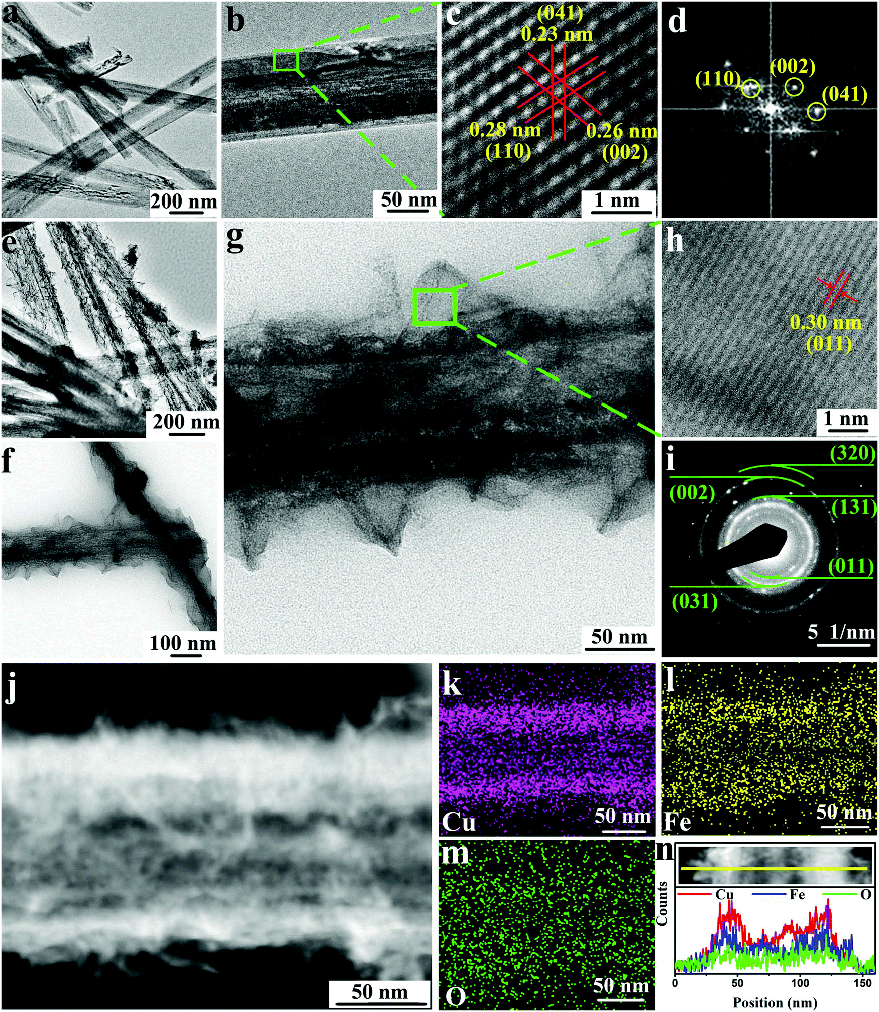 | ||
| Fig. 4 (a and b) TEM images, (c) HRTEM image and (d) FFT-SAED pattern of the Cu(OH)2 NWs. (e–g) TEM images, (h) HRTEM image and (i) SAED pattern of the Cu(OH)2@FeOOH NTs. (j) HAADF-STEM image, (k–m) STEM-EDS maps and (n) STEM-EDS line scan profiles of the Cu(OH)2@FeOOH NTs. | ||
TEM, XRD, X-ray photoelectron spectroscopy (XPS), and BET analysis were employed to characterize the as-synthesized Cu(OH)2@FeOOH structure in more detail. The formation of Cu(OH)2 and FeOOH can be preliminarily evidenced by the occurrence of a surface color change (Fig. S10 and S12, ESI†) and fully confirmed by XRD patterns (Fig. 5a), high-resolution TEM (HRTEM) images (Fig. 4c, h and Fig. S13, ESI†) and selected-area electron diffraction (SAED) analysis (Fig. 4d and i). The HRTEM image in Fig. 4c shows clear lattice fringes with d-spacings of 0.28 nm, 0.26 nm and 0.23 nm, which correspond to the (110), (002) and (041) lattice planes, respectively, of orthorhombic Cu(OH)2 (JCPDS no. 72-0140, space group Cmcm), which is closely consistent with the results obtained from the XRD patterns in Fig. 5a. The ring-like selected-area electron diffraction (SAED) pattern in Fig. 4i reveals the polycrystalline structure of FeOOH, and the diffraction rings from the inside to the outside can be indexed to the (011), (031), (131), (002), and (320) planes, respectively, of orthorhombic FeOOH (JCPDS no. 76-2301, space group Amam). This crystal structure of FeOOH conforms to the results of analysis of the relevant HRTEM image in Fig. 4h and the XRD pattern in Fig. 5a. Furthermore, the hollow structure of the Cu(OH)2@FeOOH NTs can be confirmed by the contrast in mass thickness reflected in the high-magnification TEM image (Fig. 4g) and the high-angle annular dark-field (HAADF)-scanning transmission electron microscopy (STEM) image (Fig. 4j), as well as by the elemental distribution indicated in the STEM-EDS maps (Fig. 4k–m) and the STEM-EDS line scan profiles (Fig. 4n). According to the above analysis, it can be confirmed that the Cu electrode with the array of Cu(OH)2@FeOOH NTs was fabricated successfully, and the structural characteristics of the as-synthesized products are illustrated in Fig. S14 (ESI†).
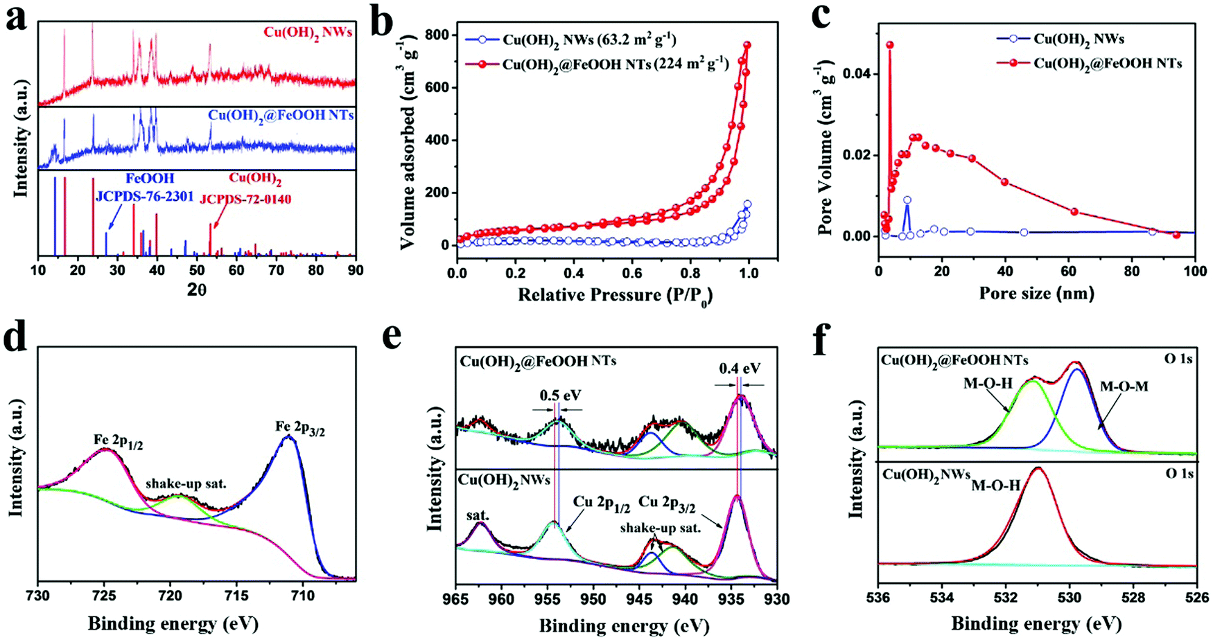 | ||
| Fig. 5 (a) XRD patterns, (b) N2 adsorption–desorption isotherms and (c) Barrett–Joyner–Halenda (BJH) pore size distributions of the Cu(OH)2 NWs and Cu(OH)2@FeOOH NTs. (d) Fe 2p XPS spectrum of the Cu(OH)2@FeOOH NTs. (e) Cu 2p and (f) O 1s spectra of the Cu(OH)2 NWs and Cu(OH)2@FeOOH NTs. | ||
No foreign peaks were present in the XRD patterns (Fig. 5a) and the XPS survey spectra (Fig. S15, ESI†) of the Cu(OH)2 NWs and the Cu(OH)2@FeOOH NTs, which suggests that the products were synthesized in high purity. The corresponding high-resolution XPS spectra shown in Fig. 5d–f provide information about the chemical states of the surface elements in the products. As shown in Fig. 5e, typical shake-up peaks are present in the Cu 2p spectra of the Cu(OH)2 and Cu(OH)2@FeOOH structures, which indicates the presence of Cu(II).53,54 Moreover, the shift between the Cu 2p peaks of the Cu(OH)2 NWs and the Cu(OH)2@FeOOH NTs reveals that the introduction of FeOOH affected the electronic structure of Cu(OH)2, which suggests that strong binding occurred between Cu(OH)2 and FeOOH in the Cu(OH)2@FeOOH structure. This result can be attributed to the in situ conversion approach, which facilitates binding between the product and the precursor. Fig. 5d shows the Fe 2p spectrum of the Cu(OH)2@FeOOH structure, in which there are two dominant peaks at 710.8 eV and 724.5 eV, which can be ascribed to the binding energies of Fe 2p3/2 and Fe 2p1/2, respectively, and the distinct shake-up satellite peak at 719.2 eV is characteristic of Fe(III).55,56 In addition, the presence of FeOOH is also reflected in the O 1s spectra of the Cu(OH)2 NWs and the Cu(OH)2@FeOOH NTs (Fig. 5f). As shown in Fig. 5f, the O 1s spectrum of the Cu(OH)2@FeOOH NTs can be fitted to two main constituent peaks, which correspond to different oxygen-containing species including M–O–H and M–O–M (M: Fe or Cu), whereas the O 1s spectrum of the Cu(OH)2 NWs can only be fitted to a single peak, which corresponds to M–O–H groups. This result closely conforms to the structures of the products, because M–O–M groups are present in FeOOH rather than in Cu(OH)2. As shown in Fig. S10 and S16 (ESI†), the hierarchical structure and composition of Cu(OH)2@FeOOH vary at different stages of the reaction described by eqn (3). With the progress of the reaction, Cu(OH)2 is gradually converted into gauze-like FeOOH nanosheets. This variation greatly influences the performance of the MSC, which will be discussed in detail below. The structure of the Cu(OH)2@FeOOH NTs discussed above is obtained when the reaction has proceeded for 1 h. In general, this structure has a characteristic large specific surface area. N2 adsorption/desorption measurements were carried out to determine the specific surface area and porosity of the Cu(OH)2@FeOOH NTs quantitatively. Fig. 5b shows the N2 adsorption/desorption isotherms of the Cu(OH)2 NWs and the Cu(OH)2@FeOOH NTs, which correspond to the type IV (IUPAC classification) isotherm that is characteristic of mesoporous materials. As evidenced by the Barrett–Joyner–Halenda (BJH) pore size distribution (Fig. 5c) and HRTEM images (Fig. S13, ESI†), both the Cu(OH)2 NWs and the Cu(OH)2@FeOOH NTs were formed with a porous structure. It can be concluded from Fig. 5b and c that, in comparison with the Cu(OH)2 NWs precursor (SBET = 63.2 m2 g−1), the Cu(OH)2@FeOOH NTs exhibited a greater specific surface area (SBET = 224 m2 g−1), a larger pore volume and a wider pore size distribution. The unique morphology and hollow porous structure of the Cu(OH)2@FeOOH NTs could provide abundant reactive sites, increase the efficiency of ion diffusion, and maintain the integrity of the electrodes by releasing the strain produced during the faradic redox reaction.46 Therefore, the as-synthesized Cu(OH)2@FeOOH NTs are suitable in terms of structure to be electrochemically active materials for supercapacitors.
Electrochemical properties of the assembled MSCs
The energy density of the in-plane MSC energy storage devices is largely determined by the amount of electrochemically active material per unit area and the volume of the energy storage devices, which can be controlled by the time for which the copper electrodes are immersed in the aqueous solution of NaOH and (NH4)2SO3 (eqn (2)). Fig. S17 (ESI†) shows GCD curves for MSCs fabricated with copper electrodes with immersion times ranging from 1 to 9 minutes, of which the MSC fabricated with copper electrodes with an immersion time of 5 minutes exhibited the highest capacitance. As the in situ conversion reaction proceeded during the first 5 minutes of immersion (eqn (2)), the Cu(OH)2 NWs that grew on the copper surface underwent a transformation from quite sparse and thin to highly dense and thick (Fig. S18a–e, ESI†), and the specific capacitance of the corresponding MSCs also increased (Fig. S17, ESI†). Upon further immersion, the Cu(OH)2 NWs no longer became thicker, and the one-dimensional array structure was destroyed completely at an immersion time of 9 minutes, which can be evidenced by the surface morphology in the SEM images shown in Fig. S18g and h (ESI†). This transformation not only resulted in a decrease in specific capacitance (Fig. S17, ESI†) but also hindered the further conversion into FeOOH. Therefore, the optimal time for which the copper electrodes are immersed in the aqueous solution of NaOH and (NH4)2SO3 is determined to be 5 minutes. Furthermore, in order to identify the optimal coating of FeOOH on the Cu(OH)2@FeOOH composite used as the electrochemically active material in MSCs, we conducted time-dependent experiments by controlling the time for which the Cu(OH)2/Cu electrodes were immersed in the aqueous solution of FeCl2 (eqn (3)). For illustrative purposes, the copper electrodes with electrochemically active materials obtained at different immersion times are denoted as Cu(OH)2/Cu for 0 h, Cu(OH)2@FeOOH-1/Cu for 0.5 h, Cu(OH)2@FeOOH-2/Cu for 1 h, Cu(OH)2@FeOOH-3/Cu for 1.5 h and Cu(OH)2@FeOOH-4/Cu for 2 h, respectively. These as-fabricated Cu(OH)2@FeOOH/Cu electrodes were further assembled into MSCs by being coated with the gel electrolyte and packaged with PDMS, as shown in the architecture in Fig. 6a, for electrochemical measurements. The specific capacitances of the as-fabricated MSCs were compared by GCD tests. As shown in the GCD curves in Fig. S19 (ESI†), the MSC fabricated with the Cu(OH)2@FeOOH-2/Cu electrode exhibited the highest capacitance among the as-fabricated MSCs. The specific capacitance increased greatly during the first hour of immersion, whereas a steep decline was observed with a further increase in the immersion time. This phenomenon was analyzed from such aspects as morphology, structure (SEM, TEM), specific surface area (BET), wettability of the electrode surface by the electrolyte (contact angle) and electrochemical impedance spectroscopy (EIS). As shown in Fig. S10 (ESI†), during the first 1 h of immersion, the structure of the Cu(OH)2 NWs was transformed gradually into the hierarchical structure of the Cu(OH)2@FeOOH NTs, together with a great increase in the BET specific surface area (Fig. 5b and Fig. S20, ESI†), an increase in pore volumes and a widening of the pore size distribution (Fig. 5c). The increased specific surface area and well-developed porous structure of the electrochemically active material facilitate enhancements in the performance of MSCs. Furthermore, as shown in Fig. S21 (ESI†), the contact angle between the electrode surface and the electrolyte decreased from 18.9 ± 0.7° for Cu(OH)2/Cu to 0° for Cu(OH)2@FeOOH-2/Cu. The enhanced wettability by the electrolyte is conducive to ion diffusion in the faradic redox process, which can be evidenced by EIS curves for the as-fabricated MSCs (Fig. S22, ESI†). As shown in Fig. S22 (ESI†), the slope of the EIS curves in the low-frequency range increased with an increase in the immersion time from 0 to 1 h, which indicates a decrease in the Warburg impedance (ZW) and an increase in the ion diffusion efficiency of the corresponding MSC. Moreover, the hybrid Cu(OH)2@FeOOH structure used as the electrochemically active material contains both positive (Cu(OH)2) and negative (FeOOH) electrode materials, which may result in an MSC that is similar to an asymmetric supercapacitor so as to achieve an enhancement in performance. With the prolongation of the immersion time from 1 h to 2 h, more FeOOH nanosheets were formed, with extensive agglomeration and damage to the array structure (Fig. S10, ESI†). Although the proportion of the gauze-like FeOOH continued to increase (Fig. S16, ESI†), there was no substantive change in the specific surface area of the Cu(OH)2@FeOOH structure, as shown by the BET curves in Fig S18. In addition, the EIS curves in Fig. S22 (ESI†) show that the corresponding equivalent series resistance (Rs), charge transfer resistance (Rct) and ZW increased greatly with an increase in the immersion time from 1 h to 2 h. It can be deduced that the excessive accumulation of FeOOH nanosheets causes an increase in the internal resistance of the MSC device and hinders charge and mass transfer in the faradic redox reaction. From the above results and analysis, the Cu(OH)2@FeOOH-2/Cu electrodes can be confirmed to be the optimal choice for MSCs.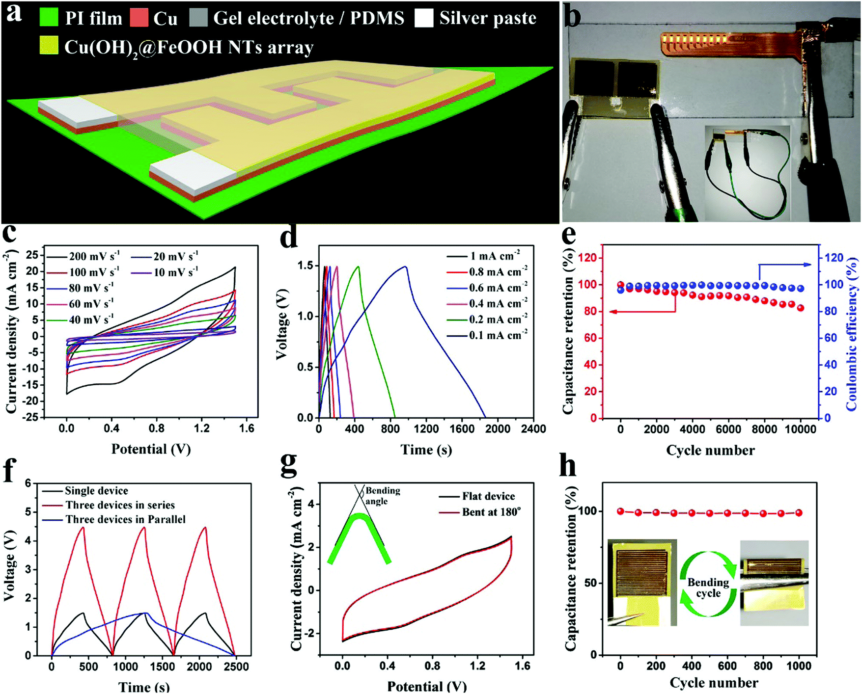 | ||
| Fig. 6 (a) Architecture of an assembled MSC. (b) Digital image of 10 light-emitting diodes (LEDs) powered by two MSCs connected in series. (c) CV curves for MSCs recorded at different scan rates ranging from 10 to 200 mV s−1. (d) Galvanostatic charge–discharge curves for MSCs at different current densities ranging from 0.1 to 1 mA cm−2. (e) Cycling performance of MSCs at a constant charge/discharge current density of 0.2 mA cm−2. (f) Galvanostatic charge–discharge curves (current density = 0.2 mA cm−2) for MSCs connected in series or parallel. (g) Comparative CV curves for MSCs before and after bending at 180°. (h) Capacitance retention as a function of the number of bending cycles at a current density of 0.2 mA cm−2; the inset shows a device in the normal and bent states. | ||
The electrochemical performance of MSCs fabricated with the optimal Cu(OH)2@FeOOH-2/Cu interdigitated electrode was further examined by CV and GCD tests. Fig. 6c shows the CV curves for MSCs recorded at different scanning rates ranging from 10 mV s−1 to 200 mV s−1. These CV curves display obvious redox peaks, which suggest the occurrence of a pseudocapacitive reaction. High areal and volumetric capacitances, as calculated from the GCD curves (Fig. 6d), of up to 58.0 mF cm−2 and 32.2 F cm−3, respectively, were achieved at 1 mA cm−2, with a retention of about 70% (31.4 mF cm−2; 17.4 F cm−3) when the current density was increased to 10 mA cm−2. This high rate capability can be ascribed to the low values of Rct and Zw, as observed from the Nyquist plot in Fig. S22 (ESI†) (Cu(OH)2@FeOOH-2). The as-fabricated MSCs can be easily connected in series or parallel via the design of the patterns in the printing step, and thus the voltage and current of the MSCs can be easily controlled. For instance, the GCD curves for a single MSC and three MSCs in series and in parallel are shown in Fig. 6f, from which the device in which three MSCs were connected exhibited a capacitance that was more than three times that of the single device, and the increment in capacitance was represented by the widening of the voltage window for the device in series and the increase in the GCD time for the device in parallel. Fig. 6b shows that two MSC devices connected in series successfully powered 10 small LEDs. Moreover, as shown in Fig. 6e, the as-fabricated MSCs retained about 82% of their capacitance and a coulombic efficiency of nearly 97% after being charged and discharged at 0.2 mA cm−2 for 10000 cycles, which indicates excellent cycling stability and highly reversible charge storage. As shown in Fig. 6g, CV curves for an as-fabricated MSC in the flat and bent states (180°) were recorded for comparison, from which it can be observed that the profiles of the two CV curves nearly overlap, which suggests that the mechanical stability of the as-fabricated MSC was high. Furthermore, to determine the flexibility of MSCs, we conducted a bending test by bending the devices at 180° for 1000 cycles to record the variation in capacitance. It can be observed from Fig. 6g that the specific capacitance of the MSCs remained at nearly 100% of the initial value after 1000 bending cycles, which suggests that the flexibility of the MSCs was high. The desirable flexibility of the MSCs could be attributed to the high quality of the electroless copper coating that was deposited and the highly compact interfaces, including Cu/PI, Cu(OH)2/Cu and FeOOH/Cu(OH)2.
The areal energy densities of the as-fabricated in-plane MSCs and other very recently reported MSC energy storage devices are summarized in a Ragone plot (Fig. 7) and Table S1 (ESI†) for comparison. The as-fabricated Cu(OH)2@FeOOH/Cu MSCs exhibited a high areal energy density of up to 18.07 μW h cm−2, which exceeds those of most reported MSCs, including both carbon-based electrical double-layer MSCs and pseudo-MSCs, such as 0.38 μW h cm−2 for a 3D graphene MSC produced by CVD,20 3.88 μW h cm−2 for an Ni@MnO2 nanocoral MSC,35 13.1 μW h cm−2 for an rGO-PEDOT/PSS MSC,12 and 8.05 μW h cm−2 for an MnO2//PPy MSC.37 Although the MSCs are inferior to recently reported ultra-thick MSCs fabricated by 3D printing techniques (73.9 μW h cm−2; T = 412 μm; T: thickness of active materials) in terms of areal energy density, their volumetric energy density (10.03 mW h cm−3) is far higher than that of MSCs produced by 3D printing (1.79 mW h cm−3).13 The high performance of the as-fabricated Cu(OH)2@FeOOH/Cu MSCs can be ascribed to the following reasons: the copper current collector is far superior to those based on conductive inks and carbon materials in terms of conductivity; the rationally designed electrochemically active materials (Cu(OH)2@FeOOH NTs) have a hollow porous structure with a large surface area, which could provide abundant reactive sites, increase the efficiency of ion diffusion, and maintain the integrity of the electrodes by releasing the strain produced during the faradic redox reaction; the one-dimensional array structure of the electrochemically active material (array of Cu(OH)2@FeOOH NTs) with a vertical thickness of up to 14 μm provides a large area of overlap between the two oppositely charged electrodes of the MSCs; and the in situ conversion procedure creates highly compact interfaces, including Cu/Cu(OH)2 and Cu(OH)2/FeOOH, which can effectively reduce the interfacial contact resistance.
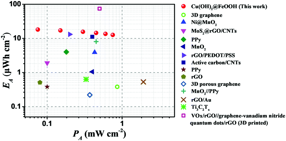 | ||
| Fig. 7 Ragone plot for the as-fabricated Cu(OH)2@FeOOH/Cu MSCs compared with a number of recently reported MSCs, including a 3D graphene MSC,20 an Ni@MnO2 MSC,35 an MoS2@rGO/CNTs MSC,57 a PPy film MSC,2 an MnO2 MSC,36 an rGO/PEDOT/PSS MSC,12 an active carbon MSC,14 a PPy NWs MSC,30 an rGO MSC,58 a 3D porous graphene MSC,9 an MnO2//PPy MSC,37 an rGO/Au MSC,18 a Ti3C2Tx MSC59 and a VOx/rGO//graphene-vanadium nitride quantum dots/rGO MSC.13 | ||
Conclusions
A facile strategy has been demonstrated for producing high-performance in-plane MSC energy storage devices fabricated with interdigitated copper current collectors with a rationally designed array of Cu(OH)2@FeOOH NTs as active materials. The facility of the fabrication process mainly lies in the patterning technique and the fabrication process of the electrodes. A practical copper-patterning technique based on electroless copper deposition with Ag catalysts was proposed for fabricating current collector patterns. By this technique, interdigitated copper electrodes can be patterned together with a widely used copper circuit on a substrate, which is greatly conducive to the integration of MSCs into microelectronic systems. Furthermore, Cu(OH)2@FeOOH/Cu electrodes were fabricated facilely by a three-step solution-immersion process at room temperature, which is highly practical and promising for development into an industrial flow line production process. The as-fabricated MSCs delivered a high energy density of up to 18.07 μW h cm−2, which can be ascribed to the rationally designed Cu(OH)2@FeOOH/Cu electrodes and the synthesis method based on in situ conversion. The high quality of the electroless copper coating that was deposited and the compact interfaces, including Cu/PI, Cu/Cu(OH)2 and Cu(OH)2/FeOOH, make the MSC devices highly flexible.Conflicts of interest
There are no conflicts to declare.Acknowledgements
This work was financially supported by the National Key R&D Project from Minister of Science and Technology of China (2016YFA0202702), the National Natural Science Foundation of China (No.21203236), Guangdong Department of Science and Technology (2017A050501052), and Shenzhen Research Plan (JCYJ20160229195455154). We also thank Dr Ning Wang (Shenzhen Institutes of Advanced Technology, Chinese Academy of Sciences, Shenzhen, China) for TEM measurement help.Notes and references
- S. Zheng, J. Ma, Z.-S. Wu, F. Zhou, Y.-B. He, F. Kang, H.-M. Cheng and X. Bao, Energy Environ. Sci., 2018, 11, 2001–2009 RSC.
- L. Li, C. W. Fu, Z. Lou, S. Chen, W. Han, K. Jiang, D. Chen and G. Z. Shen, Nano Energy, 2017, 41, 261–268 CrossRef CAS.
- M. Beidaghi and Y. Gogotsi, Energy Environ. Sci., 2014, 7, 867–884 RSC.
- Z. S. Wu, Y. Z. Tan, S. H. Zheng, S. Wang, K. Parvez, J. Q. Qin, X. Y. Shi, C. L. Sun, X. H. Bao, X. L. Feng and K. Mullen, J. Am. Chem. Soc., 2017, 139, 4506–4512 CrossRef CAS PubMed.
- Z. Y. Liu, H. I. Wang, A. Narita, Q. Chen, Z. Mics, D. Turchinovich, M. Klaui, M. Bonn and K. Mullen, J. Am. Chem. Soc., 2017, 139, 9443–9446 CrossRef CAS PubMed.
- P. Zhang, J. Wang, W. Sheng, F. Wang, J. Zhang, F. Zhu, X. Zhuang, R. Jordan, O. G. Schmidt and X. Feng, Energy Environ. Sci., 2018, 11, 1717–1722 RSC.
- N. Kurra, B. Ahmed, Y. Gogotsi and H. N. Alshareef, Adv. Energy Mater., 2016, 6, 1601372 CrossRef.
- K. H. Choi, D. B. Ahn and S. Y. Lee, ACS Energy Lett., 2018, 3, 220–236 CrossRef CAS.
- Y. L. Shao, J. M. Li, Y. G. Li, H. Z. Wang, Q. H. Zhang and R. B. Kaner, Mater. Horiz., 2017, 4, 1145–1150 RSC.
- S.-W. Kim, K.-N. Kang, J.-W. Min and J.-H. Jang, Nano Energy, 2018, 50, 410–416 CrossRef CAS.
- C. Chen, J. Cao, X. Y. Wang, Q. Q. Lu, M. M. Han, Q. R. Wang, H. T. Dai, Z. Q. Niu, J. Chen and S. S. Xie, Nano Energy, 2017, 42, 187–194 CrossRef CAS.
- Y. Q. Liu, B. Weng, Q. Xu, Y. Y. Hou, C. Zhao, S. Beirne, K. W. Shu, R. Jalili, G. G. Wallace, J. M. Razal and J. Chen, Adv. Mater. Technol., 2016, 1, 1600166 CrossRef.
- K. Shen, J. Ding and S. Yang, Adv. Energy Mater., 2018, 8, 180048 Search PubMed.
- K. H. Choi, J. Yoo, C. K. Lee and S. Y. Lee, Energy Environ. Sci., 2016, 9, 2812–2821 RSC.
- K. Wang, W. J. Zou, B. G. Quan, A. F. Yu, H. P. Wu, P. Jiang and Z. X. Wei, Adv. Energy Mater., 2011, 1, 1068–1072 CrossRef CAS.
- Y. Q. Li, X. M. Shi, X. Y. Lang, Z. Wen, J. C. Li and Q. Jiang, Adv. Funct. Mater., 2016, 26, 1830–1839 CrossRef CAS.
- A. Ferris, B. Reig, A. Eddarir, J. F. Pierson, S. Garbarino, D. Guay and D. Pech, ACS Energy Lett., 2017, 2, 1734–1739 CrossRef CAS.
- R. Z. Li, R. Peng, K. D. Kihm, S. Bai, D. Bridges, U. Tumuluri, Z. Wu, T. Zhang, G. Compagnini, Z. Feng and A. Hu, Energy Environ. Sci., 2016, 9, 1458–1467 RSC.
- W. J. Hyun, E. B. Secor, C. H. Kim, M. C. Hersam, L. F. Francis and C. D. Frisbie, Adv. Energy Mater., 2017, 7, 1700285 CrossRef.
- L. Zhang, D. DeArmond, N. T. Alvarez, R. Malik, N. Oslin, C. McConnell, P. K. Adusei, Y. Y. Hsieh and V. Shanov, Small, 2017, 13, 1603114 CrossRef PubMed.
- M. Heon, S. Lofland, J. Applegate, R. Nolte, E. Cortes, J. D. Hettinger, P. L. Taberna, P. Simon, P. H. Huang, M. Brunet and Y. Gogotsi, Energy Environ. Sci., 2011, 4, 135–138 RSC.
- G. Lee, D. Kim, D. Kim, S. Oh, J. Yun, J. Kim, S.-S. Lee and J. S. Ha, Energy Environ. Sci., 2015, 8, 1764–1774 RSC.
- J. Q. Xie, Y. Q. Ji, D. S. Mao, F. T. Zhang, X. Z. Fu, R. Sun and C. P. Wong, ACS Appl. Nano Mater., 2018, 1, 1531–1540 CrossRef CAS.
- S. Wang, Z. S. Wu, S. H. Zheng, F. Zhou, C. L. Sun, H. M. Cheng and X. H. Bao, ACS Nano, 2017, 11, 4283–4291 CrossRef CAS PubMed.
- H. Tan, X. N. Wang, D. D. Jia, P. Hao, Y. H. Sang and H. Liu, J. Mater. Chem. A, 2017, 5, 2580–2591 RSC.
- P. Hao, Z. H. Zhao, Y. H. Leng, J. Tian, Y. H. Sang, R. I. Boughton, C. P. Wong, H. Liu and B. Yang, Nano Energy, 2015, 15, 9–23 CrossRef CAS.
- J. Wang, J. Tang, Y. L. Xu, B. Ding, Z. Chang, Y. Wang, X. D. Hao, H. Dou, J. H. Kim, X. G. Zhang and Y. Yamauchi, Nano Energy, 2016, 28, 232–240 CrossRef CAS.
- D. Sheberla, J. C. Bachman, J. S. Elias, C. J. Sun, Y. Shao-Horn and M. Dinca, Nat. Mater., 2017, 16, 220–224 CrossRef CAS PubMed.
- Y. Huang, H. Hu, Y. Huang, M. S. Zhu, W. J. Meng, C. Liu, Z. X. Pei, C. L. Hao, Z. K. Wang and C. Y. Zhi, ACS Nano, 2015, 9, 4766–4775 CrossRef CAS PubMed.
- M. S. Zhu, Y. Huang, Y. Huang, H. F. Li, Z. F. Wang, Z. X. Pei, Q. Xue, H. Y. Geng and C. Y. Zhi, Adv. Mater., 2017, 29, 1605137 CrossRef PubMed.
- X. L. Li, X. D. Li, J. L. Cheng, D. M. Yuan, W. Ni, Q. Guan, L. Z. Gao and B. Wang, Nano Energy, 2016, 21, 228–237 CrossRef CAS.
- H. Tong, S. H. Yue, L. Lu, F. Q. Jin, Q. W. Han, X. G. Zhang and J. Liu, Nanoscale, 2017, 9, 16826–16835 RSC.
- J. Zhi, H. Cui, Z. Wang and F. Huang, Mater. Horiz., 2018, 5, 691–698 RSC.
- M. R. Lukatskaya, S. Kota, Z. F. Lin, M. Q. Zhao, N. Shpigel, M. D. Levi, J. Halim, P. L. Taberna, M. Barsoum, P. Simon and Y. Gogotsi, Nat. Energy, 2017, 2, 17105 CrossRef CAS.
- Y. J. Lin, Y. Gao and Z. Y. Fan, Adv. Mater., 2017, 29, 1701736 CrossRef PubMed.
- H. B. Hu, Z. B. Pei, H. J. Fan and C. H. Ye, Small, 2016, 12, 3059–3069 CrossRef CAS PubMed.
- R. S. Guo, J. T. Chen, B. J. Yang, L. Y. Liu, L. J. Su, B. S. Shen and X. B. Yan, Adv. Funct. Mater., 2017, 27, 1702394 CrossRef.
- X. H. Xia, Y. Q. Zhang, D. L. Chao, Q. Q. Xiong, Z. X. Fan, X. L. Tong, J. P. Tu, H. Zhang and H. J. Fan, Energy Environ. Sci., 2015, 8, 1559–1568 RSC.
- P. Hao, J. Tian, Y. H. Sang, C. C. Tuan, G. W. Cui, X. F. Shi, C. P. Wong, B. Tang and H. Liu, Nanoscale, 2016, 8, 16292–16301 RSC.
- P. P. Shi, L. Li, L. Hua, Q. Q. Qian, P. F. Wang, J. Y. Zhou, G. Z. Sun and W. Huang, ACS Nano, 2017, 11, 444–452 CrossRef CAS PubMed.
- P. P. Shi, R. Chen, L. Li, J. N. An, L. Hua, J. Y. Zhou, B. Liu, P. Chen, W. Huang and G. Z. Sun, Nanoscale, 2018, 10, 5442–5448 RSC.
- H. H. Xu, X. L. Hu, H. L. Yang, Y. M. Sun, C. C. Hu and Y. H. Huang, Adv. Energy Mater., 2015, 5, 1401882 CrossRef.
- C. Zhang, Y. Huang, S. L. Tang, M. S. Deng and Y. W. Du, ACS Energy Lett., 2017, 2, 759–768 CrossRef CAS.
- Y. Song, T. Y. Liu, B. Yao, M. Y. Li, T. Y. Kou, Z. H. Huang, D. Y. Feng, F. X. Wang, Y. X. Tong, X. X. Liu and Y. Li, ACS Energy Lett., 2017, 2, 1752–1759 CrossRef CAS.
- C. R. Zhu, L. Yang, J. K. Seo, X. Zhang, S. Wang, J. Shin, D. L. Chao, H. Zhang, Y. S. Meng and H. J. Fan, Mater. Horiz., 2017, 4, 415–422 RSC.
- C. Guan, X. M. Liu, W. N. Ren, X. Li, C. W. Cheng and J. Wang, Adv. Energy Mater., 2017, 7, 1602391 CrossRef.
- Y. Rangom, X. Tang and L. F. Nazar, ACS Nano, 2015, 9, 7248–7255 CrossRef CAS PubMed.
- J. H. Kang, J. L. Sheng, J. Q. Xie, H. Q. Ye, J. H. Chen, X. Z. Fu, G. P. Du, R. Sun and C. P. Wong, J. Mater. Chem. A, 2018, 6, 10064–10073 RSC.
- J. Liu, X. J. Xu, R. Z. Hu, L. C. Yang and M. Zhu, Adv. Energy Mater., 2016, 6, 1600256 CrossRef.
- B. S. Shen, R. S. Guo, J. W. Lang, L. Liu, L. Y. Liu and X. B. Yan, J. Mater. Chem. A, 2016, 4, 8316–8327 RSC.
- J. P. Liu, C. Yang, P. C. Zou, R. Yang, C. Xu, B. H. Xie, Z. Y. Lin, F. Y. Kang and C. P. Wong, J. Mater. Chem. C, 2015, 3, 8329–8335 RSC.
- Y. C. Liao and Z. K. Kao, ACS Appl. Mater. Interfaces, 2012, 4, 5109–5113 CrossRef CAS PubMed.
- S. Velu, K. Suzuki, M. Vijayaraj, S. Barman and C. S. Gopinath, Appl. Catal., B, 2005, 55, 287–299 CrossRef CAS.
- C. C. Chusuei, M. A. Brookshier and D. W. Goodman, Langmuir, 1999, 15, 2806–2808 CrossRef CAS.
- T. Yamashita and P. Hayes, Appl. Surf. Sci., 2009, 255, 8194 CrossRef CAS.
- Y. C. Chen, Y. G. Lin, Y. K. Hsu, S. C. Yen, K. H. Chen and L. C. Chen, Small, 2014, 10, 3803–3810 CrossRef CAS PubMed.
- W. Yang, L. He, X. C. Tian, M. Y. Yan, H. Yuan, X. B. Liao, J. S. Meng, Z. M. Hao and L. Q. Mai, Small, 2017, 13, 1700639 CrossRef PubMed.
- X. Pu, M. M. Liu, L. X. Li, S. C. Han, X. L. Li, C. Y. Jiang, C. H. Du, J. J. Luo, W. G. Hu and Z. L. Wang, Adv. Energy Mater., 2016, 6, 1601254 CrossRef.
- C. F. Zhang, M. P. Kremer, A. Seral-Ascaso, S. H. Park, N. McEvoy, B. Anasori, Y. Gogotsi and V. Nicolosi, Adv. Funct. Mater., 2018, 28, 1705506 CrossRef.
Footnote |
| † Electronic supplementary information (ESI) available. See DOI: 10.1039/c8ee01979g |
| This journal is © The Royal Society of Chemistry 2019 |