
 Open Access Article
 This Open Access Article is licensed under a
 Creative Commons Attribution 3.0 Unported Licence
[Ge(TenBu)4] – a single source precursor for the chemical vapour deposition of germanium telluride thin films†
Samantha L.
Hawken
a,
Ruomeng
Huang
 b,
C. H. (Kees)
de Groot
b,
Andrew L.
Hector
a,
Marek
Jura
c,
William
Levason
a,
Gillian
Reid
*a and
Gavin B. G.
Stenning
c
b,
C. H. (Kees)
de Groot
b,
Andrew L.
Hector
a,
Marek
Jura
c,
William
Levason
a,
Gillian
Reid
*a and
Gavin B. G.
Stenning
c
aSchool of Chemistry, University of Southampton, Southampton SO17 1BJ, UK. E-mail: G.Reid@soton.ac.uk
bSchool of Electronics and Computer Science, University of Southampton, Southampton SO17 1BJ, UK
cISIS Neutron and Muon Source, Rutherford Appleton Laboratory, Harwell Science and Innovation Campus, Didcot, OX11 0QX, UK
First published on 23rd November 2018
Abstract
Reaction of activated germanium with nBu2Te2 in THF solution was shown to be more effective for the preparation of the germanium(IV) tellurolate compound, [Ge(TenBu)4], than reaction of GeCl4 with LiTenBu in a 1![[thin space (1/6-em)]](https://www.rsc.org/images/entities/char_2009.gif) :4 molar ratio in THF. The product was characterised by 1H, 13C{1H} NMR spectroscopy and microanalysis and evaluated as a single source precursor for the low pressure chemical vapour deposition of GeTe thin films. Depending upon deposition conditions, either dull grey films (predominantly elemental Te) or highly reflective (GeTe) films were obtained from the pure precursor. Grazing incidence X-ray diffraction shows that the highly reflective films are comprised of the rhombohedral α-GeTe phase, while scanning electron microscopy and energy dispersive X-ray analysis reveal rhomb-shaped crystallites with a 49(1):51(1)% Ge:Te ratio. This structure is also confirmed from Raman spectra. Van der Pauw measurements show ρ = 3.2(1) × 10−4 Ω cm and Hall electrical measurements indicate that the GeTe thin films are p-type, with a mobility of 8.4(7) cm2 V−1 s−1 and carrier concentration of 2.5(2) × 1021 cm−3. The high p-type concentration is most likely a result of the substantial Ge vacancies in its sub-lattice, in line with the EDX elemental ratios.
:4 molar ratio in THF. The product was characterised by 1H, 13C{1H} NMR spectroscopy and microanalysis and evaluated as a single source precursor for the low pressure chemical vapour deposition of GeTe thin films. Depending upon deposition conditions, either dull grey films (predominantly elemental Te) or highly reflective (GeTe) films were obtained from the pure precursor. Grazing incidence X-ray diffraction shows that the highly reflective films are comprised of the rhombohedral α-GeTe phase, while scanning electron microscopy and energy dispersive X-ray analysis reveal rhomb-shaped crystallites with a 49(1):51(1)% Ge:Te ratio. This structure is also confirmed from Raman spectra. Van der Pauw measurements show ρ = 3.2(1) × 10−4 Ω cm and Hall electrical measurements indicate that the GeTe thin films are p-type, with a mobility of 8.4(7) cm2 V−1 s−1 and carrier concentration of 2.5(2) × 1021 cm−3. The high p-type concentration is most likely a result of the substantial Ge vacancies in its sub-lattice, in line with the EDX elemental ratios.
Introduction
The binary IV–VI semiconductor, GeTe, is a promising candidate for a number of technologically important applications,1 including for incorporation into thermoelectric,2,3 ferroelectric4 and spintronic materials,5–7 as well as in solid state memory,8,9 where GeTe is layered alternately with Sb2Te310 in interfacial memory or combined with Sb2Te3 in the ternary Ge2Sb2Te5 (GST-225) alloy.8,9 Its phase change memory applications arise since GeTe has a highly conductive crystalline state, whilst in the amorphous phase it is highly resistive.11 It also exhibits extremely fast switching speeds, as low as 1 ns.12
GeTe is one of the best known p-type thermoelectric materials. However, its relatively low Seebeck coefficient (∼30 μV K−1) due to large p-type carrier concentrations (∼1021 cm−3) has largely affected its thermoelectric properties, leading to a maximum ZT value of 0.7 at 720 K.13 Recently, GeTe-rich alloys such as Ge–Pb–Te, Ge–Sb–Te and GeTe-AgSbTe2 have demonstrated enhanced thermoelectric performance and have generated great interest in further investigating GeTe-based alloys for intermediate temperature thermoelectric applications.14
Crystalline germanium telluride can adopt three distinct phases, α-GeTe, β-GeTe and γ-GeTe.1,15 β-GeTe has a rocksalt structure (Fm![[3 with combining macron]](https://www.rsc.org/images/entities/char_0033_0304.gif) m), and is found only above 630 K.15,16 At lower temperature GeTe exists either in the rhombohedral, distorted rocksalt structure (α-GeTe, Rm) or the orthorhombic structure (γ-GeTe), with the orthorhombic structure prevalent at Te > 51.2%.15 It is the Peierls effect that causes the distortion in the rocksalt structure to form α-GeTe and has important implications in GeTe based phase change memory.17 The outcome is alternating short strong and long weak GeTe bonds aligned in the (111) plane, causing the unit cell to become elongated in this direction.18,19
m), and is found only above 630 K.15,16 At lower temperature GeTe exists either in the rhombohedral, distorted rocksalt structure (α-GeTe, Rm) or the orthorhombic structure (γ-GeTe), with the orthorhombic structure prevalent at Te > 51.2%.15 It is the Peierls effect that causes the distortion in the rocksalt structure to form α-GeTe and has important implications in GeTe based phase change memory.17 The outcome is alternating short strong and long weak GeTe bonds aligned in the (111) plane, causing the unit cell to become elongated in this direction.18,19
Various forms and morphologies of GeTe have been deposited using a range of techniques. GeTe nanowires and single crystals have been grown by vapour liquid solid growth,20,21 while thin films have mostly been produced by sputtering22,23 and molecular beam epitaxy.24,25 Other techniques, including thermal co-evaporation26 and atomic layer deposition (using {(CH3)3Si}2Te and either HGeCl3 or Ge{N[Si(CH3)3]2}2) have also been employed.27 GeTe nanocrystals have also been synthesised from GeCl2·dioxane or Ge{N[Si(CH3)3]2}2 with trioctyl phosphine telluride.28
Chemical vapour deposition (CVD) is a widely used deposition technique for thin films and coatings, with its relatively low cost and scalability being particular attractions, while, unlike PVD, it is not a line-of-sight technique.29 Dual source CVD has been used for the growth of GeTe thin films.30,31 For example, Salicio et al. used Ge(NMe2)4 and TeiPr2 in toluene in a pulsed liquid injection CVD method to produce Te-rich GeTe films (Ge0.79Te1.00).30 For the heavier group 14 metal chalcogenides, SnE2 and SnE (E = S, Se, Te), a range of single source precursors have been developed to deposit either the tin mono- or di-chalcogenide thin film through judicious choice of precursor and/or deposition conditions, e.g. [Sn(SCH2CH2S)2],32 various alkyl tin dithiocarbamates,33 thio/selenoether complexes of SnCl434,35 and tin chalcogenide guanadinato complexes.36 As well as offering increased control of stoichiometry, using single source precursors can offer the added advantage of selective deposition of the binary material onto specific regions of a (lithographically) patterned substrate, as demonstrated for example with Sn(IV) chloride complexes bearing neutral chalcogenoether ligands, such as [SnCl4{nBuE(CH2)nEnBu}] (n = 2, 3).35 This selectivity can be beneficial for particular applications.
However, the lighter GeCl4 is an extremely weak Lewis acid and consequently, complexes of Ge(IV) chloride with neutral chalcogenoether ligands do not exist. Using the more Lewis acidic GeF4, a small number of coordination complexes with neutral dithioethers has been reported, [GeF4{MeS(CH2)2SMe}] and [GeF4{EtS(CH2)2SEt}]. Whilst crystallographic data confirm their distorted octahedral structures, these complexes are very labile, with weak (long) Ge–S bonds,37 and analogues containing the less basic selenoether/telluroether ligands do not seem to be accessible.
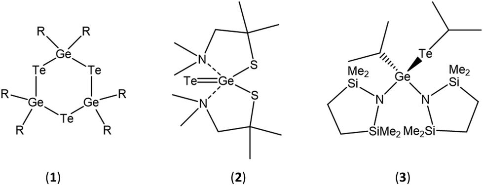
A small number of single source precursors for the deposition of GeTe crystals are reported in the literature, although, with one exception (below), these have not been used for the CVD of GeTe thin films. Gupta et al. synthesised (R2GeTe)3 (R = Et, Bu) (1) from the reaction of Li2Te and R2GeCl2, and thermal decomposition of the precursor in trioctylphosphine at 300 °C resulted in rhombohedral GeTe,38 while Kim et al. showed that thermal decomposition of [Te = Ge(dmampS)2] (2) in hexadecane at 270 °C produced Te-rich rhombohedral Ge40Te57.39
In view of the technologically important applications of GeTe thin films and the paucity of single source precursors for CVD of high quality GeTe films, we report here the development and characterisation of [Ge(TenBu)4] and application of this compound as a single source precursor for the low pressure CVD of highly reflective, crystalline GeTe thin films. Grazing incidence X-ray diffraction (GIXRD), scanning electron microscopy (SEM), energy dispersive X-ray (EDX) and Raman analyses to establish the structural and compositional characteristics of the films, as well as electrical characterisation via van der Pauw and Hall measurements, are discussed.
Results and discussion
Precursor synthesis
Due to the extremely weak Lewis acidity of GeCl4 and the complete absence of any telluroether complexes of germanium in the literature, coordination complexes suitable for use as single source precursors for germanium telluride thin films are not accessible. However, compounds such as the antimony chalcogenolates [MexSb(EnBu)3−x] (E = Se, Te), have previously been synthesised by the direct reaction of LiEnBu with 1/(3 − x) MexSbCl3−x. For x = 0 or 1, these were shown to function as efficient single source precursors for the deposition of Sb2E3 thin films.41 Consequently, the compound, [Ge(TenBu)4] was identified as a possible precursor for GeTe thin film deposition. Two methods were explored for the synthesis of this compound, as illustrated in Scheme 1.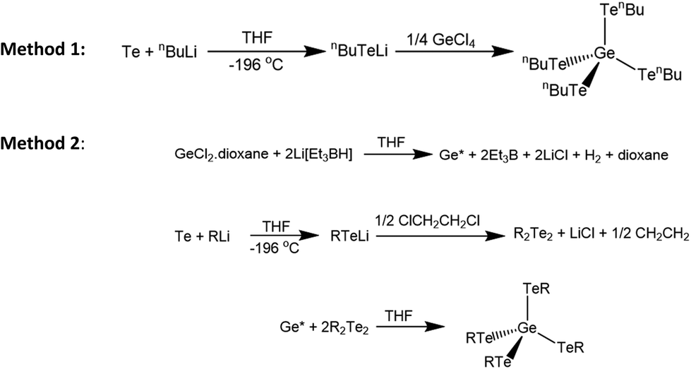 | ||
| Scheme 1 Methods employed for the synthesis of [Ge(TenBu)4]. | ||
Method 1 afforded the product as a viscous dark red oil. Characterisation by 1H and 13C{1H} NMR spectroscopy were consistent with formation of the desired [Ge(TenBu)4] product, together with variable amounts of nBu2Te and nBu2Te2 (13C{1H} and 125Te{1H} NMR evidence). Attempts to separate this mixture by placing it under vacuum, or by distillation, were unsuccessful. Attempts to optimise the synthesis of [Ge(TenBu)4] using Method 1 by adjusting the reaction temperature, reaction times and nBuLi:Te ratio, met with some success, although small amounts of the same Te by-products were always evident, hence an alternative synthesis for this precursor was sought.
Schlecht et al. reported the synthesis of [Ge(EPh)4] (E = Se, Te) by the reaction of activated germanium with Ph2E2 (E = Se, Te).42 Whilst the selenolate derivative was produced in good yield, the germanium tellurolate compound was afforded in only 26% yield. We replicated this synthesis, resulting in a mixture of Ph2Te2 and [Ge(TePh)4] in a ∼40:60 ratio. Separation of the products was achieved by washing the product with ice cold diethyl ether, although this reduced the isolated yield significantly.
In order to obtain a pure sample of the target CVD precursor, [Ge(TenBu)4], the method was adapted (Method 2), using nBu2Te2 in place of Ph2Te2. The nBu2Te2 was first synthesised via the reaction of nBuTeLi with 1,2-dichloroethane. 1,2-Bis(butyltelluro)ethane is unstable and decomposes spontaneously to form nBu2Te2 with elimination of ethene. The resulting nBu2Te2 is a dark red oil and was stored under nitrogen in the freezer. The isolated material was spectroscopically pure by 1H, 13C{1H} and 125Te{1H} NMR analysis.
As the target [Ge(TenBu)4] is an oil, it was expected that separation of this from nBu2Te2 would be more difficult than for the solid [Ge(TePh)4]. It is not possible to know the actual yield of Ge*, however, it can be assumed that the yield of Ge* is not 100%, and therefore a deficit of nBu2Te2 is required for the synthesis to minimise the amount of unreacted nBu2Te2 present in the final product. We found that using only half of the stoichiometric amount of nBu2Te2 in Method 2 resulted, after work-up, in the formation of a dark red oil whose microanalysis was consistent with the proposed [Ge(TenBu)4] formulation. Characterisation by 1H and 13C{1H} NMR spectroscopy also showed that the desired product had been obtained without any nBu2Te2 or nBu2Te by-products, (Table 1, Fig. S1 and S2†). IR spectroscopy showed bands at 238 and 251 cm−1. The former is tentatively assigned to the Ge–Te stretching vibration. Thus, Method 2 appears to provide a more effective for the preparation of pure [Ge(TenBu)4].
| Compound | δ(13C)/ppm | |||
|---|---|---|---|---|
| [Ge(TenBu)4] | 12.90 | 13.53 | 25.29 | 34.53 |
| n Bu2Te | 2.24 | 13.33 | 25.03 | 34.32 |
| n Bu2Te2 | 4.22 | 13.32 | 24.56 | 35.72 |
Monitoring a CDCl3 solution of the [Ge(TenBu)4] by 1H NMR spectroscopy showed that it decomposes slowly over time, producing nBu2Te2. This decomposition was much slower when the [Ge(TenBu)4] was stored under a dry N2 atmosphere in the freezer.
Low pressure CVD of GeTe thin films
Low pressure CVD experiments were undertaken using the precursor produced from both Methods 1 and 2. A typical experiment used ∼50 mg of precursor and PVD SiO2 on Si substrates. Low pressure CVD using the precursor obtained via Method 1 resulted in partial evaporation of the precursor, with some black residue remaining. Deposition occurred onto the substrate closest to the precursor, producing a silvery, very reflective film, while at the edge of the film closest to the precursor, the deposit was a dull grey.Grazing incidence X-ray diffraction (XRD) analysis, as shown in Fig. 1, revealed that the reflective film was phase pure rhombohedral (α-GeTe), with space group R3mH. Refined lattice parameters (a = 4.145(2), c = 10.620(8) Å) are consistent with those reported in the literature (a = 4.156(3), c = 10.663(5);43a = 4.164(2), c = 10.69(4)).44 Crystallite sizes were estimated from the diffraction data peak widths at ∼200 nm. An enhancement to the intensity of the 003 reflection (0.3× the intensity of the 02−2 compared with 0.06× in the standard pattern) suggests some preferred orientation of this axis of the crystallites to the substrate surface normal. This is not seen in the higher angle 006 peak, as expected, since in grazing incidence geometry the diffraction vector of this peak is inclined further from the surface normal and would be less affected by this crystallite preferred orientation. Further, the dull grey region was shown by XRD to be formed of a mixture of GeTe and crystalline tellurium (Fig. S3†).
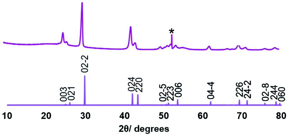 | ||
| Fig. 1 XRD pattern obtained for the GeTe film deposited on PVD SiO2 from [Ge(TenBu)4] synthesised via Method 1 (top) and an indexed literature XRD pattern for bulk GeTe (bottom).45 The peak due to the Si underlying the SiO2 in the substrate is marked *. | ||
Scanning electron microscopy (SEM) analysis of the GeTe film revealed a uniform array of crystallites. The film also appears to be very smooth, and therefore reflective. A cross sectional SEM image shows that the film has a thickness of ∼100 nm (Fig. 2). This is smaller than the crystallite size indicated from the diffraction data and, combined with the observed preferred orientation, it is likely that the crystallites have a tendency to grow as platelets in the a/b plane as observed in the thicker films (Fig. 5).
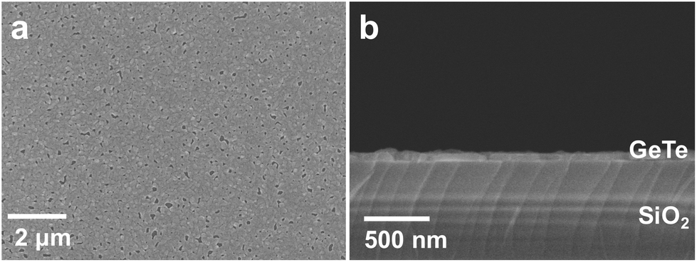 | ||
| Fig. 2 Top view (a) and cross section (b) SEM images of a GeTe film deposited onto PVD SiO2 from [Ge(TenBu)4] synthesised by Method 1. | ||
Energy dispersive X-ray (EDX) analysis showed the Ge:Te ratio was 49(1):51(1), with no impurities detected (Fig. 3a). GeTe is often found in an imperfect stoichiometry due to intrinsic point defects (dominated by Ge vacancies).46,47 The Raman spectrum from the film (Fig. 3b) shows three peaks at ∼122 cm−1, ∼140 cm−1 and ∼155 cm−1, which is consistent with those reported in the literature.25,48–50 Peak A at ∼122 cm−1 can be assigned to the symmetric stretching vibrations of GeTe4 tetrahedra (A1g) and peak C, at ∼155 cm−1, corresponds to the vibrations of Ge atoms distinct from their distorted octahedral sites. The additional peak at ∼140 cm−1 (B) potentially originates from the aging effect.50,51
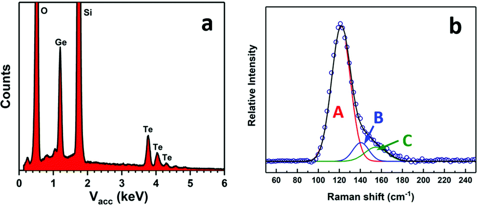 | ||
| Fig. 3 EDX spectrum (a) and Raman spectrum (b) from a GeTe film deposited onto PVD SiO2 using [Ge(TenBu)4] prepared via Method 1. | ||
The resistivity of the GeTe film was determined by van der Pauw measurements, giving ρ = 3.2(1) × 10−4 Ω cm, which compares well with other reported values (ρ = 1.4 × 10⁻⁴ Ω cm).13 Hall measurements revealed that the GeTe film is a p-type semiconductor with a mobility of 8.4(7) cm2 V−1 s−1 and carrier concentration of 2.5(2) × 1021 cm−3. This high p-type concentration is a result of the substantial Ge vacancies in its sub-lattice, as also suggested by the EDX results.52
Since it proved difficult to obtain GeTe films using the precursor from Method 1 without co-deposition of elemental Te, CVD experiments were performed under similar conditions using the pure [Ge(TenBu)4] compound obtained via Method 2. These also led to partial evaporation of the precursor with some black residue remaining. Good coverage of the substrates was observed, with dull grey films on the two substrates nearest the precursor (cooler region, substrate T ∼300–330 °C), shown to be dominated by elemental Te, while films that were deposited further into the hot zone were highly reflective and silver in colour. Characterisation of the latter (substrate T ∼360–400 °C) by grazing incidence XRD showed that only rhombohedral GeTe was present (space group R3mH), with no trace of crystalline tellurium (Fig. 4). Lattice parameters (a = 4.1565(10), c = 10.646(3) Å) also match well with the literature data.41,42 We note that low pressure CVD experiments using [Ge(TePh)4] did not result in any significant film deposition, likely due to a combination of the stronger Te–C(aryl) bonds, the lower volatility of this compound, coupled with the its inability to undergo a low energy decomposition pathway, such as β-hydride elimination.
 | ||
| Fig. 4 XRD pattern obtained for the GeTe film deposited on PVD SiO2 from [Ge(TenBu)4] synthesised via Method 2 (top) and an indexed literature XRD pattern for bulk GeTe (bottom).53 The peak due to the Si underlying the SiO2 in the substrate is marked *. | ||
SEM analysis (Fig. 5) shows much larger crystallites (∼1–2 microns in diameter) than those in the film deposited from the precursor from Method 1. The film is around 1.5–2 μm thick, in line with the typical crystallite dimensions.
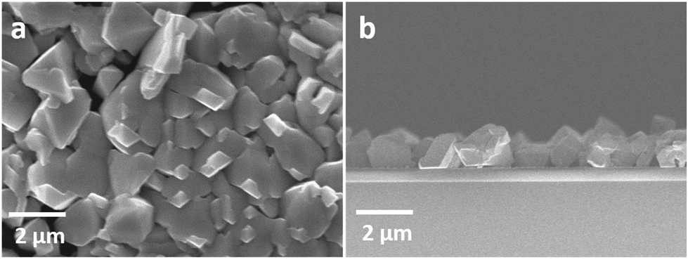 | ||
| Fig. 5 Top view (a) and cross section (b) SEM images of a GeTe film deposited onto PVD SiO2 from [Ge(TenBu)4] synthesised via Method 2. | ||
EDX analysis revealed both germanium and tellurium to be present, with no indication of any residual carbon (Kα = 0.277 keV), as shown in Fig. 6a. Quantification of the germanium and tellurium peaks gave a ratio of 49(1):51(1) Ge:Te. Raman spectra from the films (Fig. 6b) also show three peaks positioned at ∼124 cm−1, ∼141 cm−1 and ∼156 cm−1. The slight upshift of the phonon modes compared with that in Fig. 3 can be ascribed to the increase of the crystal size which also leads to peak narrowing of the Raman spectra.48 The discontinuity of the films obtained using the precursor from Method 2 precluded electrical measurements.
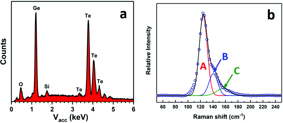 | ||
| Fig. 6 EDX analysis (a) and Raman spectrum (b) from a GeTe film deposited onto PVD SiO2 from [Ge(TenBu)4] prepared via Method 2. | ||
Experimental
IR spectra were recorded as Nujol mulls or neat thin films between CsI plates using a PerkinElmer Spectrum 100 instrument over the range 4000–200 cm−1. 1H and 13C{1H} NMR spectra were recorded from solutions in CDCl3 or CD2Cl2 on a Bruker AV400 spectrometer and referenced to TMS via the residual protio-solvent resonance. 125Te{1H} NMR spectra were recorded from solutions in CD2Cl2 on a Bruker AV400 spectrometer and referenced to external neat TeMe2. Microanalytical results were obtained from Medac Ltd.Substrate preparation
PVD SiO2 films with a thickness of either 500 nm or 1 μm were deposited on silicon wafers by the medium frequency magnetron sputtering method using a pure Si (99.99% purity) target with a DC power of 2000 W in an O2/Ar atmosphere. The O2 and Ar flow rates were maintained at 20 and 40 SCCM respectively. With a drive speed of 180 rpm, the deposition rate was 0.3 nm s−1.Thin film characterisation
Grazing incidence X-ray diffraction patterns were collected using a Rigaku SmartLab system, with CuKα X-rays, a 2θ scan range of 10–80° and an incident angle of 1°. The XRD patterns were matched to literature patterns to determine the crystalline phase.54 Lattice parameters were calculated by optimisation of the fit of grazing incidence or in plane XRD patterns in PDXL2.55 Scanning electron microscopy (SEM) images and energy dispersive X-ray (EDX) measurements were obtained using a JEOL JSM 6500 F Field Emission Scanning Electron Microscope with an Oxford INCA x-sight 7418 EDX probe. An accelerating voltage of 10 or 15 kV was used. High resolution cross sectional SEM images were obtained using a field emission SEM (Jeol JSM 7500F) at an accelerating voltage of 5 kV. Raman scattering spectra were measured at room temperature on a Renishaw InVia Micro Raman Spectrometer using a helium–neon laser with a wave-length of 632.8 nm. The incident laser power was adjusted to 0.1 mW for all samples. Van der Pauw measurements were performed at room temperature on a Nanometrics HL5500PC at 300 K. For each measurement, four copper probes with diameter of ca. 1 mm were carefully placed on the sample corners. Extra care was taken to ensure linear contact was obtained between each probe and the sample before each measurement.:40 ratio).
Low pressure CVD experiments
Typical experiments involved loading ca. 50 mg of the neat precursor into the closed end of a silica tube in a dry, N2-filled glove box. Six PVD SiO2 coated substrate tiles (each 20 × 8 × 1 mm3) were then placed end-to-end lengthways along the tube from the end nearest the precursor. The N2-filled tube was then closed with a tap, placed horizontally in a Lenton tube furnace (total length = 36 cm, of which the central 30 cm is heated) and connected to a vacuum line. The tube was positioned such that the precursor was ∼2 cm outside the furnace and then evacuated to 0.02 mm Hg. The furnace was set to 450 °C. Once the temperature across the tube had stabilised, the tube was repositioned such that the precursor was placed at the edge of the furnace and heating was maintained until precursor evaporation was observed (220–240 °C). Evaporation was typically complete within 15–20 min. Following this, the furnace was cooled to room temperature, and the tube was filled with N2 before being transferred to the glove box and the substrates were unloaded.Conclusions and outlook
Two alternative methods for the preparation of [Ge(TenBu)4] have been developed, with Method 2 yielding the product in higher purity and in better yield compared to Method 1, which tended to also produce a significant amount of nBu2Te2 and nBu2Te by-products that could not be separated. The [Ge(TenBu)4] has been evaluated for the low pressure CVD of GeTe thin films, providing an effective single source CVD precursor for this technologically important material. The α-GeTe phase present in the thin films produced from the [Ge(TenBu)4] precursor obtained from both methods has been identified by grazing incidence XRD, SEM, EDX and Raman spectroscopy. The only significant difference in the deposited films is the morphology of the GeTe grown using the precursor from Method 2, which is comprised of much larger crystallites (and hence less continuous). The precursor from Method 1 led to thinner, more continuous films, most likely as a result of being formed of much smaller crystallites. The measured resistivity for the latter, determined by van der Pauw measurements, compares well with the values determined for sputtered GeTe. While the single source GeTe precursor decomposes slowly over time, it can be stored for several months in the freezer (−18 °C). The presence of a 1:4 Ge:Te ratio in the precursor compound also results in co-deposition of elemental Te in some of the films obtained at lower temperatures. It is likely that modification of the precursor to a 1:1 Ge:Te ratio, for example using compounds of the form [R3GeTenBu], would eliminate (or reduce) the Te co-deposition, further enhancing the precursor properties for GeTe film growth and allowing even better control of film morphology. Looking forward, by combining this precursor with MeSb(TenBu)2 it may be possible to deposit Ge2Sb2Te5 (GST-225) for phase change memory applications, or alternating layers of GeTe/Sb2Te3 for interfacial memory. The latter is particularly attractive as it has been shown to have faster switching times than GST-225, as low as 10 ns, and these superlattices have also shown increased write/erase lifetimes when used in data storage applications.14,15 This will be the focus of our future work.
Conflicts of interest
There are no conflicts to declare.Acknowledgements
We thank the STFC for funding (ST/P00007X/1) and for an EPSRC Case Award to S. L. H. (EP/M50662X/1). We also gratefully acknowledge funding for thin film diffraction and NMR instrumentation from the EPSRC through EP/K00509X, EP/K009877/1 and EP/K039466/1.References
- J. E. Boschker, R. Wang and R. Calarco, CrystEngComm, 2017, 19, 5324–5335 RSC.
- C. Wood, Rep. Prog. Phys., 1988, 51, 459–539 CrossRef CAS.
- D. Wu, L.-D. Zhao, S. Hao, Q. Jiang, F. Zheng, J. W. Doak, H. Wu, H. Chi, Y. Gelbstein, C. Uher, C. Wolverton, M. Kanatzidis and J. He, J. Am. Chem. Soc., 2014, 136, 11412–11419 CrossRef CAS PubMed.
- M. J. Polking, M. G. Han, A. Yourdkhani, V. Petkov, C. F. Kisielowski, V. V. Volkov, Y. Zhu, G. Caruntu, A. P. Alivisatos and R. Ramesh, Nat. Mater., 2012, 11, 700–709 CrossRef CAS PubMed.
- D. Di Sante, P. Barone, R. Bertacco and S. Picozzi, Adv. Mater., 2013, 25, 509–513 CrossRef CAS PubMed.
- M. Liebmann, C. Rinaldi, D. Di Sante, J. Kellner, C. Pauly, R. N. Wang, J. E. Boschker, A. Giussani, S. Bertoli, M. Cantoni, L. Baldrati, M. Asa, I. Vobornik, G. Panaccione, D. Marchenko, J. Sánchez-Barriga, O. Rader, R. Calarco, S. Picozzi, R. Bertacco and M. Morgenstern, Adv. Mater., 2016, 28, 560–565 CrossRef CAS PubMed.
- H. J. Elmers, R. Wallauer, M. Liebmann, J. Kellner, M. Morgenstern, R. N. Wang, J. E. Boschker, R. Calarco, J. Sánchez-Barriga, O. Rader, D. Kutnyakhov, S. V. Chernov, K. Medjanik, C. Tusche, M. Ellguth, H. Volfova, S. Borek, J. Braun, J. Minár, H. Ebert and G. Schönhense, Phys. Rev. B, 2016, 94, 201403 CrossRef.
- M. Wuttig and N. Yamada, Nat. Mater., 2007, 6, 824–832 CrossRef CAS PubMed.
- S. Raoux, W. Wełnic and D. Ielmini, Chem. Rev., 2010, 110, 240–267 CrossRef CAS PubMed.
- R. E. Simpson, P. Fons, A. V. Kolobov, T. Fukaya, M. Krbal, T. Yagi and J. Tominaga, Nat. Nanotechnol., 2011, 6, 501–505 CrossRef CAS PubMed.
- S. K. Bahl and K. L. Chopra, J. Appl. Phys., 1970, 41, 2196–2212 CrossRef CAS.
- G. Bruns, P. Merkelbach, C. Schlockermann, M. Salinga, M. Wuttig, T. D. Happ, J. B. Philipp and M. Kund, Appl. Phys. Lett., 2009, 95, 0431081–0431083 CrossRef CAS; S. Roychowdhury, M. Samanta, S. Perumal and K. Biswas, Chem. Mater., 2018, 30, 5799–5813 CrossRef.
- E. M. Levin, M. F. Besser and R. Hanus, J. Appl. Phys., 2013, 114, 083713 CrossRef.
- S. Perumal, S. Roychowdhury and K. Biswas, J. Mater. Chem. C, 2016, 4, 7520–7536 RSC.
- D. I. Bletskan, J. Ovonic Res., 2005, 1, 53–60 Search PubMed.
- K. M. Rabe and J. D. Joannopoulos, Phys. Rev. B: Condens. Matter Mater. Phys., 1987, 36, 6631–6639 CrossRef CAS.
- Z. Sun, J. Zhou, H.-K. Mao and R. Ahuja, Proc. Natl. Acad. Sci. U. S. A., 2012, 109, 5948–5952 CrossRef CAS PubMed.
- K. Shportko, S. Kremers, M. Woda, D. Lencer, J. Robertson and M. Wuttig, Nat. Mater., 2008, 7, 653–658 CrossRef CAS PubMed.
- V. L. Deringer, M. Lumeij and R. Dronskowski, J. Phys. Chem. C, 2012, 116, 15801–15811 CrossRef CAS.
- P. Nukala, C.-C. Lin, R. Composto and R. Agarwal, Nat. Commun., 2016, 7, 10482 CrossRef CAS PubMed.
- P. Nukala, R. Agarwal, X. Qian, M. H. Jang, S. Dhara, K. Kumar, A. T. C. Johnson, J. Li and R. Agarwal, Nano Lett., 2014, 14, 2201–2209 CrossRef CAS PubMed.
- M. A. Hughes, Y. Fedorenko, B. Gholipour, J. Yao, T.-H. Lee, R. M. Gwilliam, K. P. Homewood, S. Hinder, D. W. Hewak, S. R. Elliott and R. J. Curry, Nat. Commun., 2014, 5, 5346 CrossRef CAS PubMed.
- C. Longeaud, J. Luckas, D. Krebs, R. Carius, J. Klomfass and M. Wuttig, J. Appl. Phys., 2012, 112, 1137141–1137148 Search PubMed.
- R. Wang, J. E. Boschker, E. Bruyer, D. Di Sante, S. Picozzi, K. Perumal, A. Giussani, H. Riechert and R. Calarco, J. Phys. Chem. C, 2014, 118, 29724–29730 CrossRef CAS.
- V. Bragaglia, K. Holldack, J. E. Boschker, F. Arciprete, E. Zallo, T. Flissikowski and R. Calarco, Sci. Rep., 2016, 6, 28560 CrossRef CAS PubMed.
- J.-W. Park, M. Song, S. Yoon, H. Lim, D. S. Jeong, B. Cheong and H. Lee, Phys. Status Solidi, 2013, 210, 267–275 CrossRef CAS.
- T. Gwon, T. Eom, S. Yoo, H. K. Lee, D. Y. Cho, M. S. Kim, I. Buchanan, M. Xiao, S. Ivanov and C. S. Hwang, Chem. Mater., 2016, 28, 7158–7166 CrossRef CAS.
- M. J. Polking, H. Zheng, R. Ramesh and A. P. Alivisatos, J. Am. Chem. Soc., 2011, 133, 2044–2047 CrossRef CAS PubMed.
- A. C. Jones and M. L. Hitchman, in Chemical Vapour Deposition: Precursors, ed. A. C. Jones and M. L. Hitchman, The Royal Society of Chemistry, 2009, pp. 1–36 Search PubMed.
- O. Salicio, C. Wiemer, M. Fanciulli, W. Gawelda, J. Siegel, C. N. Afonso, V. Plausinaitiene and A. Abrutis, J. Appl. Phys., 2009, 105, 033520 CrossRef.
- A. Abrutis, V. Plausinaitiene, M. Skapas, C. Wiemer, W. Gawelda, J. Siegel and S. Rushworth, J. Cryst. Growth, 2009, 311, 362–367 CrossRef CAS.
- I. P. Parkin, L. S. Price, T. G. Hibbert and K. C. Molloy, J. Mater. Chem., 2001, 11, 1486–1490 RSC.
- K. Ramasamy, V. L. Kuznetsov, K. Gopal, M. A. Malik, J. Raftery, P. P. Edwards and P. O'Brien, Chem. Mater., 2013, 25, 266–276 CrossRef CAS.
- S. D. Reid, A. L. Hector, W. Levason, G. Reid, B. J. Waller and M. Webster, Dalton Trans., 2007, 4769–4777 RSC; C. Gurnani, S. L. Hawken, A. L. Hector, R. Huang, M. Jura, W. Levason, J. Perkins, G. Reid and G. B. G. Stenning, Dalton Trans., 2018, 47, 2628–2637 RSC.
- C. H. de Groot, C. Gurnani, A. L. Hector, R. Huang, M. Jura, W. Levason and G. Reid, Chem. Mater., 2012, 24, 4442–4449 CrossRef CAS.
- I. Y. Ahmet, M. S. Hill, P. R. Raithby and A. L. Johnson, Dalton Trans., 2018, 47, 5031–5048 RSC.
- M. F. Davis, W. Levason, G. Reid, M. Webster and W. Zhang, Dalton Trans., 2008, 533–538 RSC.
- G. Gupta, T.-M. Jeong, C. G. Kim and J. Kim, Mater. Lett., 2015, 156, 121–124 CrossRef CAS.
- H. S. Kim, E. A. Jung, S. H. Han, J. H. Han, B. K. Park, C. G. Kim and T. M. Chung, Inorg. Chem., 2017, 56, 4084–4092 CrossRef CAS PubMed.
- T. Chen, W. Hunks, P. S. Chen, G. T. Stauf, T. M. Cameron, C. Xu, A. G. DiPasquale and A. L. Rheingold, Eur. J. Inorg. Chem., 2009, 2047–2049 CrossRef CAS.
- S. L. Benjamin, C. H. de Groot, A. L. Hector, R. Huang, E. Koukharenko, W. Levason and G. Reid, J. Mater. Chem. C, 2015, 3, 423–430 RSC.
- S. Schlecht and K. Friese, Eur. J. Inorg. Chem., 2003, 1411–1415 CrossRef CAS.
- P. Bauer Pereira, I. Sergueev, S. Gorsse, J. Dadda, E. Müller and R. P. Hermann, Phys. Status Solidi B, 2013, 250, 1300–1307 CrossRef CAS.
- T. Chattopadhyay, J. X. Boucherle and H. G. VonSchnering, J. Phys. C: Solid State Phys., 1987, 20, 1431–1440 CrossRef CAS.
- S. G. Parker, J. E. Pinnell and L. N. Swink, J. Mater. Chem., 1974, 9, 1829–1832 CAS.
- A. V. Kolobov, J. Tominaga, P. Fons and T. Uruga, Appl. Phys. Lett., 2003, 82, 382–384 CrossRef CAS.
- A. H. Edwards, A. C. Pineda, P. A. Schultz, M. G. Martin, A. P. Thompson, H. P. Hjalmarson and C. J. Umrigar, Phys. Rev. B: Condens. Matter Mater. Phys., 2006, 73, 045210 CrossRef.
- G. Kalra and S. Murugavel, AIP Adv., 2015, 5, 0471271 Search PubMed.
- D. Sarkar, G. Sanjeev and M. G. Mahesha, Appl. Phys. A: Mater. Sci. Process., 2015, 119, 49–54 CrossRef CAS.
- M. Upadhyay, S. Murugavel, M. Anbarasu and T. R. Ravindran, J. Appl. Physiol., 2011, 110, 083711 CrossRef.
- R. De Bastiani, E. Carria, S. Gibilisco, M. G. Grimaldi, A. R. Pennisi, A. Gotti, A. Pirovano, R. Bez and E. Rimini, Phys. Rev. B: Condens. Matter Mater. Phys., 2009, 80, 245205 CrossRef.
- R. Shaltaf, X. Gonze, M. Cardona, R. K. Kremer and G. Siegle, Phys. Rev. B: Condens. Matter Mater. Phys., 2009, 79, 075204 CrossRef.
- S. G. Parker, J. E. Pinnell and L. N. Swink, J. Mater. Chem., 1974, 9, 1829–1832 CAS.
- ICSD Inorganic Crystal Structure Database Fachinformationszentrum Karlsruhe (FIZ), accessed via EPSRC funded National Database Service hosted by the Royal Society of Chemistry.
- S. Grazulis, D. Chateigner, R. T. Downs, A. F. T. Yokochi, M. Quirós, L. Lutterotti, E. Manakova, J. Butkus, P. Moeck and A. Le Bail, J. Appl. Crystallogr., 2009, 42, 726–729 CrossRef CAS PubMed.
Footnote |
| † Electronic supplementary information (ESI) available: Spectroscopic data for the product from Method 2, GIXRD data for a film from Method 1 containing both GeTe and Te. See DOI: 10.1039/c8dt03263g |
| This journal is © The Royal Society of Chemistry 2019 |