
Recent advances in one-dimensional assembly of nanoparticles
Linfeng
Chen
 ab,
Bin
Su
*a and
Lei
Jiang
c
ab,
Bin
Su
*a and
Lei
Jiang
c
aState Key Laboratory of Material Processing and Die & Mould Technology, School of Materials Science and Engineering, Huazhong University of Science and Technology, Wuhan 430074, P. R. China. E-mail: subin@hust.edu.cn
bDepartment of Chemical and Biomolecular Engineering, National University of Singapore, 117585, Singapore
cLaboratory of Bioinspired Smart Interfacial Science, Technical Institute of Physics and Chemistry, Chinese Academy of Sciences, Beijing 100190, P. R. China
First published on 16th November 2018
Abstract
Compared with 2D or 3D assembly models, 1D assembly of functional nanoparticles (NPs) is more difficult to prepare due to its higher surface energy. Despite the fabrication difficulty, 1D assembly of NPs exhibits many unique properties, and can directionally transport excitons, photons, phonons, etc., which generate great interest in considerable applications in biomedicine, data storage, waveguiding, highly sensitive sensors, color displays, microcircuits and others. The unique features of 1D assembly of NPs can bridge fabrication of NPs with their practical device applications. The aim of this Tutorial Review is to introduce the general mechanisms to assemble NPs in one direction. To achieve 1D assembly of NPs, different kinds of traditional and newly developed assembly strategies will be discussed. Finally, some examples will be demonstrated to illustrate the applications of NP 1D assemblies in the fields of optics, electronics and magnetics.
 Linfeng Chen | Linfeng Chen is currently a research fellow in the Department of Chemical and Biomolecular Engineering, National University of Singapore. He received his BE degree from the School of Chemistry and Chemical Engineering, Huazhong University of Science and Technology (HUST) in 2008 and obtained his PhD degree from the Institute of Chemistry, Chinese Academy of Sciences (ICCAS) with Prof. Yanlin Song in 2014. Later, he worked as a postdoctoral researcher in the Department of Materials Science and Engineering, Technion-Israel Institute of Technology (2014–2016). His research interests include bioinspired functional materials, controlled release systems, and contact electrification. |
 Bin Su | Bin Su is currently a full professor in the School of Materials Science and Engineering, Huazhong University of Science and Technology (HUST). He obtained his BS degree (2005), and PhD degree (2009) from Shanghai Jiao Tong University. Then, he worked as a postdoctoral fellow (2010), assistant professor (2011) and associate professor (2012) in Prof. Lei Jiang's group at ICCAS. In 2014, he worked at Monash University as an ARC-DECRA research fellow, then joined HUST in 2018. His research interest focuses on LBIA dominated patterns and exploiting their applications as flexible optical/electrical devices. |
 Lei Jiang | Lei Jiang is a full professor at TIPCCAS. He obtained his BS degree (1987), MS degree (1990), and PhD degree (1994) from Jilin University (Tiejin Li's group). He then worked as a postdoctoral fellow in Prof. Akira Fujishima's group at Tokyo University, and as a senior researcher at Kanagawa Academy of Sciences and Technology under Prof. Kazuhito Hashimoto. In 1999, he joined the ICCAS under the Hundred Talents program and moved to TIPCCAS in 2015. He was elected as a member of the Chinese Academy of Sciences (2009), the World Academy of Sciences (2012) and as a foreign member of the US National Academy of Engineering (2016). His research interest focuses on bioinspired smart interfacial materials. |
Key learning points1. This review provides an energy barrier view to show the difficulty in nanoparticle (NP) 1D assembly, rather than their 2D and 3D assemblies.2. To overcome the extra energy barrier, external energy should be provided for 1D assembly of NPs. Thus, three types of strategies, including NP interactions, external fields and spatial confinement, are proposed. 3. Systematic overview of diverse strategies for directing 1D assembly of NPs, including recent significant progress. 4. Understanding the advantages of each assembly strategy. 5. Properties and applications of 1D assembly of NPs in optics, electronics and magnetics are presented. |
1. Introduction
The great advances in wet chemical synthesis during the last two decades have led to the generation of nanoparticles (NPs) with diverse microstructures and chemical components. Despite the efforts to fabricate individual nanoscaled building blocks, there is an increasing requirement to controllably assemble NPs to obtain their synergistic effects.1 Dramatic achievements have been made in two-dimensional (2D) and three-dimensional (3D) spatial control of NP assemblies.2 In contrast, on-demand one-dimensional (1D) assembly of NPs is not easily accessible.3To explain the difficulty in 1D assembly of NPs, we will analyse the energy levels of diverse NP assembly modes with an equal number of particles (Fig. 1). It is well known that NPs are inclined to aggregate due to the minimization of their total surface energy. Taking 27![[thin space (1/6-em)]](https://www.rsc.org/images/entities/char_2009.gif) 000 NPs as an example, the ratio of surface areas of their 1D, 2D and 3D assemblies is calculated to be 20/10/1, indicating 20 times enhancement of surface energy from 3D assembly to 1D assembly. Higher surface energy means more instability, as well as sharply increased difficulty in achieving such architectures. This is the main reason why few reports deal with 1D assembly of NPs, when compared with the tremendous progress made in 2D and 3D assemblies of NPs.
000 NPs as an example, the ratio of surface areas of their 1D, 2D and 3D assemblies is calculated to be 20/10/1, indicating 20 times enhancement of surface energy from 3D assembly to 1D assembly. Higher surface energy means more instability, as well as sharply increased difficulty in achieving such architectures. This is the main reason why few reports deal with 1D assembly of NPs, when compared with the tremendous progress made in 2D and 3D assemblies of NPs.
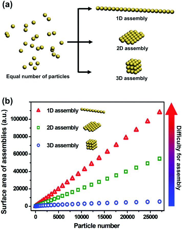 | ||
| Fig. 1 Increased surface energy of NP assemblies from 3D to 1D. (a) Schematic illustration of 3D, 2D and 1D assembly models by using the same number of NPs. (b) The dependence of surface area of different assembly models on the number of NPs. 1D assemblies (red dots) exhibit considerably larger surface area than their 2D (green dots) or 3D (blue dots) counterparts, indicating a higher difficulty in preparing such architectures. | ||
Despite their fabrication difficulty, 1D assembly of functional NPs exhibits many collective properties compared with NPs’ 2D and 3D assemblies. NPs’ 1D assembly can directionally transport excitons, photons or phonons, and shows considerable applications in waveguiding, highly sensitive sensors, microcircuits, logic computations, biomedicine, etc.3–8 In addition, the unique features of 1D assembly of NPs can bridge NPs’ fabrications with the practical devices. Therefore, there is increasing interest in controlling 1D spatial distribution of nanoscaled building blocks. Since the review given by Tang et al. in 2005,3 new advances in both fundamental research and device application have been reported, including some unusual and interesting assembly strategies in the very recent decade. Thus, it is a good opportunity to summarize and give a new review to young readers who are new to this field.
Owing to the existence of an energy barrier from 3D to 1D assemblies of NPs (Fig. 2a), providing extra energy input to overcome the barrier has been proved to be an effective strategy for controlling 1D assembly of NPs. Therefore, different routes have been explored to fabricate NPs’ 1D assemblies, which can be divided into three categories: extra energy input provided by (1) inter-particle interactions,9–12 (2) external-field forces13–17 and (3) spatial confinement strategies4,5,18–27 (Fig. 2b–d). These approaches have been successfully utilized to fabricate 1D assemblies of NPs. However, preparing such 1D structures with precise arrangement and on-demand position still remains a challenge, which is closely related to their properties and further practical applications. Luckily, some methods with a good capability of controlling NPs’1D assembly have been developed recently, e.g., field-assisted assembly,15 1D biomolecule-templated methods,22 and liquid bridge induced assembly (LBIA) strategy,5 which show promising applications in high-sensitivity sensors, colour displays and some high performance waveguiding circuits.
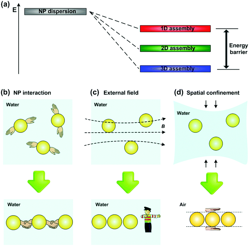 | ||
| Fig. 2 Extra energy should be applied to overcome the barrier for achieving 1D assembly of NPs. (a) Schematic illustration of the energy statuses of dispersive (grey), 1D (red), 2D (green) and 3D (blue) assemblies of NPs. The amount of NPs is the same in all cases. Owing to the existence of energy barrier from 3D to 1D assemblies of NPs, extra energy should be input by using (b) inter-particle interaction, (c) external field and (d) spatial confinement strategies for the fabrication of NP 1D assembly. | ||
The aim of this Tutorial Review is to discuss how to organize NPs into 1D assembly, and provides an easy-to-understand starting point for junior researchers who just begin to work on the field of NPs’ assemblies. We first introduce the general mechanisms to guide NPs to assemble in one direction. Subsequent to the introduction, a systematic review of diverse strategies for achieving 1D assembly of NPs will be presented, followed by a brief discussion on their advantages and challenges in each section. As this is a Tutorial Review on 1D assembly of NPs, 1D assemblies of nanowires and nanotubes, rather than NPs, will thus not be included in the present review. Meanwhile, the focused ion beam (FIB) approach that cut metallic wires into NP chains is not discussed in this review since it is a top-down technique instead of a bottom-up method. In addition, many related work will unfortunately not be included in this review due to a strictly restricted number of references. Then, we discuss some representative examples that illustrate the applications of NP 1D assemblies in optics, electronics and magnetics. Finally, we will give a brief conclusion and outlook.
2. Strategies to achieve 1D assembly of NPs
As we have discussed in the introduction part, extra energy input for NPs’ 1D assembly can be provided by inter-particle interactions, external-field forces or spatial confinement strategies (Fig. 2b–d). In this section, we will discuss the working mechanisms, species of NPs, and final appearances of 1D assembly in each approach. Challenges and advantages in technical details will be mainly focused since they highly relate to further device fabrication.2.1 Inter-particle interactions
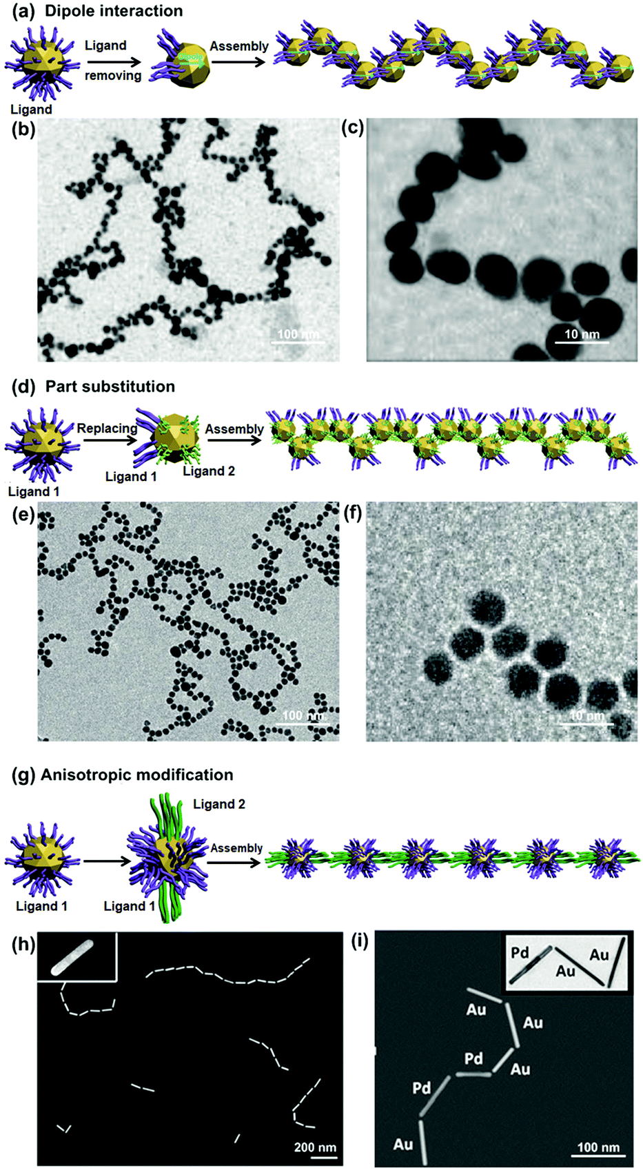 | ||
| Fig. 3 Inter-particle interaction strategies for NP 1D assembly. Schematic illustrations of dipole–dipole interaction methods by (a) removal and (d) partial exchange of ligand molecules outside NPs, and (g) molecular interaction method. (b), (e), (h) and (i) are representative transmission electron microscopy (TEM) images of branching NP 1D assemblies according to (a), (d) and (g), respectively. (c) and (f) are magnified images of (b) and (e), respectively. (b) and (c) Are reproduced from ref. 11 with permission from the American Chemical Society, copyright 2007; (e) and (f) are reproduced from ref. 9 with permission from Wiley-VCH Verlag GmbH & Co., copyright 2005; (h) and (i) are reproduced from ref. 10 with permission from Wiley-VCH Verlag GmbH & Co., copyright 2014. | ||
Removal of charged ligand molecules outside NPs can effectively reduce the repulsive interaction between NPs and generate a relatively increased dipole–dipole attraction for their 1D assembly.11,28 Mandal et al. applied such a strategy to assemble gold nanoparticles (GNPs) into 1D chains.11 The GNP surfaces were first coated with carboxylated peptide molecules through the N-terminus amino groups, and stably dispersed in solution. By adding Hg2+ ions into the solution, most of the peptide molecules were detached from the GNP surfaces due to the strong interaction between the amino groups of the peptides and Hg2+ ions. The removal of most peptide molecules from NP surfaces obviously reduced electrostatic repulsion between GNPs, and at the same time, generated an inhomogeneity of charge and polarity on GNPs. The dipole attractive interaction was thus increased and subsequently allowed adjacent GNPs to form a dimer.9,29 As the integrative dipole moment of the dimer had stronger attractive force at the end than that between NPs, other free GNPs preferentially attached to the ends of the dimer. In this way, GNPs’ 1D assembly was gradually formed (Fig. 3b and c).29
Alternatively, electric dipole–dipole interaction can be increased by partial exchange of capping charged ligands with other neutral molecules (Fig. 3d). In this way, NP surfaces exhibit a non-uniform spatial distribution of charge and polarity, allowing for 1D assembly of NPs through the dipole–dipole interaction. This idea has been developed by Mann et al. to assemble GNPs into 1D architectures.9 At the beginning, GNP surfaces were protected by citrate ligands, which had been partially substituted by mercaptoethyl alcohol (MEA) molecules. After partial substitution of the capping ligands, the surfaces of GNPs were covered with mixed ligands, resulting in reduced electrostatic repulsion and increased dipole–dipole interaction. The extent of surface ligand exchange could be finely controlled by the MEA/GNP molar ratio. In a proper ratio range, e.g., between 3000:1 and 10000:1, the dipole–dipole interaction was strong enough to overcome the repulsion force between NPs, yielding GNP 1D assembly (Fig. 3e and f). The length of NP chains could reach up to several micrometers.
The anisotropic shape of NPs can also influence the directional assembly of NPs. The non-spherical shapes result in anisotropic electric polarizabilities, which may further affect the directional interactions between NPs and thus the 1D assembly. The interested readers are referred to the work by Glotzer et al.30
Based on this selective adsorption mechanism, Kumacheva et al. have demonstrated the 1D assembly of metallic nanorods (NRs) (e.g., gold and platinum) by using a two-step ligand modification strategy to introduce directional interactions between NRs (Fig. 3g).10,12 The gold NRs were side-coated with CTAB molecules and end-functionalized with thiol-terminated polystyrene (PS, MW 12000 g mol−1) due to different binding abilities of these two molecules on the gold crystal facets. Upon addition of a certain amount of water to the gold NR dispersion in dimethylformamide (DMF), gold NRs would undergo end-to-end assembly into 1D structures due to the PS attractive interactions. The NR chain growth process is similar to the molecular polymerization approach, and is also called colloidal polymerization. Finally, they were able to align gold NRs with different lengths (Fig. 3h), and co-assembled gold and platinum NRs to form a composite 1D structure (Fig. 3i).10
2.2 External field-induction
It should be pointed out that inter-particle interaction strategies, no matter driven by electric-dipole or molecular interaction, are difficult to precisely control the arrangement of NPs along one direction. The spatial distribution of charge and/or polarity on the NP surfaces after diverse chemical treatment is uncontrollable, and the linker agents are usually flexible in molecular structure, both of which contributing to the random attachment of NPs to each other. As a consequence, branching and interconnectivity structures of NP chains are inevitably formed.Assembly of NPs under external fields can be achieved with a combination of speed and precision. An applied external field can allow each dispersed NP suffering a driving force in the same direction. Owing to the existence of the unidirectional force upon each NP surface, dispersive NPs will preferentially attach to each other along the direction of the driving force. External fields provide not only a directional driving force, but also an extra energy input to overcome the energy barrier, leading to the controlled formation of a regular NP 1D assembly.
Most recently, an electric field was combined with the capillary effect to flexibly align conductive particles into 1D chains in a single particle width, as well as controlled patterns.15 As shown in Fig. 4a, silver-coated hollow silica microparticles (diameters from 100 nm to 200 μm) were dispersed in silicon oil. Then, a high-frequency alternating current (AC) electric field (20 kHz, square wave) was applied through a tip electrode to the surface of the dispersion (Fig. 4a, left). The conductive particles near the external field were polarized, and subsequently moved towards the tip of the electrode. When the electrode was raised, the particles connected by a liquid bridge were sequentially pulled out from the liquid only if the dielectrophoresis force exerted on the particle was larger than the downward capillary force. In this way, a chain as long as several centimeters was obtained. Once the chain was formed, the structure remained even after the removal of the electric field (Fig. 4b). In addition, the stable and flexible particle chains were easy to construct in different shapes by direct writing, indicating the potential for generating particle electronic circuits.
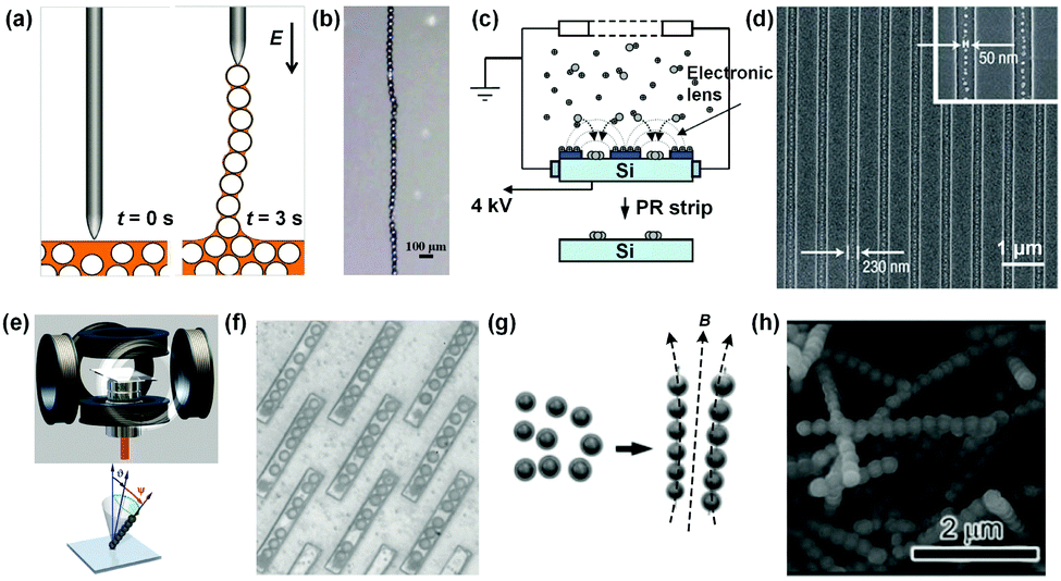 | ||
| Fig. 4 External field-induction strategies for NP 1D assemblies. Schematic illustrations of electric field induced methods for 1D assemblies of (a) microparticles and (c) nanoparticles. (b) and (d) are the representative photograph and scanning electron microscopy (SEM) image of particle 1D assemblies according to (a) and (c), respectively. (e) Schematic illustration of the magnetic field induced method for NP 1D assembly. A homogeneous magnetic field with designed direction and varying magnitude was produced and integrated into an optical microscope. (f) Representative photograph of 1D assembled magnetic microparticle arrays controlled by an external magnetic field. The trenches ensured that all chains had approximate length and width. (g) Schematic illustration of the pre-treatment method to solve the breaking problem of formed NP 1D structures after the removal of the external field. Superparamagnetic Fe3O4 colloidal nanocrystals were coated with a thin layer of silica precursor to form a mechanically robust shield for retaining the structure of NP 1D assembly. (h) SEM image of a firm NP 1D assembly. (a) and (b) Are reproduced from ref. 15 with permission from the Nature Publishing Group, copyright 2017; (c) and (d) are reproduced from ref. 16 with permission from the Nature Publishing Group, copyright 2006; (e) and (f) are reproduced from ref. 17 with permission from the American Association for the Advancement of Science (AAAS), copyright 2010; (g) and (h) are reproduced from ref. 13 with permission from the Wiley-VCH Verlag GmbH & Co., copyright 2011. | ||
An electric field could also be used to prepare NP 1D structures over large areas and with an ultra-high resolution, which is important for the integration of nanodevices. A typical example is shown in Fig. 4c. A mixture of positively charged aerosol silver NPs (SNPs; 10 nm) and positive nitrogen ion gas generated by the corona discharger was fed together into an electrostatic precipitator (ESP) chamber (Fig. 4c).16 Under the applied electric field between the chamber and the pre-patterned photoresist (PR) substrate, charged ions deposited on the PR surface. The charge accumulated on the PR surface distorted the initially equipotential planes into convex planes, which then acted as nanoscopic electrostatic lenses around the PR patterns and directed charged SNPs to assemble in 1D patterns. Finally, well formed 1D structures of SNPs were obtained (Fig. 4d). This method is versatile and can be applied to any NPs which can be aerosolized. It is worth noting that the SNPs are not connected with each other because of the electrostatic repulsion between them in the deposition process, which may negatively influence the electrical or photonic properties of the as-prepared structures.
Vilfan et al. reported a typical assembly of superparamagnetic NPs (Dynabeads Epoxy M-450; 4.4 μm) into 1D arrays by applying an external magnetic field.17 As shown in Fig. 4e, three orthogonal pairs of coils were constructed to generate a homogeneous magnetic field. The magnetic field direction and strength were tunable. By applying the external field, magnetic dipole moments induced in the superparamagnetic particles were aligned parallel to the direction of the external magnetic field. Subsequently, the magnetic-dipole attraction between the particles led to the formation of 1D colloidal chains. The actuation of the chains could be tuned by tailoring the magnetic field direction. In order to control the length of the chains, trenches in a PR surface were used, allowing for regular 1D assembly of particles (Fig. 4f).
Generally, the obtained 1D structures composed of superparamagnetic NPs would dissociate after the removal of the applied magnetic field, due to the loss of induced magnetic dipoles. Yin et al. proposed a solution by coating the NP 1D assembly with a thin layer of silica (Fig. 4g).13 Superparamagnetic Fe3O4 colloidal nanocrystals were first coated with a thin layer of silica precursor after the synthesis, and then guided to assemble along one direction by an applied magnetic field. During the formation of NP chains, the silica precursor layer outside NPs would connect neighboring NPs. Continued deposition of silica finally resulted in a mechanically robust coating to retain the structure of NP 1D assembly (Fig. 4h).
2.3 Spatial confinement
The spatial confinement strategy is direct and easy to understand. Spatial restriction, from no matter hard templates, soft organic micelles or water stripes, can be used to force 1D assembly of NPs (Fig. 2d). Extra energy input has been provided by this confined space to organize NPs in a row. Pending on the types of confined space, currently reported approaches can be divided into two categories: fixed space and shrinking space.(a) Hard 1D templates. 1D fixed spaces, provided by porous alumina,18 carbon nanotubes (CNTs),20 boron nitride nanotubes,38 ridge-and-valley structures,19 or grooved modified PDMS or PMMA templates,21 can restrict NPs to organize in one direction, and are popularly used for directing 1D assembly of NPs. Since this strategy just utilizes the confined space effect, special requirements of NPs, such as conductivity in the electrical field method15,16 or superparamagnetivity in the magnetic field approach,13,17 are not necessary, indicating wide adaptation of this strategy.
Porous alumina templates have been widely employed from fundamental research to diverse applications due to their linearly aligned pore structures with tunable pore size and simple preparation process. Their linear channels provide ideal spaces for 1D assembly of NPs when they were filled with the NP dispersion by using selective methods, e.g., vacuum induction, electrophoretical procedure or capillary-dipping methods (Fig. 5a). For example, gold clusters with a diameter of ca. 4.2 nm could be electrophoretically filled into the alumina nanochannels with a diameter of ca. 7 nm. Owing to the physically confined space effect, the gold clusters formed strictly aligned chains inside the channel, as shown in the TEM result (Fig. 5b).18
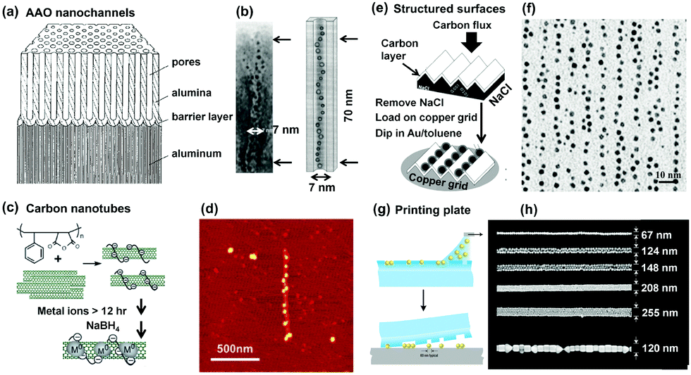 | ||
| Fig. 5 Hard templates provide fixed 1D space for guiding 1D assembly of NPs. Schematic illustrations of 1D confined space, provided by (a) porous alumina, (c) carbon nanotubes, (e) ridge-and-valley structure and (g) grooved PDMS templates, to physically restrict NPs to stand in one direction. Representative (b) TEM, (d) atomic force microscopy (AFM), (f) TEM and (h) SEM images of as-prepared NP 1D assemblies by using (a), (c), (e) and (g) methods, respectively. (a) and (b) Are reproduced from ref. 18 with permission from the Royal Society of Chemistry, copyright 1997; (c) and (d) are reproduced from ref. 20 with permission from the American Chemical Society, copyright 2006; (e) and (f) are reproduced from ref. 19 with permission from the American Chemical Society, copyright 2002; (g) and (h) are reproduced from ref. 21 with permission from the Nature Publishing Group, copyright 2007. | ||
Carbon nanotubes (CNTs) have attracted great research interest due to their promising physical properties and potential applications in electronics and optics. Furthermore, their linear geometry makes them useful as structure-directing matrices for the preparation of 1D assemblies of NPs. Considerable hardness and toughness of CNTs allow them to maintain their shapes and structures intact. As a result, both the outside surface and inside cavity of CNTs can be used to direct the assembly of NPs. In order to guide 1D assembly of NPs, certain surfactants are usually used in this method for two reasons. The organic surfactant molecules not only make CNTs soluble in aqueous solutions but also enable NPs to bind onto the CNT surfaces. In Chen's report,20 poly(styrene-alt-maleic acid) (PSMA) surfactant was employed to disperse CNTs in the solution, as well as the binding of metal ions through electrostatic interactions (Fig. 5c). The benzene groups of PSMA interacted with CNTs by hydrophobic interactions while the charged backbones of PSMA promoted the dispersion of CNTs in water. The later reduction of captured metal ions led to the generation of NPs (e.g., Pt). Thus, 1D assembly of NPs could be found along one CNT structure, as shown in Fig. 5d.
A ridge-and-valley structured carbon film can also be used to form 1D arrays of NPs. The interchain distance is tunable by selecting different inorganic crystals to act as faceted templates. As a typical example illustrated in Fig. 5e, NaCl crystals were selected as the templates to form ridge-and-valley structures. Subsequently, a carbon film with the ridge-and-valley structure was obtained by directly depositing a thin film of carbon onto the NaCl surface, which could be used to direct the formation of 1D arrays of GNPs by dipping the carbon film into a gold solution (Fig. 5f).19
Another important category of 1D hard templates is the solid surfaces with 1D chemically modified patterns or physically etched geometries, which are usually fabricated via lithography techniques, e-beam or nanoimprinting. These methods have been significantly developed in the past decades for ordering NPs into 1D assembly. The features of the resulting 1D geometries can be precisely and reproducibly created in the range of tens of nanometers to the macroscopic scale. The alignment of NPs in the confined 1D space is thus associated with the parameters of the templates, including height, width, and length. Wolf et al. demonstrated such an example, as shown in Fig. 5g.21 A PDMS template with defined linear structures was obtained by soft lithography. Then, GNPs in an aqueous solution were directly deposited into the topographical features of the template with predefined wetting properties. The obtained 1D arrays of GNPs could be stored in the polymeric template and transferred onto substrates when needed. Fig. 5h shows as-prepared 1D arrays of GNPs with different widths on a silicon substrate.
For 1D hard templates, it's able to preserve the well-defined structure shapes and keep the structure intact, even in harsh environments. In addition, advances in lithography have enabled the production of reproducible patterning of features on a template in a wide range of sizes and over large areas, which is thus beneficial for controlled 1D assembly of NPs. Then, GNPs in an aqueous solution were directly deposited into the topographical features of the template with predefined wetting properties. The obtained 1D arrays of GNPs could be stored in the polymeric template and transferred onto substrates when needed. Fig. 5h shows as-prepared 1D arrays of GNPs with different widths on a silicon substrate.
(b) Soft templates. Besides artificial 1D hard templates, many biomolecules, such as viruses,39 DNA,4,22 polysaccharides,40 proteins or peptides,24,25 are also utilized to dictate the 1D organization of NPs. Inspired by the nature's concept, synthesized soft templates by co-polymers23 and surfactant molecules41 have also been exploited.
Protein nanotubes assembled from ring-shaped proteins can serve as ductile scaffolds in which NPs arrange to form 1D structures. For example, 2-Cys peroxiredoxins (Prxs) are abundant cellular ring proteins, which can assemble into a short nanotube structure after a sequential treatment of oxidation, reduction, and stress conditions (e.g., oxidative, acidic and thermal). Ippoliti and Angelucci et al.25 reported a method to obtain stable and high-aspect ratio protein nanotubes by using the protein SmPrxI (i.e., 2-Cys peroxiredoxin I from the human parasite Schistosoma mansoni) in the presence of divalent metallic ions, such as Ni2+, Zn2+, and Co2+ (Fig. 6a). The selective interaction between N-terminal regions of the protein and such metallic ions is the key to build such tube structures. Based on this mechanism, GNPs attached by Ni2+ ions on their surfaces can be restricted inside the protein tubes, forming a straight chain of GNPs (Fig. 6b).
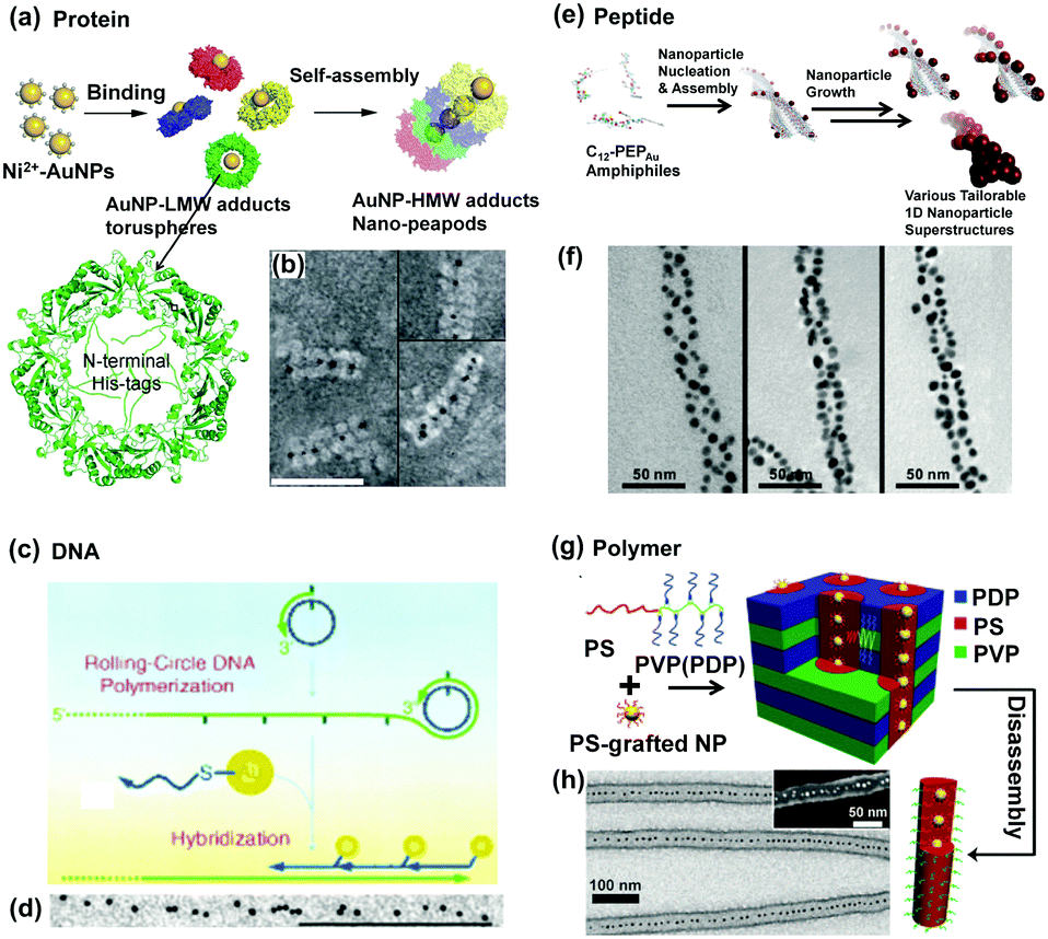 | ||
| Fig. 6 Soft templates provide fixed 1D space for guiding 1D assembly of NPs. Schematic illustrations of 1D confined space, provided by (a) protein formed nanotubes, (c) DNA complementary strands, (e) double helix peptide structure and (g) chemically synthesized block copolymers, to physically restrict NPs to stand in one direction. (b), (d), (f), (h) are representative TEM images of as-prepared NP 1D assemblies according to (a), (c), (e) and (g) methods, respectively. (a) and (b) Are reproduced from ref. 25 with permission from the Royal Society of Chemistry, copyright 2014; (c) and (d) are reproduced from ref. 22 with permission from Wiley-VCH Verlag GmbH & Co., copyright 2005; (e) and (f) are reproduced from ref. 24 with permission from the American Chemical Society, copyright 2010; (g) and (h) are reproduced from ref. 23 with permission from Wiley-VCH Verlag GmbH & Co., copyright 2011. | ||
DNA is probably the most frequently used biomolecule which can act as a template for NP assembly due to its specific molecular recognition property. There are two typical interactions directing the successful 1D assembly of NPs. One is the electrostatic attraction between charged NPs and DNA templates.4 The other one is based on the hybridization between one DNA template and another complementary DNA strand attached to NPs. The latter one was first demonstrated by Mao et al.22 as shown in Fig. 6c. GNPs with a diameter of ca. 5 nm were functionalized with DNA1 molecules. Then, such GNPs could assemble along another DNA strand template which owns a large number of repeats complementary to DNA1 via DNA hybridization. In this way, 1D assembly of GNPs with the length of several microns could be generated, which was obviously found in the TEM observation (Fig. 6d).
Peptide molecules are another linear biomolecules which can act as structural templates for directing NP organization via electrostatic interaction between NPs and charged groups of peptides. It's interesting that 1D helical structural assembly of GNPs can be obtained using peptide as a template.24 As shown in Fig. 6e, specific peptide sequences (C12-PEPAu) were bonded with GNP seeds, and self-assembled into double helix templates, leaving the GNP seeds outwards. Following the crystallization growth of GNP seeds, well-organized double helices of GNPs were finally obtained. The interhelical distance of the GNP 1D assembly could be tuned by using different capping agents (Fig. 6f).
Inspired by nature, chemically synthesized block copolymers can also be used to assemble into cylindrical or wormlike micelle structures, providing confined spaces inside to guide 1D assembly of NPs with controlled particle position and orientation. The incorporation of NPs into assembled polymer micelles can be achieved via electrostatic or hydrophobic interaction between the polymer moieties and NPs. In one example here,23 polystyrene–poly(4-vinylpyridine) (PS20k–P4VP17k, volume fraction of PS ΦPS = 56%) was first dissolved with pentadecylphenol (PDP) in chloroform to form comb-coil supermolecules PS–P4VP(PDP)x (x represents the ratio of PDP to 4VP units). Further addition of PS2k-coated GNPs into the system would generate hierarchical structures, as shown in Fig. 6g. The GNPs were selectively encapsulated inside the cylindrical PS via hydrophobic interactions between GNPs and the PS block of PS–P4VP(PDP)x. As a result, 1D assembly of GNPs could be obtained after removal of the PDP molecules (Fig. 6h).
As soft templates for NP 1D assembly, biomolecules (e.g., proteins, DNA molecules, or viruses) are attractive, which can be attributed to their distinct chemical structures and the exceptional selectivity of the biomolecular assembly. In addition, biomolecules provide multiple well-defined binding sites for directing the assembly of NPs. With respect to synthetic molecules, the superior advantage is that their composite and molecular structure can be specifically tailored to match target NPs, and thus achieve a particular 1D structure.
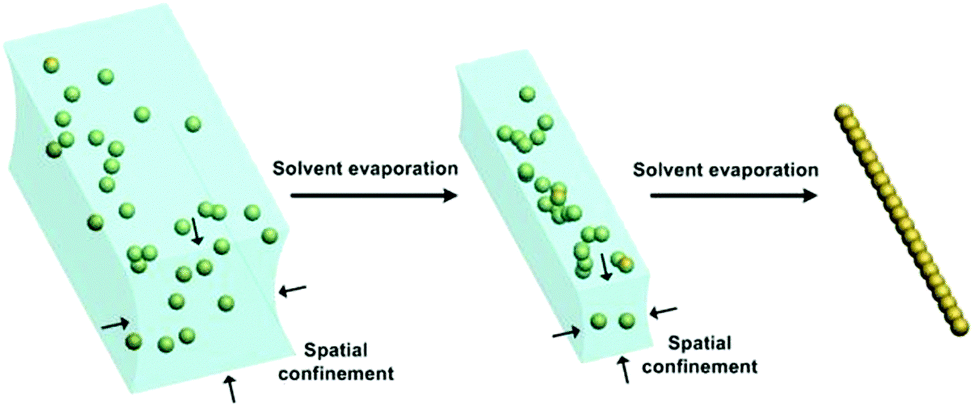 | ||
| Fig. 7 Water stripe can provide shrinking 1D spaces to facilitate the 1D assembly of NPs. Schematic illustration of water-templated NP 1D assembly. NPs are first dispersed in a water stripe. With the evaporation of water, the water stripe will shrink inwards, leading to increased surface tension for restricting the alignment of NPs. Finally, ordered 1D assembly of NPs can be formed while the water template disappears without any residue. | ||
Very recently, this water-templated 1D assembly of NPs was directly observed by Mirsaidov et al. through in situ liquid-cell transmission electron microscopy (LC-TEM).42 The experimental platform is schematically shown in Fig. 8a. GNP solution was sandwiched between two translucent SiNx films. In particular, the bottom SiNx film was fabricated with a microchannel structure while the top one was flat (Fig. 8b). Based on this special cell design, the stepwise self-assembly dynamics of hydrophobic GNPs into 1D assembly can be directly observed (Fig. 8c). First, a meniscus of water stripe formed between neighbouring nanochannel walls. With the slow evaporation of water, GNPs gradually accumulated in the middle part of the water stripe. Owing to the strong van der Waals attraction between the ligands outside particle surfaces, dispersive nanoparticles were closely packed along the water stripe direction, yielding 1D assemblies of GNPs in the centers of the nanochannels (Fig. 8d). Thereby, water stripes can provide 1D shrinkable spaces to facilitate the 1D assembly of NPs. Then, two questions have been raised: how to generate the liquid stripes? And how to make use of them?
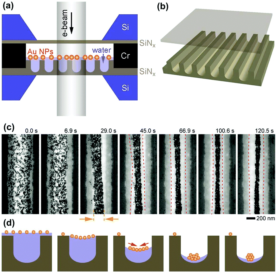 | ||
| Fig. 8 In situ TEM observation of the formation of 1D assembly of NPs driven by shrinking space inside evaporated water stripes. (a and b) Schematic illustrations of the experimental setup. A solution of hydrophobic GNPs was encapsulated between a nanochannel-structured silicon nitride (SiNx) and a top flat one. (c) In situ TEM image series showing the process of NP 1D assembly following the evaporation of water. (d) Schematic illustrations of the cross-sectional parts according to (c), respectively. (a–c) Are reproduced from ref. 42 with permission from Wiley-VCH Verlag GmbH & Co., copyright 2017. | ||
Generally, a liquid is inclined to form a spherical shape due to the minimization of surface energy. The generation of linear liquid stripes indicates extra increase of surface energy, requiring some creative strategies to meet this challenge. For example, Yang et al. reported a dip-coating method to generate parallel arrangements of water stripes upon a flat substrate.27 1D assemblies of NPs were fabricated following gradual shrinking of such confined water stripes. As shown in Fig. 9a, a flat substrate vertical to the NP solution was slowly pulled out of the liquid with a colloidal Langmuir–Blodgett (LB) monolayer. NPs at the water–substrate interface were carried off the water surface and deposited onto the substrate, allowing for the generation of separated NP domains after the water evaporation (Fig. 9b). As the substrate was continuously pulled out of the solution, more NPs would assemble along the pulling direction, yielding 1D assembly arrays driven by the capillary force of water stripes (Fig. 9c).
 | ||
| Fig. 9 Liquid stripe templates provide 1D shrinkable spaces for guiding 1D assembly of NPs. Schematic illustrations of 1D shrinkable spaces, generated by (a) a dipping-coating method and (d) an unsymmetrical geometry induced approach, to physically restrict NPs to assemble in one direction. Representative (b and c) dark-field photographs and (e and f) SEM images of as-prepared NP 1D assemblies corresponding to (a) and (d) methods, respectively. (a–c) are reproduced from ref. 27 with permission from the Nature Publishing Group, copyright 2005; (d–f) are reproduced from ref. 26 with permission from Wiley-VCH Verlag GmbH & Co., copyright 2012. | ||
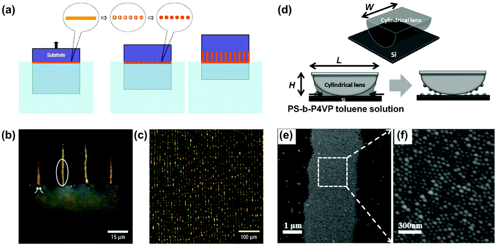
Alternatively, Lin et al. demonstrated another strategy to generate liquid stripe arrays by sandwiching the poly(styrene)-block-poly(4-vinylpyridine) (PS-b-P4VP) toluene solution between a cylindrical lens and a flat silicon substrate (Fig. 9d).26 With the evaporation of toluene, as well as an unsymmetrical geometrical structure of the setup, the organic liquid would pin upon the substrate then suddenly break, leaving a parallel arrangement of liquid stripes. The organic liquid slowly moved toward the cylinder following the evaporation of toluene, generating a series of 1D structures composed of PS-b-P4VP micelle particles, as shown in Fig. 9e and f.
In most recent years, a new method named liquid bridge induced assembly (LBIA) has been rapidly developed and actively employed to flexibly prepare 1D assembled structures of NPs.43 The basic mechanism is to control the dewetting of liquids upon the solid surfaces. At the molecular level, the top atomic/molecular layer of the lyophilic areas attracts the liquid molecules while those in the lyophobic regions will repel the liquid molecules to other places. Accordingly, the dewetting of liquid can move from the lyophobic (low-surface-free-energy) area towards the lyophilic (high-surface-free-energy) region. When introducing regular lyophilic domains onto a lyophobic surface, highly ordered liquid stripes (i.e., liquid bridges) with several micrometers in width can be attained between the lyophilic domains.43 Each microscaled liquid stripe provides a linearly confined space for the assembly of NPs inside the liquid, leading to ordered 1D assemblies of functional materials. With a carful design of lyophilic/lyophobic domains on the substrate, the pattern of the micro-scaled liquid bridges, including the location, orientation and density, can be controlled to be formed, thus resulting in desired 1D assemblies of NPs.
As a typical example shown in Fig. 10a, a drop of GNPs or SNPs was sandwiched between a desired flat cover slide and a superhydrophilic silicon wafer substrate with spindle-shaped pillar structures.44 With the evaporation of water, micropillar arrays acted as wetting defects to induce regular rupture of NP solution, yielding ordered liquid stripes bridging neighboring micropillars (Fig. 10b). Microscaled water stripe shrunk inwards, leading to increased surface tension for restricting the alignment of NPs. Finally, ordered 1D assembly of NPs can be formed upon the desired substrate. The whole process of liquid stripe formation and 1D assembly of NPs was clearly recorded by snapshots of a video, as shown in Fig. 10c.
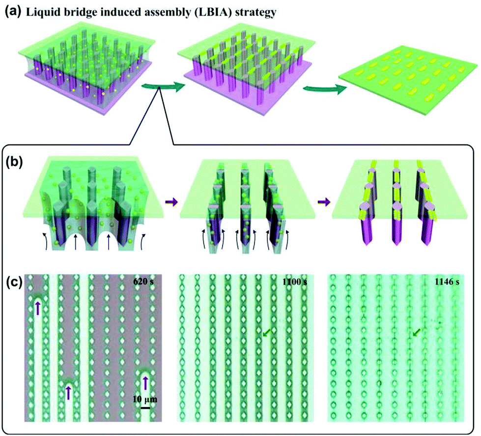 | ||
| Fig. 10 Liquid bridge induced assembly (LBIA) strategy provides regularly and precisely positioning water stripe templates to generate programmed NP 1D assembly. (a) Schematic illustrations of LBIA strategy. NP suspension was sandwiched between a spindle-pillar-structured template and a flat substrate. With the evaporation of solvent, the micropillar array served as wetting defects to control the rupture of NP solution, yielding micrometer-scaled liquid bridges between neighboring micropillars. An array of close-packed, linear assemblies of NPs could be formed upon the desired substrate. After removal of the pillar-structured template by physical peeling, a precisely positioned NP 1D assembly pattern can be generated accordingly. (b) Schematic illustration shows formation details of liquid bridge and final NP 1D assembly. These liquid bridges provide gradually reducing confined spaces for SNP aggregation, yielding a linear arrangement of SNPs upon the desired substrate. (c) Snapshots of a video recording shows the in site observation of the formation of SNP 1D assemblies. (a–c) Are reproduced from ref. 44 with permission from Wiley-VCH Verlag GmbH & Co., copyright 2014. | ||
The LBIA strategy can easily tailor the width of NP 1D assembly, and is widely adapted to different species of NPs. Since the occupation probability of each NP is the same in the LBIA process, high concentrated NP suspension leads to wider 1D structures, while diluted NP solution will result in narrow, even single particle-wide, linear architectures. Taking the GNPs as an example,5 the GNPs with diameter of ∼45 nm were mixed with calcein and assembled upon pillar-structured substrates. Ordered zigzag-type GNP assemblies could be prepared, whose widths were tunable ranging from 6–8 GNPs to single GNP (Fig. 11a–f). Soon after that, we used a grooved substrate to guide the assembly of SNPs.44 A 1D architecture with single-particle width was achieved by carefully tailoring the concentration of the SNP suspension (Fig. 11g). The particle size in the LBIA can range from several nanometers, such as quantum dots (Fig. 11h), to hundreds of nanometers, like polystyrene (PS) microspheres (Fig. 11j). Wide particle size distribution of commercial TiO2 does not affect the performance of the LBIA process (Fig. 11i). However, narrower distribution of particle size could yield more ordered arrangement of particles (see Fig. 11j). Magnetic ferriferous oxide NPs can also be aligned in one direction by the LBIA strategy without the assistance of an external magnetic field (Fig. 11k).45
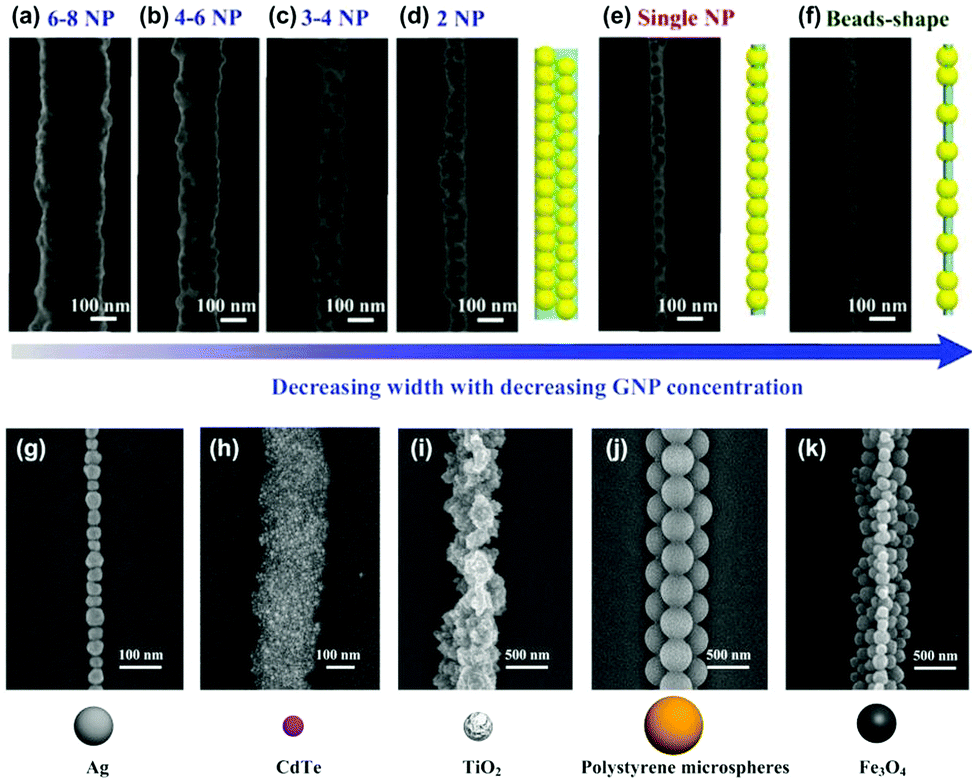 | ||
| Fig. 11 The LBIA strategy can tune the width of NP 1D assembly and is widely adapted to different species of NPs. TEM images of GNP 1D assemblies with tunable widths from (a) 6-8, (b) 4-6, (c) 3-4, (d) 2 to (e) single particle size by decreasing the GNP/calcein ratio. (f) A bead-shaped GNP necklace can also be generated. SEM images of (g) SNPs, (h) CdTe quantum dots, (i) commercially irregular TiO2 grains, (j) polystyrene NPs and (f) magnetic Fe3O4 NPs that are assembled into 1D structures by the LBIA strategy. (a–f) Are reproduced from ref. 5 with permission from Wiley-VCH Verlag GmbH & Co., copyright 2013; (g–j) are reproduced from ref. 44 with permission from Wiley-VCH Verlag GmbH & Co., copyright 2014; (k) is reproduced from ref. 45 with permission from Wiley-VCH Verlag GmbH & Co., copyright 2016. | ||
The geometric shapes and the locations of hydrophilic domains can be tailored to effectively govern the patterning of NP 1D assemblies in the LBIA strategy.46 Taking the SNP linear patterning as an example, “T”, “Y” and “V” shaped NP 1D assemblies can be obtained by carefully designing the pillar shapes and locating them in the pre-designed position (Fig. 12a–e).
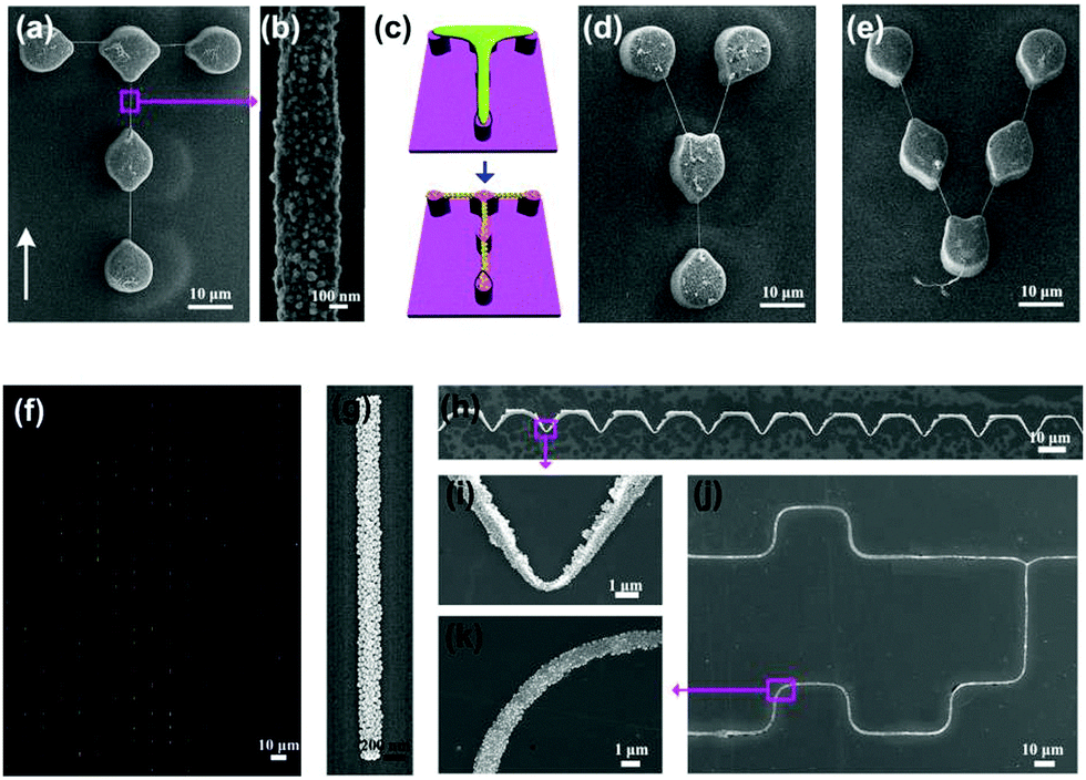 | ||
| Fig. 12 On-demand patterning of NP 1D assemblies by tailoring the geometric shapes and the locations of lyophilic domains in the LBIA strategy. SEM images of (a) “T”, (d) “Y” and (e) “V” shaped NP 1D assemblies. (b) Is a magnified image of (a). (c) Schematic illustration of the formation process of “T” shaped NP 1D assembly. Representative images of (f) linear, (h) undulating shaped and (j) complex GNP 1D assemblies. (g), (i) and (k) are magnified images of (f), (h), (j), respectively, exhibiting advanced ability of the LBIA strategy to precisely position the NP 1D assembly. (a–e) Are reproduced from ref. 46 with permission from Wiley-VCH Verlag GmbH & Co., copyright 2014; (f–j) are reproduced from ref. 44 with permission from Wiley-VCH Verlag GmbH & Co., copyright 2014. | ||
The length of liquid stripes introduced by micropillars is limited, commonly tens of micrometers depending on the design of pillar-structured substrates, which directly restricts the length of NP 1D assembly and related application. To solve this problem, separated micropillars (Fig. 12f and g) were upgraded into continuous tooth-shaped or more complex grooves.44 Through a selective modification of microgrooves, the groove tops showed a lyophobic property while their side walls exhibited a lyophilic behavior. Therefore, the dewetting of liquid was restricted inside the groove gaps, producing on-demand NP circuits at the edges of each microgroove (Fig. 12h–j), which is promising for fabricating complex circuits.
3. Applications
The applications of NPs’ 1D assembly strongly depend on their material properties, particle size, shapes and interparticle distance. Metallic and semi-conductive NP chains (e.g., SNPs, GNPs, and SnO2 NPs) present remarkably different optical and/or electric properties while 1D assembly of superparamagnetic NPs (e.g., Fe3O4) exhibits interesting collective magnetic properties, in comparison with their bulk materials or discrete NPs. These unique properties of NPs’ 1D assembly originate from the coupling of the surface plasmons, excitons or magnetic dipoles, and have shown exciting progress in the past few decades. In addition, the increasing requirement for miniaturization of optoelectronic devices requires more convenient and cost-effective methods for device fabrication and integration. The unique feature of NP 1D assembly can bridge NPs’ fabrications with their practical devices. Specifically, the assembled geometry and structure quality have a significant impact on their properties and applications. Recently, some newly developed strategies15,21,44 could endow the NP 1D assemblies with not only regular arrangement but also precise position, which generates wide interest in the research on multiple applications of electronics, photonics, and magnetics.3.1 Electronics
1D structures composed of specific metallic or semi-conductive NPs may have quite different electrical properties from those of individual NP and corresponding bulk samples. The electron transport is significantly influenced by the particle size and geometric structure of the chains. Ben-Yoseph et al. reported that 1D assembled structure of SNPs (30–50 nm in diameter) on a DNA template between two electrodes exhibited a highly nonlinear and asymmetric I–V curve, rather than ohmic electrical characteristics. At higher bias (depending on synthesized conditions), the NP chain was conductive while a zero-current plateau developed when the voltage bias was approaching 0.4 SNP chains obtained by the LBIA method exhibited 1.5 times higher conductivity than NP lattices, which was attributed to relatively compact NP aggregations.46 The special electric properties of 1D structures are further exploited in electronic devices.Tseng et al. showed an electronic memory device with a large on/off ratio based on the conductance switching of 1D assembled platinum NPs (PNPs).39 PNP chains were prepared using tobacco mosaic virus (TMV) as templates, shown by the TEM observation in Fig. 13b. The average particle size was about 10 nm. The 1D structures were dispersed in a PVA matrix and sandwiched between aluminium electrodes (Fig. 13a). When a low voltage was applied to the electrode, the current was low. But an abrupt increase in the current (from 10−8 A to 10−5 A) occurred when the voltage was higher than 3 V, indicating a conductive state of the 1D structures (Fig. 13c). The high conductance state was stable and could be switched to the low conductance state when a reversed voltage higher than 2.4 V was applied. This interesting conductance-switching property could not be observed in control devices using only TMV, PVA or PNPs. The mechanism of this process is attributed to charge trapping in the nanoparticles for data storage and a tunnelling process in the high conductance state. They further demonstrated that this memory device based on bistable conductivity could reach about 400 cycles.
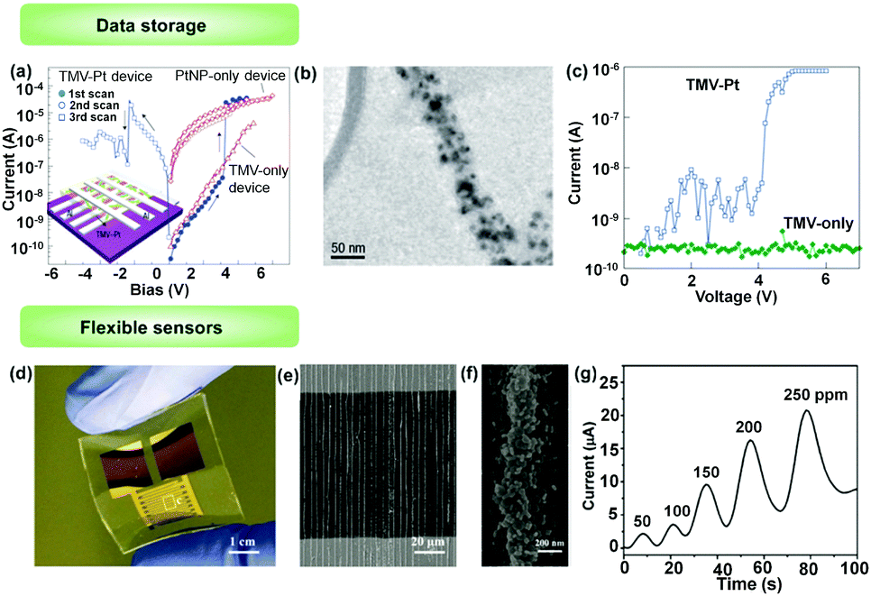 | ||
| Fig. 13 Applications of NPs’ 1D assemblies in electronics. (a) Typical room temperature I–V characteristics of the tobacco mosaic virus (TMV)–Pt device. (b) TEM image of TMV nanowire conjugated with Pt nanoparticles. (c) Typical room temperature I–V characteristics of TMV–Pt (blue line) and TMV-only configuration (green). (d) A photograph of a flexible, high-sensitive gas sensor based on 1D assembly of binary NPs. (e) SEM image of 1D assemblies of binary NPs. Two kinds of NPs, SnO2 NPs and GNPs were integrated into 1D assemblies through the LBIA strategy, bridging neighbouring electrodes. (f) is a magnified image of (g), showing the details of binary NP chains. (d) An electrical response curve of the SnO2/GNP binary gas sensor toward the exposure of acetone with different concentrations. (a–c) Are reproduced from ref. 39 with permission from the Nature Publishing Group, copyright 2006; (d–g) are reproduced from ref. 47 with permission from Wiley-VCH Verlag GmbH & Co., copyright 2017. | ||
Jiang et al.47 fabricated a flexible, high-sensitive gas sensor based on 1D assembly of binary NPs. Two kinds of NPs, SnO2 NPs and GNPs were integrated into 1D assemblies through the LBIA strategy, bridging neighbouring electrodes (Fig. 13d). Due to the size difference of binary NPs (the diameter of SnO2 NPs is three times larger than that of GNPs), GNPs were deposited upon the surfaces of SnO2 NPs, yielding several active points for gas sensing (Fig. 13e and f). The sensing performances were evaluated by measuring the change of electrical conductivity of the NP 1D assembled gas sensors. A sharp enhancement of conductivity was observed for the device using SnO2/GNP binary NP 1D assemblies when exposed to 50 ppm of acetone, compared with that by using individual SnO2 NP 1D assemblies. The peak current intensity was improved ca. 5 times in the presence of GNPs. Meanwhile, the peak current intensities were linearly related to the acetone gas concentrations. The sensitivity of binary NP sensors was increased from 2.3 μA (50 ppm) to 20.2 μA (250 ppm) (Fig. 13g).
3.2 Photonics
The optical properties of 1D assemblies of metallic NPs (e.g., GNPs, SNPs and a variety of transition metal NPs) provide a good example of collective behavior in NP assemblies, and have been well investigated from both theoretical and experimental viewpoints. Plasmonic noble metal NPs exhibit localized surface plasmon resonance (LSPR) when excited by appropriate incident light, resulting in significant resonance scattering and absorption in the visible spectrum, which is related to particle size and shape, the composition of the NPs and the dielectric environment surrounding the NPs. The frequency of LSPR can be significantly influenced when NPs are brought in close proximity and interparticle coupling occurs. For example, for the GNP chain, the longitudinal plasmon resonance will red shift compared with dispersed GNPs. In addition, the coupling interaction can generate strong optical fields confined in the space between NPs,48 which can dramatically intensify the Raman scattering and be actively used for sensing.The optical change due to the plasmonic band shift of metal NPs can be used for sensing target molecules. For example, Kotov and Xu et al. successfully applied the 1D assembly transition of GNRs for the detection of microcystin-LR (MC-LR), a pervasive environmental toxin produced by cyanobacteria.6 As shown in Fig. 14a, GNRs with selective modification of MC-LR antibodies and MC-LR-OVA antigens in the ends were prepared, respectively. The specific antibody–antigen interaction generated side-to-side assembly of GNRs, which exhibited a coupling longitudinal surface plasmon peak located at about 900 nm. In the presence of MC-LR, the 1D chain was disassembled, and the longitudinal peak shifted towards 700 nm with increased intensity depending on MC-LR concentration (Fig. 14b). This optical property change could detect MC-LR in the range of 0.05 ng ml−1 to 1 ng ml−1 with a detection limit of 0.03 ng ml−1.
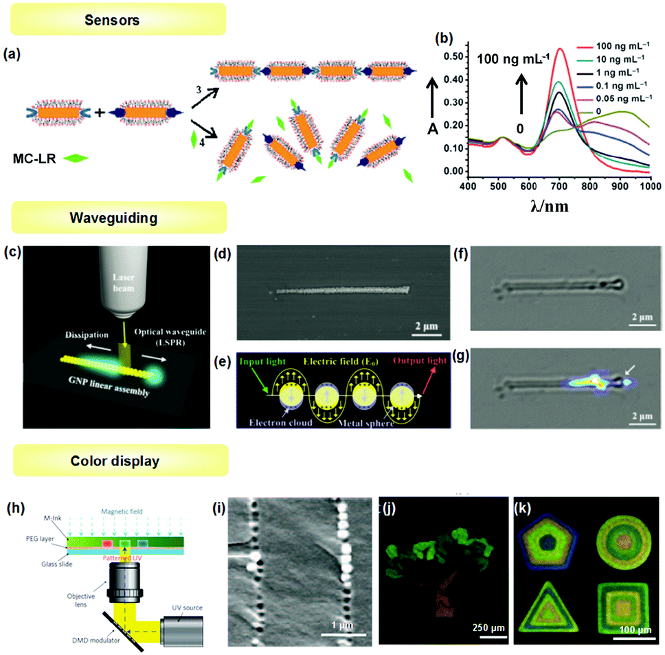 | ||
| Fig. 14 Applications of NPs’ 1D assemblies in photonics. (a and b) For sensing toxic molecules. In the presence of microcystin-LR (MC-LR) molecules, the GNR assembly would be dissociated, and the longitudinal plasmonic absorption peak shifted to the short wavelength. (c) For waveguiding. Schematic illustration of plasmonic waveguiding along the as-prepared GNP linear assembly. (d) SEM image and (f) bright-field optical micrograph of one GNP linear assembly. (e) Schematic illustration of the mechanism for LSPR propagation. (g) Waveguiding on both sides of the GNP 1D assembly. (h–k) For color display. (h) Schematic illustration of the 1D structure preparation. (i) SEM of assembled Fe3O4 NPs in resin. (j and k) Colored pattern due to 1D NP structure with different particle separations. (a and b) Are reproduced from ref. 6 with permission from Wiley-VCH Verlag GmbH & Co., copyright 2010; (c–g) are reproduced from ref. 5 with permission from Wiley-VCH Verlag GmbH & Co., copyright 2013; (h–k) are reproduced from ref. 36 with permission from the Nature Publishing Group, copyright 2009. | ||
Recent interest in 1D structure of metallic NPs (e.g., Au, Ag) focuses on its ability to transfer surface plasmon polaritons (SPPs) along the close-packed linear structure. In other words, with the facilitation of the near-field coupling between closely neighboring NPs, the 1D ordered NP structure can act as a waveguide to directionally transfer photons. Cheng et al.5 demonstrated the plasmonic waveguiding property of 1D assembled structures composed of monodispersed GNPs. The GNP 1D assemblies were prepared using the LBIA strategy as mentioned above. A strictly aligned GNP chain can be found in both SEM image (Fig. 14d) and bright-field optical image (Fig. 14e). Then, the waveguiding ability of the obtained NP 1D structure was investigated by focusing a 514 nm laser beam onto the GNP chain (Fig. 14c). After the laser beam was input to the GNP linear structure, photons were coupled with plasmonic resonances of linearly arranged GNPs, resulting in directional propagation of light (Fig. 14f). A bright spot on the right side and decreased light intensity along the left side of the GNP chain could be observed (Fig. 14g). Reducing the width of NP chains can decrease the transport loss while waveguiding. Song et al.44 tried to reduce the width of SNP chains down to around 100 nm, and obtained a slightly increased propagation distance of up to 3.2 μm. Thus, exploiting effective ways to reduce the transport loss of waveguiding along the NP 1D assembly is still a challenge.
1D arrays of magnetic NPs can be used in application of color displays due to their tunable 1D periodic structure and light reflectivity upon an external magnetic field. Yin et al. have developed a series of work on magnetically tunable photonic structures by assembling uniform superparamagnetic colloidal particles into 1D chain-like arrays.13 Herein, one example reported by Kwon et al. is illustrated to demonstrate the colour display application of NP 1D structures (Fig. 14h).36 The superparamagnetic colloidal nanocrystal clusters (CNCs) were first dispersed in a mixture of ethanol and photocurable resin. In the presence of an applied magnetic field, CNCs were assembled to form 1D chains, which were subsequently fixed by solidifying the resin through patterned ultraviolet exposure. The formed 1D chain structure was confirmed by SEM (Fig. 14i). The interparticle space of 1D chains could be tuned by exerting a magnetic field with different strengths, resulting in desired colours. By repetitive tuning and fixing the structure colour, programmed micropatterns with different colours were successfully attained (Fig. 14j and k).
3.3 Magnetics
1D arrays of magnetic NPs exhibit anisotropic and collective magnetic properties due to the strong anisotropic dipolar interaction, such as higher blocking temperature, increasing coercivity, and enhanced magnetothermal properties. For example, it was reported that the reduced remanent magnetization of the cobalt NP chains with a particle diameter of ca. 8 nm increased from 0.52 T to 0.60 T, compared to disordered NP aggregates.49 The increased magnetization was attributed to the strong anisotropic orientation of their magnetic moments along the 1D chain induced by the applied magnetic field. However, when the applied magnetic field was perpendicular to the alignment direction, the remanent magnetization was significantly decreased. Due to the unique magnetic characteristics, increasing interest has been generated in fabricating 1D assembled structures of magnetic NPs for a wide range of applications, including spintronics, biomedicine, water treatment, and sensors.Superparamagnetic NPs have been used as contrast-enhancement agents for magnetic resonance imaging (MRI). They can reduce the relaxation times of water and alter the nucleic magnetic resonance signal intensity. In one work reported by Gun’ko et al., 1D assemblies of magnetic Fe NPs (7–11 nm in diameter) were used as contrast agents for MRI in live rats. They found that the 1D structure could improve the contrast and the superior sinus sagittalis vein could be clearly seen for a Fast Low Angle Shot (FLASH) scan.7
Magnetic NPs (from superparamagnetic to stable ferromagnetic particles) subjected to an alternating magnetic field can serve as powerful heat sources for hyperthermic cancer treatment, arising from a magnetization reversal process of the particles. 1D structures of magnetic NPs exhibit superior heating performance over the randomly distributed system due to the coupling interaction between NPs. Specifically, Alphandery et al. reported high heating efficiency and antitumoral activity of the extracted chains of magnetosomes (γ-Fe2O3, ∼50 nm diameter) from magnetotactic bacteria, which were better than those of other materials, including inactive magnetotactic bacteria, individual magnetosomes, and chemically synthesized superparamagnetic iron oxide NPs.8 With administration of ∼1 mg of extracted chains of magnetosomes, and an alternating magnetic field (183 kHz and 40 mT for 20 min), a tumor xenografted under the skin of a mouse disappeared completely, while the other control materials exhibited lower efficiency for anticancer treatment.
Previous studies indicate that the 1D magnetosome chain found in magnetotactic bacteria possesses a permanent magnetic dipole, and acts as a critical orientation system. An artificial NP 1D structure was also found to present anisotropic magnetization characteristic, showing potential as a magnetic detector. Recently, Jiang, Mai and Yang et al.45 proposed an artificial magnetic-perception system, which was constructed by the alignment of superparamagnetic Fe3O4 NPs by using the LBIA strategy (Fig. 15a and b). Investigation indicated that all Fe3O4 NP 1D assembly with different widths displayed superparamagnetic nature and anisotropic magnetization due to their high-aspect-ratio structures. As shown in Fig. 15c and d, the magnetization intensity achieves a maximum value (Mmax) when the direction of B is parallel to the axis of Fe3O4 NP 1D assembly, whereas that has a minimum value (Mmin) when the direction of B is orthogonal with the axis of NP 1D assembly. The magnetic-perception ability of the artificial system can be explained by the coalescence of superparamagnetism and 1D architecture: the nonpermanent magnetic moment in superparamagnetic crystals can track the axis of the ambient magnetic field rapidly. Meanwhile, the high-aspect-ratio 1D architecture yielded anisotropic integrated magnetization intensity when the included angle (θ) between the axis of 1D assemblies and the direction of magnetic field was altered.
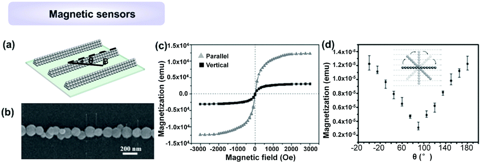 | ||
| Fig. 15 Applications of 1D assemblies of magnetic NPs for sensing magnetic field. (a) Schematic illustration of Fe3O4 NP 1D assemblies. The magnetic-perception ability was measured by changing the direction of magnetic field, θ. (b) SEM image of one Fe3O4 NP chain with width of ∼0.16 μm. (c) Magnetic properties of Fe3O4 NP chains with a width of ∼0.16 μm. (d) The curve illustrates the dependence of magnetization of Fe3O4 NP chains on θ. (a–d) are reproduced from ref. 45 with permission from Wiley-VCH Verlag GmbH & Co., copyright 2016. | ||
4. Conclusions and outlook
1D Self-assembly of NPs provides convenient yet powerful bottom-up ways for the creation of functional 1D nanostructures that can be deployed in the realization of multiple applications. This Tutorial Review discusses diverse strategies to organize NPs into 1D structures, and presents their typical and interesting applications in electronics, optics, and magnetics. Each approach has both advantages and challenges, which need to be properly selected to work in a certain situation for achieving NPs’ 1D assembly.Although 1D assemblies of NPs are ubiquitous in nature, research into their precisely controlled assembly and practical applications is still in its early stages. It's still often difficult to attain 1D assembly of NPs with a high degree of order on a large scale, which is essential for practical device applications of the 1D structure. For strategies based on inter-particle interactions, 1D assembled structures are usually obtained with a limited length ranging from several nanometers to tens of micrometers. The assembly of NPs achieved by external-force (e.g., electric field) can reach up to centimeters in length.15 Space-confined methods (e.g., PDMS-based template methods and LBIA) show great potential in applications of electronics due to their capabilities of creating 1D structures with tunable length and pre-designed pattern. The size and orientation of assembled 1D structures are strongly dependent on their applications. For example, the optical change of 1D structures of GNPs due to the plasmon coupling between NPs is related to the length of assembled structures but not with their orientations. Regarding this aspect, a recently published review paper50 is suggested for further reading. In terms of practical applications, on one hand, different strategies are possibly combined to improve the NP assembly quality. On the other hand, it's also anticipated that new and efficient strategies will be developed to realize precise 1D assembly of NPs with controllable alignment and positioning, which can be readily scalable and compatible with existing nanofabrication technologies. In the future, continuous efforts will be devoted to the applied research to improve the performance of the assembled structures.
Conflicts of interest
There are no conflicts to declare.Acknowledgements
This work was supported by the National 1000 Young Talents Program of China and initiatory financial support from HUST.Notes and references
- M. A. Boles, M. Engel and D. V. Talapin, Chem. Rev., 2016, 116, 11220–11289 CrossRef CAS PubMed.
- S. J. Barrow, A. M. Funston, X. Z. Wei and P. Mulvaney, Nano Today, 2013, 8, 138–167 CrossRef CAS.
- Z. Tang and N. A. Kotov, Adv. Mater., 2005, 17, 951–962 CrossRef CAS.
- E. Braun, Y. Eichen, U. Sivan and G. Ben-Yoseph, Nature, 1998, 391, 775–778 CrossRef CAS PubMed.
- B. Su, Y. Wu, Y. Tang, Y. Chen, W. Cheng and L. Jiang, Adv. Mater., 2013, 25, 3968–3972 CrossRef CAS PubMed.
- L. Wang, Y. Zhu, L. Xu, W. Chen, H. Kuang, L. Liu, A. Agarwal, C. Xu and N. A. Kotov, Angew. Chem., Int. Ed., 2010, 49, 5472–5475 CrossRef CAS PubMed.
- S. A. Corr, S. J. Byrne, R. Tekoriute, C. J. Meledandri, D. F. Brougham, M. Lynch, C. Kerskens, L. O'Dwyer and Y. K. Gun’ko, J. Am. Chem. Soc., 2008, 130, 4214–4215 CrossRef CAS PubMed.
- E. Alphandéry, S. Faure, O. Seksek, F. Guyot and I. Chebbi, ACS Nano, 2011, 5, 6279–6296 CrossRef PubMed.
- S. Lin, M. Li, E. Dujardin, C. Girard and S. Mann, Adv. Mater., 2005, 17, 2553–2559 CrossRef CAS.
- K. Liu, A. Lukach, K. Sugikawa, S. Chung, J. Vickery, H. Therien-Aubin, B. Yang, M. Rubinstein and E. Kumacheva, Angew. Chem., Int. Ed., 2014, 126, 2648–2653 CrossRef PubMed.
- S. Si, A. Kotal and T. K. Mandal, J. Phys. Chem. C, 2007, 111, 1248–1255 CrossRef CAS.
- Z. Nie, D. Fava, E. Kumacheva, S. Zou, G. C. Walker and M. Rubinstein, Nat. Mater., 2007, 6, 609–614 CrossRef CAS PubMed.
- Y. Hu, L. He and Y. Yin, Angew. Chem., Int. Ed., 2011, 50, 3747–3750 CrossRef CAS PubMed.
- R. Scirocco, J. Vermant and J. Mewis, J. Non-Newton. Fluid., 2004, 117, 183–192 CrossRef CAS.
- Z. Rozynek, M. Han, F. Dutka, P. Garstecki, A. Józefczak and E. Luijten, Nat. Commun., 2017, 8, 15255 CrossRef CAS PubMed.
- H. Kim, J. Kim, H. Yang, J. Suh, T. Kim, B. Han, S. Kim, D. S. Kim, P. V. Pikhitsa and M. Choi, Nat. Nanotechnol., 2006, 1, 117–121 CrossRef CAS PubMed.
- M. Vilfan, A. Potočnik, B. Kavčič, N. Osterman, I. Poberaj, A. Vilfan and D. Babič, Proc. Natl. Acad. Sci. U. S. A., 2010, 107, 1844–1847 CrossRef CAS PubMed.
- G. Hornyak, M. Kröll, R. Pugin, T. Sawitowski, G. Schmid, J.-O. Bovin, G. Karsson, H. Hofmeister and S. Hopfe, Chem. – Eur. J., 1997, 3, 1951–1956 CrossRef CAS.
- T. Teranishi, A. Sugawara, T. Shimizu and M. Miyake, J. Am. Chem. Soc., 2002, 124, 4210–4211 CrossRef CAS PubMed.
- D. Wang, Z.-C. Li and L. Chen, J. Am. Chem. Soc., 2006, 128, 15078–15079 CrossRef CAS PubMed.
- T. Kraus, L. Malaquin, H. Schmid, W. Riess, N. D. Spencer and H. Wolf, Nat. Nanotechnol., 2007, 2, 570–576 CrossRef CAS PubMed.
- Z. Deng, Y. Tian, S.-H. Lee, A. E. Ribbe and C. Mao, Angew. Chem., Int. Ed., 2005, 44, 3582–3585 CrossRef CAS PubMed.
- W. Li, S. Liu, R. Deng and J. Zhu, Angew. Chem., Int. Ed., 2011, 50, 5865–5868 CrossRef CAS PubMed.
- C.-L. Chen and N. L. Rosi, J. Am. Chem. Soc., 2010, 132, 6902–6903 CrossRef CAS PubMed.
- M. Ardini, F. Giansanti, L. Di Leandro, G. Pitari, A. Cimini, L. Ottaviano, M. Donarelli, S. Santucci, F. Angelucci and R. Ippoliti, Nanoscale, 2014, 6, 8052–8061 RSC.
- W. Han, M. Byun, B. Li, X. Pang and Z. Lin, Angew. Chem., Int. Ed., 2012, 51, 12588–12592 CrossRef CAS PubMed.
- J. X. Huang, F. Kim, A. R. Tao, S. Connor and P. D. Yang, Nat. Mater., 2005, 4, 896–900 CrossRef CAS PubMed.
- Z. Y. Tang, B. Ozturk, Y. Wang and N. A. Kotov, J. Phys. Chem. B, 2004, 108, 6927–6931 CrossRef CAS.
- J. H. Liao, Y. Zhang, W. Yu, L. N. Xu, C. W. Ge, J. H. Liu and N. Gu, Colloids Surf., A, 2003, 223, 177–183 CrossRef CAS.
- Z. Zhang, Z. Tang, N. A. Kotov and S. C. Glotzer, Nano Lett., 2007, 7, 1670–1675 CrossRef CAS PubMed.
- L. Zhu, D. Xue and Z. Wang, Langmuir, 2008, 24, 11385–11389 CrossRef CAS PubMed.
- D. Tan, S. Tu, Y. Yang, S. Patskovsky, D. Rioux and M. Meunier, J. Phys. Chem. C, 2016, 120, 21790–21796 CrossRef CAS.
- Y. Sun, B. Mayers, T. Herricks and Y. Xia, Nano Lett., 2003, 3, 955–960 CrossRef CAS.
- K. K. Caswell, J. N. Wilson, U. H. F. Bunz and C. J. Murphy, J. Am. Chem. Soc., 2003, 125, 13914–13915 CrossRef CAS PubMed.
- N. Sharma, A. Top, K. L. Kiick and D. J. Pochan, Angew. Chem., Int. Ed., 2009, 48, 7078–7082 CrossRef CAS PubMed.
- H. Kim, J. Ge, J. Kim, S.-E. Choi, H. Lee, H. Lee, W. Park, Y. Yin and S. Kwon, Nat. Photonics, 2009, 3, 534–540 CrossRef CAS.
- J. Bai, S. Huang, L. Wang, Y. Chen and Y. Huang, J. Mater. Chem., 2009, 19, 921–923 RSC.
- M. Volkmann, M. Meyns, R. Lesyuk, H. Lehmann and C. Klinke, Chem. Mater., 2017, 29, 726–734 CrossRef CAS.
- R. J. Tseng, C. Tsai, L. Ma, J. Ouyang, C. S. Ozkan and Y. Yang, Nat. Nanotechnol., 2006, 1, 72–77 CrossRef CAS PubMed.
- K. Sugikawa, K. Kaneko, K. Sada and S. Shinkai, Langmuir, 2010, 26, 19100–19105 CrossRef CAS PubMed.
- Y. Kondo, H. Fukuoka, S. Nakano, K. Hayashi, T. Tsukagoshi, M. Matsumoto and N. Yoshino, Langmuir, 2007, 23, 5857–5860 CrossRef CAS PubMed.
- E. Miele, S. Raj, Z. Baraissov, P. Kral and U. Mirsaidov, Adv. Mater., 2017, 29, 1702682 CrossRef PubMed.
- B. Su, S. Wang, J. Ma, Y. Wu, X. Chen, Y. Song and L. Jiang, Adv. Mater., 2012, 24, 559–564 CrossRef CAS PubMed.
- B. Su, C. Zhang, S. Chen, X. Zhang, L. Chen, Y. Wu, Y. Nie, X. Kan, Y. Song and L. Jiang, Adv. Mater., 2014, 26, 2501–2507 CrossRef CAS PubMed.
- X. Jiang, J. Feng, L. Huang, Y. Wu, B. Su, W. Yang, L. Mai and L. Jiang, Adv. Mater., 2016, 28, 6952–6958 CrossRef CAS PubMed.
- X. Jiang, Y. Wu, B. Su, R. Xie, W. Yang and L. Jiang, Small, 2014, 10, 258–264 CrossRef CAS PubMed.
- Y. Tang, B. Su, M. Liu, Y. Feng, X. Jiang, L. Jiang and A. Yu, Small, 2017, 13, 1601087 CrossRef PubMed.
- T. Shimada, K. Imura, H. Okamoto and M. Kitajima, Phys. Chem. Chem. Phys., 2013, 15, 4265–4269 RSC.
- C. Petit, V. Russier and M. P. Pileni, J. Phys. Chem. B, 2003, 107, 10333–10336 CrossRef CAS.
- M. Niederberger, Adv. Funct. Mater., 2017, 27, 1703647 CrossRef.
| This journal is © The Royal Society of Chemistry 2019 |