
Conductive diamond: synthesis, properties, and electrochemical applications
Nianjun
Yang
 *a,
Siyu
Yu
a,
Julie V.
Macpherson
*b,
Yasuaki
Einaga
c,
Hongying
Zhao
d,
Guohua
Zhao
*d,
Greg M.
Swain
e and
Xin
Jiang
*a
*a,
Siyu
Yu
a,
Julie V.
Macpherson
*b,
Yasuaki
Einaga
c,
Hongying
Zhao
d,
Guohua
Zhao
*d,
Greg M.
Swain
e and
Xin
Jiang
*a
aInstitute of Materials Engineering, University of Siegen, Siegen 57076, Germany. E-mail: nianjun.yang@uni-siegen.de; xin.jiang@uni-siegen.de
bDepartment of Chemistry, University of Warwick, Coventry, CV4 7AL, UK. E-mail: j.macpherson@warwick.ac.uk
cDepartment of Chemistry, Keio University, Yokohama 223-8522, Japan
dSchool of Chemical Science and Engineering, Tongji University, Shanghai 200092, China. E-mail: g.zhao@tongji.edu.cn
eDepartment of Chemistry, Michigan State University, Michigan 48824, USA
First published on 16th November 2018
Abstract
Conductive diamond possesses unique features as compared to other solid electrodes, such as a wide electrochemical potential window, a low and stable background current, relatively rapid rates of electron-transfer for soluble redox systems without conventional pretreatment, long-term responses, stability, biocompatibility, and a rich surface chemistry. Conductive diamond microcrystalline and nanocrystalline films, structures and particles have been prepared using a variety of approaches. Given these highly desirable attributes, conductive diamond has found extensive use as an enabling electrode across a variety of fields encompassing chemical and biochemical sensing, environmental degradation, electrosynthesis, electrocatalysis, and energy storage and conversion. This review provides an overview of the fundamental properties and highlights recent progress and achievements in the growth of boron-doped (metal-like) and nitrogen and phosphorus-doped (semi-conducting) diamond and hydrogen-terminated undoped diamond electrodes. Applications in electroanalysis, environmental degradation, electrosynthesis electrocatalysis, and electrochemical energy storage are also discussed. Diamond electrochemical devices utilizing micro-scale, ultramicro-scale, and nano-scale electrodes as well as their counterpart arrays are viewed. The challenges and future research directions of conductive diamond are discussed and outlined. This review will be important and informative for chemists, biochemists, physicists, materials scientists, and engineers engaged in the use of these novel forms of carbon.
 Nianjun Yang | Dr Nianjun Yang is a senior scientist and group leader at the Institute of Materials Engineering, University of Siegen, Germany. He works on the growth and electrochemical applications of advanced carbon materials. He has published more than 120 journal papers, edited 4 books, contributed 9 book chapters, organized 7 European Materials Research Society symposiums, and acted as the guest-editor of several journals. He is currently editing 1 book series, working as the editor board member of the journals of Scientific Reports and Diamond and Related Materials as well as the program committee member of several diamond related international conferences. |
 Julie V. Macpherson | Dr Julie V. Macpherson is a Professor in the Department of Chemistry, University of Warwick and is also a Royal Society Industry Fellow. Her current work is on the development of conductive diamond platforms for electrochemical applications. She has published over 170 papers and filed 15 patents. She has won the RSC Marlow Medal and the McBain medal. In 2016 she was named as one of the Top 50 Women in Analytical Science. She is currently significantly involved with the CDT Training Centre for PhD scientists in Diamond Science and Technology at Warwick University. |
 Yasuaki Einaga | Dr Yasuaki Einaga is a Professor in the Department of Chemistry at Keio University, Japan. He was also a research director of JST-CREST (2011–2014) and now he is a research director of JST-ACCEL (from 2014). His research interests include functional materials science, photochemistry, electrochemistry, and diamond electrodes. He has published more than 200 papers in peer-reviewed journals, edited 1 book, contributed 4 book chapters, and delivered more than 40 invited talks at international conferences. He has organized international symposiums on diamond electrochemistry in Japan (2004, 2005, 2007, 2014). |
 Guohua Zhao | Dr Guohua Zhao is a professor at School of Chemical Science and Engineering, Tongji University, China, where he obtained his PhD degree in environment in 1999. After one year as a visiting fellow at University of Stuttgart, he joined the School of Chemical Science and Engineering, Tongji University. His current research interests include photoelectric catalysis and environmental energy chemistry using diamond and diamond/metal oxide composites, committed to cross field research work of environment and energy, such as CO2 reduction, hydrogen production, photoelectrocatalytic oxidation and analysis of pollutants. Up to now, he has published 1 academic book and 150 research papers in peer-reviewed journals. |
 Greg M. Swain | Dr Greg M. Swain is a Professor in the Department of Chemistry, Michigan State University. His group's current research is at the crossroads of carbon materials science and physical and analytical electrochemistry. The current projects include diamond and diamond-like carbon electrodes for electroanalysis, optically transparent diamond electrodes for spectroelectrochemistry, nanocarbon powders as advanced materials for separations, and diamond microelectrodes for neuroanalytical chemistry and chemical and biochemical sensors. He previously served as Editor and Editor-in-Chief of Diamond and Related Materials (Elsevier) (2011–2015) and he currently serves on the advisory board of Advanced Engineering Materials (Wiley). |
 Xin Jiang | Dr Xin Jiang has been a professor and the chair holder of Surface and Materials Technology at University of Siegen (Siegen, Germany) since 2003. He received the award “State Specially Recruited Expert” of China in 2013. He was a Changjiang-Visiting Chair Professor at Dalian University and Science and Technology, China. His current research fields cover the growth and applications of diamond thin films, nanomaterials as well as materials characterization. He has published over 320 peer reviewed journal papers, and contributed 8 books and book chapters. He has delivered numerous invited talks/lectures at international conferences. |
1. Introduction
Carbon is an extraordinary element because of its ability to covalently bond with different orbital hybridization. This leads to a rich variety of molecular structures that constitute the field of organic chemistry.1 For millennia, there were only two known substances of pure carbon: graphite and diamond. The carbon atoms in graphite are sp2 hybridized, with an interplanar C–C bond length of 1.42 Å and an interplanar spacing of 3.354 Å. A diamond crystal has a face centred cubic structure. Its carbon atoms are sp3 hybridized and tetrahedrally arranged with a C–C bond length of 1.54 Å.2 In the mid-1980s a new carbon allotrope, C60 (or buckminsterfullerene), was discovered by Curl, Kroto, and Smalley, who were awarded the 1996 Nobel Prize in Chemistry. C60 possesses a soccer-ball shape.3 In the early 1990s, carbon nanotubes (CNTs) were discovered.4 They are direct descendants of fullerenes and contain capped tubular structures composed of 5- and 6-membered rings. The large aspect ratio (length to diameter) and crystalline order along the tubes give CNTs unique properties, e.g. high conductivity, thermal stability, flexibility, reactivity, etc.5 In the early 2000s, graphene, a single sheet of carbon atoms arranged in a hexagonal lattice with a bond distance of 1.42 Å, was reported by Geim and Novoselov,6 who were awarded the 2010 Nobel Prize in Physics. Owing to the semi-metallic band structure, this 2D material features interesting electrical properties and presents many useful applications.7The physical, chemical and electronic properties of these carbon allotropes differ from each other since they are determined by their carbon–carbon covalent bonding and the organization of the carbon atoms in their characteristic micro-structures.2,8 For example, the exceptional properties of diamond arise because (i) carbon atoms are relatively small and light, with short range bonds in the lattice, and (ii) these bonds are covalent, sp3 hybridized in a tetrahedral arrangement and strong. This results in very high material hardness and thermal conductivity. Diamond also possesses extremely low electrical conductivity unless doped e.g. with boron, to significantly increase conductivity, a key property of the material for any electrochemical application.
The first introduction of diamond into electrochemistry was reported in 1983 by Iwaki et al.,9 who used ion-implanted diamond as an electrode. In 1987 Pleskov et al.10 explored the photoelectrochemistry of a thin polycrystalline diamond film grown on a tungsten substrate. It was stated10 that this semi-conductor consisted of more than 99% carbon in the diamond crystalline form containing small amounts of chemical (H, O, N) and phase (non-diamond forms of carbon) impurities. Later Fujishima et al. investigated the photoelectrochemical response of semi-conducting boron-doped diamond (BDD) films11 and further applied them as photoelectrodes.12 The early 1990s saw the emergence of electrically conducting diamond as a new carbon electrode material for different electrochemical applications.13–19 In 1993 Tenne et al.13 and Swain et al.14 employed BDD for electroanalytical applications. In the same year Loo et al. showed the advantages of BDD as a stable anode for electrochemical wastewater treatment.15 Miller et al.16 and Carey et al.17 conducted anodic oxidation of organic wastes using dimensionally stable BDD anodes. In 1996, the wide electrochemical potential windows of high quality BDD were revealed by Angus et al.20 Work that followed increased in intensity with researchers widely recognizing BDD as an electrode that features extremely interesting electrochemical properties beyond those offered by conventional electrode materials. Over the past four decades, conductive diamond, including BDD, nitrogen-doped diamond (NDD), phosphorus-doped diamond (PDD), and hydrogen-terminated undoped diamond, has been utilized in various fields of electrochemistry for different applications.2,21–30 Among them, BDD has been the most extensively employed due to the fact that it can be highly doped. For non-boron-doped diamond films (e.g., NDD, PDD) and undoped hydrogen-terminated diamond, it is not possible to achieve the high electrical conductivity that can be obtained through boron doping.
This review begins with a general introduction of diamond growth (Section 2), focusing on the use of chemical vapour deposition (CVD) techniques to synthesize doped diamond films. The formation of conductive diamond nanostructures e.g. by means of top-down, bottom-up, and template-free approaches and the production of conductive diamond particles are briefly overviewed. Starting with the surface properties of conductive diamond (e.g., surface terminations, surface reactivity), Section 3 deals mainly with the electrochemical properties of conductive diamond (e.g., background currents, potential window, redox response) as well as the effect of dopants, non-diamond carbon (NDC) presence, crystal structure, surface terminations, etc. on these properties. Section 4 details the applications of conductive diamond in the fields of electroanalysis, environmental degradation, electrosynthesis, electrocatalysis, and electrochemical energy storage. Before closing this review, the fabrication and characterization of diamond electrochemical devices (e.g., small-dimensional diamond electrodes and their arrays, scanning probes, and energy devices) is shown in Section 5. To conclude, the technological challenges and future research directions of conductive diamond are discussed and outlined in two areas: the growth of conductive diamond and potential electrochemical applications.
2. Synthesis
2.1 CVD synthesis of diamond films
Artificial diamond synthesis by the high-pressure high-temperature (HPHT) method was first reported in 1955 at General Electric31 where graphite was converted to diamond. Eversole et al. documented the first report on diamond growth at low pressure.32 In the early 1970s, a major breakthrough was achieved in the CVD diamond growth process when atomic hydrogen was used during growth. The process also permits the nucleation of new diamond crystallites on non-diamond substrates. This work was extended by e.g. Angus et al. at Case Western University33–36 and by Deryagin and co-workers at the Physical Chemistry Institute in Moscow.37–39Research into CVD diamond growth started in earnest in the early 1980s, pioneered independently by J. Angus in the USA and by V. Varnin in the USSR. Pioneering work by a Japanese group at the National Institute for Research in Materials at Tsukuba under the leadership of Setaka described the use of different CVD techniques such as hot-filament CVD (HFCVD),40,41 microwave plasma CVD (MWCVD),42 and radio-frequency plasma CVD (RFCVD)43,44 for diamond growth.32 Such developments initiated the growth of numerous global diamond research programmes ranging from: technique development, e.g. diamond coating processes, diamond coating on various substrates, etc.; a mechanistic understanding of CVD diamond nucleation and growth; doping of CVD diamond; characterization and property investigation of CVD diamond, e.g., optical, electronic, thermal, mechanical, etc.; and applications in the physical, engineering, chemical, biomedical, and related fields.32,45
The growth of diamond from the vapour phase on a non-diamond substrate, at a practical rate, requires a hydrocarbon gas (usually methane) mixed in low concentration with hydrogen. Hydrogen is critical for several aspects of growth, in particular, the abstraction of H from both gas phase methane to produce a growth precursor (radical), CH3˙, and from H-terminated surface sites to produce active radical sites for carbon radical addition. Hydrogen also etches NDC much faster than it does diamond, allowing NDC co-deposits to be removed and a much higher growth rate of diamond to be realized. The gases need to be activated and this is typically done by thermal- or plasma-assisted CVD processes. Although CVD techniques are different in the process details, they do own many common features: (i) diamond growth in the presence of atomic hydrogen, (ii) dissociation of carbon-containing source gases, and (iii) diamond growth at moderate substrate temperatures, e.g. typically between 500 and 1200 °C.46–48 The majority of carbon radicals, necessary for the growth of diamond, originate from the dissociation of the carbon-containing gas precursor by means of hot-filament, RF-plasma or microwave plasma, etc. The growth substrate can be either bulk diamond (either natural or synthetic) or a non-diamond substrate, leading to homoepitaxial (single crystalline) or hetero (polycrystalline) growth of diamond films, respectively. Polycrystalline diamond films consist of crystallites with different orientations and associated grain boundaries; in contrast single crystal diamond has no grain boundaries. Since diamond does not grow spontaneously on non-diamond materials, an extra “seeding” step is usually required for deposition on a foreign substrate. For example, the non-diamond substrate can be decorated with diamond nanoparticles (NPs) that serve as initial nucleation sites for growth. Such diamond seed coated substrates then grow three-dimensionally until the grains coalesce, forming a continuous polycrystalline diamond film. The average grain size of polycrystalline diamond films deposited from hydrogen-rich gas mixtures increases as a function of film thickness, which in turn is controlled by growth time.49
Polycrystalline diamond can also be deposited from argon-rich gas mixtures as demonstrated in the pioneering work by Gruen and co-workers at Argonne National Laboratory.50–57 These films contain varied ratios of diamond (sp3-carbon) to NDC (sp2-carbon). This is in contrast with hydrogen rich gas mixtures, where the average grain size of polycrystalline diamond films deposited from hydrogen-rich gas mixtures increases as a function of film thickness or the growth time.49 The high rate of re-nucleation achieved during argon-rich growth prevents the crystallites from getting larger with growth time. Such films are referred to as ultrananocrystalline diamond (UNCD).51,58–60 Polycrystalline films are generally classified based on their crystallite or grain size as either microcrystalline diamond (MCD) or nanocrystalline diamond (NCD) and are typically grown under hydrogen-rich atmospheres.55–57 UNCD films thus have a much higher surface to volume ratio than their microcrystalline counterparts and more extensive π-bonding and sp2 hybridization given the higher NDC content of this material, typically residing in grain boundaries. These films also possess intrinsic electrical conductivity due to the π-states in the bandgap47,48 and this is a reason why undoped UNCD films find use in some electrochemical applications. UNCD films deposited from Ar-rich source gas mixtures are not faceted but rather possess a nodular morphology with negligible crystal faceting. Theoretical results suggest that the nanocrystalline morphology results, at least in part, because of a high rate of re-nucleation due to the C2 dimer produced during CVD processes using Ar-rich source gas mixtures.50–57 These UNCD films are very different morphologically and microstructurally from NCD films as the UNCD films possess a smaller grain size and more grain boundaries.
2.2 Doping of CVD diamond films
Diamond with metal-like conductivity is generally required for most electrochemical applications. Controlled doping is accomplished by the addition of appropriate elements (e.g., boron, nitrogen, or phosphorus) during CVD growth. The substitutional insertion of these non-carbon elements imparts electrical conductivity to the diamond, the characteristics of which depend on the dopant and level of doping. At low doping levels, ≤1019 atoms cm−3, the diamond behaves electrically and electrochemically as a p- or n-type semiconductor, depending on the dopant type. It is the substitutionally inserted impurity atoms that contribute to the electrical properties. Dopant atoms can also be segregated in the grain boundaries but these are generally not electrically active. For this reason, actual doping levels measured are higher than the determined carrier concentrations. At high doping levels, ≥1020 atoms cm−3, the material behaves as a semi-metal and possesses high electrical conductivity.Phosphorus,61 sulphur and arsenic,62 and boron and nitrogen63 have all been reported as dopants for diamond. Among them, boron and then nitrogen are the most widely accepted, and are used to produce p- and n-type conductive materials, respectively, although it is only boron that can be added in high enough concentrations to achieve metal-like conductivity due to the small atomic radius of boron. Boron-doped MCD, NCD, and UNCD have all been used in electrochemistry.64 Electrochemical properties of boron-doped UNCD are similar to those of boron-doped MCD and NCD films.55–57 The source of boron is generally gas-phase diborane or trimethyl borane, diluted in hydrogen. Since boron is electron-deficient relative to carbon, the doping level of such a p-dopant can be in the range of 1018–1021 atoms cm−3, which corresponds to a boron-to-carbon ratio of about 10−5 to 10−3. When the doping level reaches values higher than 1020 cm−3, the conduction mechanism of these heavily doped films changes and the activation energy approaches zero.65 Therefore, these films are the most suitable as electrodes for electrochemical applications, and feature predominantly in this review.66
When diamond films containing very large concentrations of boron to carbon (>0.25%) are cooled to below −200 °C, they are shown to offer no resistance to the flow of electricity, i.e. they are superconducting.67 Such superconductivity was for the first time discovered in metal-like polycrystalline BDD synthesized at pressure (8–9 GPa) and temperature (2500–2800 K) by Ekimov et al.68,69 with a superconducting transition temperature (Tc) of 4 K. Kawarada et al. recorded the highest Tc (=7.4 K) using single crystal (111) BDD; Tc = 3.2 K for (100) BDD.70–75 Currently, the superconductivity of BDD is mostly of academic interest as the temperature at which it becomes superconducting is very low. However, there are some devices such as the Superconductive Quantum Interference Devices, used for the detection of very small magnetic fields, where this property of BDD could have real world applications in the future.76
Other doped diamond films have been synthesized. For example, NDD films were grown using a HFCVD process and their conductivity was recorded to be several mS cm−1, tens to hundreds of times higher than that for metal-like BDD.77 Nitrogen-doped UNCD films have been grown on silicon78,79 or titanium substrates using plasma-assisted CVD.80 Nitrogen diluted with a mixture of methane, argon78 or hydrogen,79,80 or with triethylamine dissolved in methanol81 is generally used as a nitrogen source. Recently, hot-cathode-direct-current plasma CVD (HCDCPCVD) has been used to grow NDD films, achieving a maximum electrical conductivity of 5 S cm−1.82 The PDD films have been grown on IIa type single crystalline diamond83 and p-type Si substrates.84 The measured phosphorus concentrations were 7.4 × 10¹⁸ and 1.8 × 1018 cm−3, respectively. In both cases, plasma-assisted CVD was used. The sources of the phosphorus dopant, carbon, and carrier gas were phosphine, methane, and hydrogen, respectively. Note that, doping levels of nitrogen, phosphorus, and sulphur in diamond films are not high (generally <1019 atoms cm−3). Thus, the electronic properties of such diamond films are semiconducting at best. However, the measured electrical conductivity (and the resulting electrochemical behaviour) suggests higher doping, which is not possible, and indicates other factors such as NDC and hydrogen content (Sections 3 and 4) playing a role.
Any diamond substrate that emerges from the CVD growth chamber is hydrogen terminated due to the hydrogen rich growth atmosphere terminating the dangling bonds on the diamond surface with hydrogen. Due to this hydrogen termination, undoped, as grown CVD diamond shows p-type surface induced conductivity once it is immersed in electrolyte solutions (Section 3.1).85,86
2.3 Conductive-diamond nanostructures
Various conductive-diamond nanostructures (e.g., nano-pillars, nanowires, pores, foams, etc.) have been fabricated using top-down, bottom-up, and template-free approaches.23,87,88 In the top-down approach, BDD is selectively etched away with reactive ions through a hard mask. The applied etching gas (e.g., O2), etching masks (e.g., size, shape, etc.), and the etching conditions (e.g., temperature, gas atmosphere, pressure, power, time, etc.) determine the sizes, lengths, and densities of the as-fabricated nanostructures. Various mask materials (e.g., Al, Au, Ni, Mo, polymers, oxides, nitrides, diamond nanoparticles, etc.) have been used. In the bottom-up approach, diamond nanostructures are produced by the CVD overgrowth of the patterned templates with MCD, NCD or UNCD films. In this way, various diamond nanostructures (e.g., vertically aligned wires, diamond foams, porous membranes, etc.) have been formed. Silicon nanowires, CNTs, silicon oxide spheres and highly porous polypyrrole scaffolds have been employed as templates.23,87,88 A variety of template-free techniques have also been used, for example, selective and wet-chemical removal of cubic SiC from a diamond–SiC composite film to produce diamond networks.89 Porous BDD has been formed by (i) thermal etching of diamond via a two-step process: graphitization of the BDD film surface by heating in an argon atmosphere at 1000 °C followed by removal of the graphitic layer by oxidation in air at 425 °C90 and (ii) oxidative etching of BDD electrodes with steam or CO2.91–93Fig. 1A shows typical examples of BDD nanostructures including diamond networks,89 diamond paper,94 diamond honeycomb,95 porous diamond,96 and diamond nanowires.97 | ||
Fig. 1 (A) SEM images of diamond networks (a),89 diamond paper (b),94 porous diamond (c),96 and diamond nanowires (d).97 Reprinted with permission from ref. 89. Copyright 2017, American Chemical Society; from ref. 94. Copyright 2016, American Chemical Society; from ref. 96. Copyright 2017, Elsevier; from ref. 97. Copyright 2016, American Chemical Society. (B) SEM images of NDD nanoplate (a),98 vertically aligned NDD microwire arrays (b and c),99,100 and nanorods (d).101 Reprinted with permission from ref. 98. Copyright 2013, Royal Society Publisher; from ref. 99. Copyright 2015, Elsevier; from ref. 100. Copyright 2014, Elsevier; from ref. 101. Copyright 2017, Elsevier. (C) Schematic plot of the structure of NDD (a).102 Reprinted from ref. 102. Copyright 2005. Elsevier. TEM image of BDD nanoparticles (b). Reprinted with permission from ref. 109. Copyright 2014. American Chemical Society. SEM micrographs of (c, left) boron-doped UNCD deposited on GC powder 5 μm in diameter (15![[thin space (1/6-em)]](https://www.rsc.org/images/entities/char_2009.gif) 000×). Reprinted with permission from ref. 107. Copyright 2009. American Chemical Society. (d, right) Graphene nanopetals formed on GC powder (9500×). The boron-doped UNCD phase was formed using 1% methane and the nanopetal phase was formed using 3% methane in the source gas mixture. The white scale bars in both images are 1 μm in dimension. Reprinted with permission from ref. 107. Copyright 2009. American Chemical Society. 000×). Reprinted with permission from ref. 107. Copyright 2009. American Chemical Society. (d, right) Graphene nanopetals formed on GC powder (9500×). The boron-doped UNCD phase was formed using 1% methane and the nanopetal phase was formed using 3% methane in the source gas mixture. The white scale bars in both images are 1 μm in dimension. Reprinted with permission from ref. 107. Copyright 2009. American Chemical Society. | ||
Several conductive NDD nanostructures have also been synthesized. For example, NDD nanowires were grown on planar Si substrates using a MWCVD method in which methane (6%) and nitrogen (94%) were the sources of carbon and nitrogen dopant, respectively.98 NDD microwires and vertically aligned NDD arrays were produced by overgrowing on titanium alloy microneedles99 and Si wires.100 NDD nanorods were fabricated via direct reactive ion etching of nanocrystalline NDD films, grown using the MWCVD technique (Fig. 1B).101
2.4 Conductive diamond particles
Detonation processes using explosive molecules and graphite precursors have been widely applied to produce NPs or powders of diamond. The resulting diamond is called detonation nanodiamond (DND) and has a core–shell structure (Fig. 1C).102 The sp3 diamond core features a size of 4–5 nm, while the outer shell consists of a mixture of sp2 and sp3 carbon as well as oxygen-containing functional groups (e.g., carboxylic acids, esters, lactones, quinones). BDD particles can be produced via a core shell approach, which is overgrowth of a substrate powder, e.g. glassy carbon (GC) or insulating diamond powder, with an overlayer of BDD.103–107 For example, the resulting surface area of the conducting powders can be varied from a few to 100's m2 g−1 by simply reducing the diameter of the substrate powders. To date, diamond abrasive powder (nm to μm diameters)103–106 and GC powder107 have been over-coated with boron-doped UNCD. A range of carbon nanostructures can, in fact, be produced through adjustments in the source gas ratio (e.g., methane to argon or hydrogen) at constant power (e.g. 800 W) and system pressure (e.g., 120–140 torr). For example, various nanostructured carbons have been produced ranging from boron-doped UNCD-coated (using 1% ratio methane) and graphene nanopetal-coated (when using higher methane levels, 3–5%) GC powders. Fig. 1C shows SEM micrographs of boron-doped UNCD- and nanopetal-coated GC powders. The GC substrate powder is 5 μm in diameter. The boron-doped UNCD phase readily nucleates and grows directly on carbon substrates that are microstructurally disordered at the surface with a high fraction of exposed graphitic edge plane, such as GC.107 The edge plane sites serve as the initial nucleation sites for diamond growth.107 UNCD (cauliflower-shaped features) can be observed over-coating the powder surface. The 50–100 nm nodular features present are aggregates of diamond grains that are in the 5–10 nm range. The specific surface area of this coated material is 2–5 m2 g−1 and the electrical conductivity is 2–5 S cm−1. The graphene nanopetal phase can be seen on the surface of the GC powders. The nanopetals are graphitic carbon and they decorate the surface with lengths of several hundred nanometers and heights of several tens of nanometers.107BDD powders can also be produced by milling of BDD films. BDD films were synthesized under HPHT using B-doped graphite intercalation compositions as carbon sources.23,108 Recently, small-sized BDD particles (10–60 nm) were produced by multistep milling of nanocrystalline BDD films, followed by purification and surface oxidation.109
3. Properties
In comparison to other widely employed carbon electrode materials, conductive diamond features multiple unique physical and chemical properties.2,110,111 For example, it is chemically inert, does not swell in electrolyte solutions, and is biocompatible. Weak or no surface bio-fouling has been reported on conductive diamond surfaces. Moreover, it exhibits high chemical stability in harsh environments, at high current densities and potentials. It is ultrahard and thus can be textured with dimensions of typically a few nanometers112–114 to nanowires with lengths of a few micrometers.115 In Section 3.1, further details regarding surface termination, surface reactivity, and electrochemical properties of conductive diamond are provided. The experimental effects of dopants (in particular boron), NDC content, crystal structure, and post-treatment are also reviewed. The vast majority of the discussion will be focused on BDD, given its wide spread use as an electrode material.3.1 Surface termination
The diamond surface can be terminated in various ways originating from its rich carbon chemistry. Once the surface atoms of diamond are fully bonded with hydrogen, the surface is hydrogen-terminated (or hydrogenated). It features hydrophobic properties where water contact angles are as high as ∼90°. Such a hydrogen-terminated surface (–Cδ−–Hδ+) increases the energy levels of both valence band (EVB) and conduction band (ECB) of diamond at the surface. Since ECB sits above the vacuum level, a negative electron affinity develops. Once the hydrogen-terminated diamond is immersed in aqueous solutions, electron transfer (ET) between H3O+ and EVB becomes possible (even without doping). A positively charged accumulation layer is formed near the surface leading to a measurable surface conductivity on insulating diamond, as explained by the surface-transfer doping model.86 A hydrogen-terminated diamond surface can be achieved by different approaches such as hydrogen plasma treatment and cathodic electrochemical treatment (e.g., application of −35 V for 5 min in 2 M hydrochloric acid solution).116 Although a hydrogen-terminated BDD surface is generally stable in air or in solutions for several months, it does slowly oxidize over time in air or via exposure to solution.117,118When a hydrogen-terminated diamond surface is partially or fully oxidized, the surface becomes hydroxylated or oxygen-terminated (or oxygenated), respectively. The oxygen functional groups are a mixture of –OH, –C–O–C– and >C![[double bond, length as m-dash]](https://www.rsc.org/images/entities/char_e001.gif) O.116 An oxygen-terminated surface (Cδ+–Oδ−) has an opposite bond polarity compared to the hydrogen-terminated one (–Cδ−–Hδ+) that typically lowers the energy levels relative to the vacuum level. This results in a positive electron affinity. Oxygen-terminated diamond surfaces are hydrophilic with water contact angles from 0.6° to 65°, depending on the oxidation method, surface roughness, dopant level, etc.119 A variety of methods have been used to oxygen terminate diamond surfaces, such as wet-chemical treatment (e.g., boiling in acids or acid mixtures),120 dry-chemical oxidation (e.g., photochemical or ozonation oxidation,121 treatment in O2 at high temperatures122), mechanical treatment (e.g., alumina polishing),123 plasma treatment (e.g., O2),57,124 and electrochemical oxidation.116,124–127 On single crystalline diamond, specific crystal faces support specific oxygen functionalities. For an oxygen-terminated single crystal diamond, C–OH groups are the most abundant on the (111) face. The –C–O–C and >CO (and more highly oxidized) groups dominate on the (100) face.128
O.116 An oxygen-terminated surface (Cδ+–Oδ−) has an opposite bond polarity compared to the hydrogen-terminated one (–Cδ−–Hδ+) that typically lowers the energy levels relative to the vacuum level. This results in a positive electron affinity. Oxygen-terminated diamond surfaces are hydrophilic with water contact angles from 0.6° to 65°, depending on the oxidation method, surface roughness, dopant level, etc.119 A variety of methods have been used to oxygen terminate diamond surfaces, such as wet-chemical treatment (e.g., boiling in acids or acid mixtures),120 dry-chemical oxidation (e.g., photochemical or ozonation oxidation,121 treatment in O2 at high temperatures122), mechanical treatment (e.g., alumina polishing),123 plasma treatment (e.g., O2),57,124 and electrochemical oxidation.116,124–127 On single crystalline diamond, specific crystal faces support specific oxygen functionalities. For an oxygen-terminated single crystal diamond, C–OH groups are the most abundant on the (111) face. The –C–O–C and >CO (and more highly oxidized) groups dominate on the (100) face.128
The diamond surface can be also terminated with halogens (e.g., –F, –Cl, etc.)129–132 These halogenated diamond surfaces are hydrophobic: a controversial phenomenon known as polar hydrophobicity. Halogenation with fluorine and chlorine is possible by activating a halogen gas to form free radicals (under high temperature or ultra-high vacuum conditions). A milder approach is to employ ultraviolet (UV) photochemical activation in the presence of the halogen gas.133 The Cl-terminated surface is not very stable in air and readily converts to an oxygen-terminated surface. Furthermore, nitrogen (e.g., –N, –NH, –NH2) terminated diamond surfaces (in most cases so-called aminated surface) have been realized directly using a plasma in the presence of ammonia.134–136
X-ray photoelectron spectroscopy (XPS) and contact angle measurements are frequently employed to characterize the diamond surface chemistry.57 From the related binding energies for different carbon bonds (e.g., C–O–C, CO, C–F, C–Cl, C–N, etc.), XPS is especially useful for semi-quantitative characterization of hydroxylated, oxygenated, halogenated, and aminated diamond surfaces.57,127 However, XPS cannot deliver quantitative information on hydrogen-terminated diamond surfaces.116,137,138 Electrochemical techniques (e.g., voltammetry, impedance)116 and selective grafting of diazonium salts137,138 have also been employed as indirect ways to characterize the hydrogen-terminated diamond surface.
3.2 Surface reactivity
A variety of functionalization strategies have been used to chemically modify conductive MCD, NCD and UNCD surfaces. In general, the functionalization routes are of four types: chemical, photochemical, thermal, or electrochemical.139–143 These functionalized surfaces can be used directly in electrochemical measurements or be further functionalized with target moieties depending on the desired application.Photochemically, UV irradiation of hydrogen-terminated diamond covered with a liquid film of the appropriate alkene (one end vinyl terminated, the other end terminated appropriately for the application of interest, e.g. amine,144 carboxylate145) has been employed for grafting organic layers to the diamond surface via a C–C bond.146 Direct amination of the hydrogen-terminated surface is also possible using UV treatment in the presence of a long chain end group protected amine (UV only).147 Chemically, amino-silane groups can be produced by reacting oxygen terminated diamond with 3-aminopropyltriethoxysilane (APTES). Thermally activated formation of alkene-derived self-assembled monolayers has been also realized on oxygen-terminated diamond surfaces: hydrogen-terminated diamond sites remained unaffected during such a process. This approach is thus complementary to the UV-initiated reaction of alkenes with diamond, which only goes via the hydrogen-terminated surface.143 Electrochemically, reduction of diazonium salts on BDD electrodes is also useful.112,113,148,149 For example, primary amines and aromatic hydrocarbons (aryl diazonium salts) have been grafted to the diamond surface using this procedure. The diazonium modification can produce monolayer or multi-layer coverage, if continued radical addition is allowed to occur. The grafting efficiency has also been linked to the boron dopant density of the electrode.150 Diazonium modification is versatile and can be used to introduce a wide variety of functional groups (e.g., –COOH, X, NO2, etc.) onto the electrode surface.137,151
3.3 Electrochemical properties
BDD exhibits unique electrochemical properties and thus presents many advantages for use over classical metal electrodes and other sp2 carbon electrodes. These include low and stable background currents, a wide electrochemical potential window, weak molecular adsorption, microstructural stability, and relatively rapid ET kinetics for multiple soluble redox systems often without electrode pretreatment.NDD and BDD electrodes grown by HFCVD showed similar electrochemical potential windows.77,82 As the NDD was semi-conducting, it was thought that NDC impurities present in the electrode were responsible for the solvent window similarity. In situ Raman spectroelectrochemical measurements showed that subsequent progressive cycling between −2.5 and 2.5 V (vs. Ag/AgCl) electrochemically removed these electrocatalytic impurities, leading to an increase of the potential window.84 This study also highlighted the need to understand the material surface composition when interpreting the electrochemical response of the electrode.
The surface roughness differences of microcrystalline and nanocrystalline films do not generally affect diffusion-limited currents for redox analytes at conventional scan rates as the diffusion layer thickness is greater than the roughness dimensions.128 For example, the voltammetric behavior of Fe(CN)63−/4− and Ru(NH3)62+/3+ recorded on polycrystalline BDD appears similar to that on a GC or platinum electrode,160 exhibiting close to reversible characteristics (diffusion-limited). This is true for Fe(CN)63−/4− if the diamond electrode surface is clean and presents a specific oxygen functionality.60,161 Heterogeneous ET rate constants for a variety of aqueous redox probes are in the 10−3 to 10−1 cm s−1 range.60,128,161 These rate constants were determined from cyclic voltammetric ΔEp–scan rate trends and digital simulation, where ΔEp is the potential difference between the anodic and cathodic peaks.
When using techniques such as scanning electrochemical microscopy (SECM)154 or Fourier transformed alternating current voltammetry,162 which can more accurately determine high ET rate constants, it has been found that the outer-sphere redox probe, Ru(NH3)62+/3+, with a standard redox potential close to the valence band position of BDD, has a heterogeneous ET rate constant about an order of magnitude smaller on BDD than GC.154,162 This has also been observed for tetrathiafulvalene oxidation and tetracyanoquinodimethane reduction in acetonitrile solution, where the kinetics of ET were found to be ∼ an order of magnitude smaller compared to Pt, Au and GC electrodes.163 Although BDD is a p-type semi-conductor degenerately doped to behave metal-like, the number of available charge carriers at each energy state is less than that of a typical metal and will decrease as the standard redox potential for the redox couple becomes more negative. Ru(NH3)62+/3+ is also a very useful redox probe for distinguishing between conducting and semi-conducting BDD, as the kinetics of ET for this redox couple are strongly retarded at a semi-conducting electrode.128,154,162
For inner-sphere redox probes that typically undergo ET through some surface interaction, more sluggish ET kinetics are observed on BDD as compared to sp2 carbon and metal electrodes (e.g., Au, Pt).60,161 This behavior reflects the decreased electrocatalytic activity of a BDD surface. Researchers have also studied undoped hydrogen-terminated diamond electrodes in which the conductivity arises from subsurface hydrogen charge carriers via surface-transfer doping. More sluggish ET voltammetric kinetics are observed, as compared to BDD,164 due to a very limited number of electronic states in the undoped material available to support the charge transfer.
Minimal electrochemical work has been undertaken on alternatively doped diamond electrodes, with adventitious NDC often being unaccounted for. On semi-conducting NDD films with a microstructure resembling ridges (only a few nanometers in width), Fe(CN)63−/4− showed quasi-reversible behavior with well-defined redox peaks and a ΔEp as low as 80 mV.79,165 On an anodically pretreated semi-conducting PDD film with a phosphorus-concentration of ∼7.4 × 1018 cm−3, n-type diode behaviour was found with Ru(NH3)63+, due to the electrical characteristics of this material.84
3.3.4.1 Dopants. An increase of the boron dopant concentration typically has been found to increase the measured capacitance of BDD electrodes, most likely due to an increasing density of states (DOSs).123 A concomitant decrease in the apparent potential window has also been observed most likely due to a reduction in the ohmic resistance of the electrode. Contrary to most trends in the literature, researchers reported that an increase in the nitrogen leads to a wider window for nitrogen doped UNCD electrodes.165
For boron, doping levels above the metallic threshold of ∼1020 cm−3 render the conductive diamond semi-metallic (metal-like). Such electrodes are usually performing the best in electrochemical measurements. As the doping level drops below that for metallic doping (∼1020 B atoms cm−3), more irreversible behavior is observed for redox probes, i.e. sluggish ET kinetics,66 with the response being very much redox couple dependent in this semi-conducting regime. This is due to a decrease in the density of electronic states available to support the charge transfer reaction. Hence it is important to know whether the material is metal-like or semi-conducting when interpreting the redox behavior. Interestingly, an opposite trend was observed in semi-conducting nitrogen doped UNCD electrodes. An increase in the nitrogen content led to more sluggish ET kinetics for Fe(CN)63−/4−.165
3.3.4.2 Non-diamond carbon impurity. In the early days of diamond electrode work, BDD films were of comparatively low quality, containing significant NDC impurities and containing boron doping levels below the metallic threshold. NDC presence often resulted in the material appearing more electrically conductive than it actually was. This impurity contributed to the electrical conductivity of the materials. The present BDD diamond electrodes are largely devoid of NDC impurity phases, unless grown in UNCD form, although it is still challenging to grow NDC-free BDD, when the boron levels are high. There has been work to determine the role of NDC in ET kinetics, capacitance and molecular adsorption. Surface insensitive redox probes, such as Ru(NH3)63+/2+, are largely unaffected by NDC impurity phases at the electrode surface, whilst others such as oxygen and dopamine are strongly affected.166,167 While these impurity phases can be influential, early work with BDD revealed that the electrochemical activity of these films was not due exclusively to NDC presence.166,167
The presence of NDC thus changes the way the electrode behaves towards different redox systems, especially those that are surface sensitive. In general, the more NDC present, the higher the electrochemical (catalytic) activity of the electrode.123,166 An increase of the NDC content in conductive diamond resulted in more facile ET kinetics for certain inner sphere redox couples, suggesting that NDC forms active or electrocatalytic sites at the BDD surface.128,165,166,168 Although it has been shown that BDD diamond electrodes with higher levels of NDC are favourable for electrochemical pollutant degradation,169 they exhibit reduced detection limits for target compounds in electroanalysis as well as potentially a greater susceptibility to fouling.170 Qualitatively, the relative ratio of the peak intensity of the sp3 carbon (s bonds) to that of the sp2 (NDC) carbon (G bonds) is often estimated by means of Raman spectroscopy to assess NDC content and hence BDD quality. However, as this method is not truly surface sensitive, electrochemical means are now being adopted via analysis of the quinone electrochemical response associated with NDC.166,167,171,172 Capacitance-wise, the capacitance of NDD and PDD films is generally larger than that for BDD films, even though the dopant levels are much lower in the former. The reason for this is their higher NDC content.
The NDC content in conductive diamond can be enhanced with an increase of doping levels, unless the growth process is very carefully controlled, leading to enlarged capacitance currents, reduced potential windows, and facile ET processes of surface sensitive redox probes. NDC impurity phases have been removed from conductive diamond by post-treatment (e.g., mechanical polishing, wet-chemical boiling in the heated mixture of concentrated acids, electrochemical burning at high voltages in acidic solutions).84,128,173 For example, a very convenient pretreatment for significantly reducing or removing NDC impurity is a 30 min immersion in 30% H2O2 at ∼50 °C followed by a short (30 min) MW or RF treatment in H2 to re-hydrogenate the surface.
3.3.4.3 Crystal structure. Single crystal BDD electrodes are still in their infancy compared to polycrystalline BDD. Measurements are often made on lower doped, semiconducting BDD electrodes, leading to low reported ET rate constants for different redox analytes. Furthermore, comparisons are often made between different crystal faces, and not always is account made for the difference in boron dopant densities. For example, it is well known that different diamond crystal planes take up boron differently, hence growing a (111) face under the same reactor conditions as a (100) face will lead to about an order of magnitude difference in the boron dopant density.174,175 This difference in doping density (acceptor concentration) has led to faster reported ET kinetic rates for Fe(CN)63− reduction on (111) as compared to (100).175On the other hand, for (111) and (100) BDD crystals grown with similar dopant densities, the ET kinetic rates for Fe(CN)63−/4− were found to be similar.174,175
MCD, NCD and UNCD conductive diamond films present differences in grain size, surface roughness, and NDC content. Larger grain sizes are seen on thicker films. On rougher surfaces, higher absolute capacitive currents were obtained due to the increased surface areas. More facile ET processes were also obtained.176
3.3.4.4 Surface termination. Pretreatment of conductive diamond can be used to alter the electrode surface termination, which in turn can affect the electrochemical response. For example, hydrogen-terminated BDD has a lower voltammetric background current and capacitance as compared to the oxygen-terminated counterpart,83,84 which can impact the ET kinetics of surface sensitive (inner sphere) redox couples.128,177
The change of surface termination also affects the wetting properties of the electrode, which in turn affects electrolyte organization at the electrode–electrolyte interface. The polarity of the surface bond results in electrostatic interactions that can increase or decrease EVB and ECB.128 For redox systems such as Ru(NH3)62+/3+, methyl viologen, chlorpromazine, and ferrocene characterized by outer-sphere ET pathways, ET kinetics are relatively insensitive to the physicochemical properties of BDD, provided the material is doped above the metallic threshold. In contrast, for the redox couple of Fe(CN)63−/4− that proceeds via a surface-sensitive route, its ET kinetics are more sensitive to the surface termination of BDD.159
In addition, simply changing the method of oxygen termination can influence the ET kinetics. This is because different oxidation approaches generate different types and densities of oxygen functional groups on the BDD surface, as confirmed by XPS in the majority of cases. For example, alumina polishing of microcrystalline BDD promoted near reversible ET rates for Fe(CN)64−/3−,123 whilst anodic polarization resulted in a significant reduction in ET kinetics.126
In the past, Fe(CN)64−/3− has been employed as a redox couple to assess the viability of a BDD material for electrochemical measurements.66 However, given its sensitivity to surface termination, an outer sphere redox system such as Ru(NH3)62+/3+ is more appropriate. This couple is also able to provide insight into whether the material is suitably doped for electrochemical studies (Section 3.3.3).128
4. Electrochemical applications
BDD presents many advantages for use over classical metal electrodes and other sp2 carbon electrodes due to carbon atom arrangement, electronic properties, and nanoscale structures. For example, CNT materials used for electrochemistry are generally complex “ropes” consisting of bundles of nanotubes of various sizes.178,179 Graphene itself is challenging to prepare for electrochemical applications, and graphene layers which stack together are more common, leading to the loss of some of the unique properties of graphene itself.180,181 Therefore, BDD has been extensively utilized in different electrochemical applications.4.1 Electroanalysis
BDD has found widespread use as an electrode in electroanalytical applications because of its highly favourable properties.160 Generally, BDD electrodes provide significant improvements in the linear dynamic range, response reproducibility and stability and limit of detection when used stand-alone or in electrochemical detection schemes coupled with flow injection analysis (FIA) and liquid chromatography.177 The original example of using BDD for electroanalysis was the detection of azide by both voltammetric methods and FIA with amperometric detection.182 Another class of analytes that can be detected using conductive diamond but not so with other graphitic carbon electrodes is aliphatic polyamines.183–185BDD electrodes often excel in the detection of analytes that require positive potentials for detection (e.g., azide, tyrosine, tryptophan and estrogenic compounds). This is because of the microstructural stability of diamond and its resistance to oxidative damage. In other words, the diamond surface is less prone to significant chemical and microstructural changes under potential control, as compared to sp2 carbon and metal electrodes that can be easily oxidised leading to large and progressively increasing background current and noise. BDD is most often used without conventional pre-treatment. However, researchers have demonstrated that cathodic116,118,186 and anodic pre-treatment123,187 can produce partially hydrogenated or oxygenated surfaces,124 respectively. In some cases, such pre-treatment has been shown to improve the electrode response for a particular redox analyte.188,189
The inertness of the BDD surface leads to weak adsorption of polar molecules. This is a beneficial property when trying to avoid electrode fouling (either from the products of electrolysis or from the sample environment itself, e.g. biofilm formation190) in complex measurement environments. Fouling attenuates the electrochemical signal and is one of the major problems to overcome when developing electrochemical sensors. In the event a BDD electrode was to experience some fouling, electrochemical cleaning procedures involving cathodic or anodic191 potentiostatic and potentiodynamic treatments (with anodic the production of hydroxyl radicals may also play a role)192,193 can be successfully employed.
4.1.1.1 Direct chemical sensing. There are many examples of redox analyte sensing using a BDD electrode, ranging from metal inorganic ions,200 to a vast variety of organic species,201,202 with pharmaceutical drug molecules and neurotransmitters proving particularly popular.203 For example, in the pharma area molecules such as sulfanomides,204 methotrexate,205 and acetaminophen206 have been electroanalyzed, whilst for neurotransmitters, detection of dopamine, serotonin, adrenaline, etc. is common.207–209 On BDD electrode with hydroxylated terminations, direct electrochemistry of cytochrome c has also been realized.210,211 Studies are also often undertaken not just using model systems but in real systems, e.g. urine and blood, using the dissolved pharmaceutical tablet, or in vitro and in vivo for the case of neurotransmitter detection. To mitigate against possible interference effects from redox active species also present in the sample matrix, different approaches have been taken, depending on the chemical properties of the system. For example, it has been shown that by changing the BDD surface chemistry it is possible to modify the ET kinetics of one species with respect to another so that their signals no longer overlap. This was the case for an electrochemically oxidized BDD electrode, which was found to retard oxidation of oxytocin (a hormone and neurotransmitter) compared to vasopressin (secreted at the same time in the body), resulting in voltammetric wave separation.212
In some cases, the as-prepared BDD is not sufficiently electrocatalytically active towards the analyte of interest. The challenge is to increase electrode responsiveness towards the target analyte but not at the expense of compromising the beneficial properties of BDD. Two approaches have been taken in this regard: one is to add NDC to the electrode, which is more electrocatalytically active than BDD. The second is to add highly electrocatalytic metallic NPs to the electrode surface. NDC incorporation can be achieved during BDD growth172,213 or by deliberate incorporation of NDC into the surface in spatially controlled locations using laser ablation214 and ion implantation215 techniques. The impact of NDC content in BDD has also been considered in the electrochemical incineration field (Section 3.3.4.2). In electroanalysis, it has been shown that NDC presence in BDD is essential for the cathodic detection of hyperchlorite (free chlorine under alkaline conditions) at high concentrations.216 Oxidised NDC regions of the BDD electrode have also been shown to display a Nernstian sensitivity to pH,214 resulting in a BDD pH sensing electrode. In an interesting twist to the fabrication process, CNTs have been used as a support for BDD growth, resulting in CNT–BDD hybrid materials with significant porosity. Such electrodes have reported increased ET rates (for simple redox systems such as Fe(CN)63−)217 compared to their planar analogues and have been applied in FIA for the detection of acetaminophen and epinephrine.218
Production of metal NPs on the BDD surface is typically achieved using electrodeposition strategies, evaporation, or sputtering techniques. NPs offer reduced background currents and increased mass transfer compared to the planar metallic electrode.219–223 However, there is a question regarding the long-term stability of metal NP–BDD electrodes due to the fact that the metal can be oxidised or dissolve depending on operating conditions. Nonetheless, there are many interesting examples where metal NP–BDD electrodes have made a powerful combination in the electroanalysis field. For example, for detecting pharmaceutical impurities in drug formulations, in particular, detection of the inner sphere redox species hydrazine in the presence of acetaminophen, separation of the two voltammetric signals was possible by switching from Au NPs to Pt NPs on BDD.224 Detection of H2O2, an important by-product in many enzymatic reactions, has also been achieved using metal NP–BDD electrodes. Such signals were also used as a means to indirectly detect important analytes such as cholesterol.225
There are examples where additional BDD electrodes have been added to the conventional electrochemical arrangement in order to bring further capabilities to the electrochemical measurement. For example, in fluid flow arrangements, upstream BDD electrodes, with respect to the BDD working electrode, have been added to function either as interference species elimination electrodes197,226 or as pH generating electrodes.227–229 Using dual BDD electrodes, pH control has been used as a means to electrochemically detect hydrogen sulphide in neutral pH solutions. Here the upstream electrode was employed to generate a local alkaline environment in the vicinity of the working electrode, by directly reducing water, in order to convert hydrogen sulphide into an electrochemically detectable SH− form.227 Similar concepts have been used to shift pH dependant equilibrium towards favourable electrochemical detection (acidic pH conditions) in heavy metal analysis. These concepts are most useful for situations where the sensor will monitor directly at the source, e.g. river, sea, lake, and the solution pH is far from favourable.228,229 BDD elimination electrodes have also found use in heavy metal detection.226
4.1.1.2 Bio-interfaces. Diamond has long been recognised as a surface that is biocompatible, demonstrating very low toxicity when injected into live animals in the NP form.230 It is also described as bioinert due to its inability to promote inflammation or promote coagulation.231,232 For these reasons, in addition to its high detection sensitivity233,234 and reduced fouling capabilities, BDD electrodes have been used in two major ways in medical applications.
The first is the in vitro236 and in vivo detection of neuronal neurotransmitters, whilst the second encompasses diamond implants capable of both electrically stimulating and recording neuronal cell activity (as a voltage fluctuation). In neurotransmitter detection, more recent work has focused on in vivo analysis,235 where the electrode is inserted directly into the live animal (Fig. 2). Due to the reported low-protein biofouling, BDD electrodes exhibited no change in electrochemical properties, at six weeks after implantation into a rat. This represented a significant improvement over other carbon electrode materials.237 To make the implants more flexible and thus mitigate unnecessary strain during insertion, BDD transferral from the growth substrate to a more flexible material (parylene-C) is also being explored.238
 | ||
| Fig. 2 Simultaneous recording of bumetanide and neuronal activity in the rat brain. (a) The experimental setup. A BDD microsensor for the detection of bumetanide, a double-barrelled glass microcapillary encasing a reference electrode (RE) (Ag/AgCl) and counter electrode (CE) (platinum) and a glass microelectrode for the measurement of LFPs were inserted into the surface area of the parietal region through a small hole made in the skull. (b) Cyclic-voltammogram measurement using a BDD microsensor in the brain of a rat. The potential protocol is shown in the inset (see panel (a)). (c) Simultaneous recording of the BDD-sensor current and brain LFPs. The same rat as the one examined in (b) was used. The top panel shows raw data of the recording. The ‘subtraction current’ was allowed to reach a stable level and then, 35 min after the onset of recording, bumetanide (50 mg kg−1 in phosphate buffer solution) was injected into the lateral tail vein of the rat (arrowhead). The upper trace (green) displays the BDD-microsensor subtraction current. The bumetanide concentration (far left axis) was predicted from the in vitro calibration curve of this BDD microsensor. The brown dashed and solid lines show the in vitro and in vivo limits of detection for the microsensor in this experiment, respectively. The lower trace (red) indicates LFPs recorded at the same time by a glass microelectrode. The LFP data were analysed by FFT and are shown as a dynamic spectrum in the middle panel. The power (mV2) is indicated by a pseudocolor log scale. In the bottom panels, instantaneous power spectra during periods marked by bars (1–6) in the upper panel are shown. The black dashed lines indicate the peak power amplitude recorded over the 1 min immediately before the bumetanide injection (1). Reproduced with permission from ref. 235. Copyright 2017, Nature Publishing Group. | ||
For neural stimulation, high-capacitance electrodes are required in order to inject large charges into the neuron, whilst for recording neuronal activity low capacitance or impedance electrodes are needed to enable detection of small voltage changes. High capacitance is not a property traditionally associated with BDD, unless the surface area is increased significantly. However, very heavily doped BDD material, with a B concentration of 5.5 × 1021 cm−3, has been shown to exhibit high capacitance,239 likely due to the large amount of boron leading to the creation of significant NDC. Alternatively, growing NCD under high nitrogen content also leads to large amounts of NDC in the film, resulting in a conductive material with extremely high capacitance.
4.1.2.1 Doped diamond. Using functionalization routes, such as those discussed in Section 3.2, a variety of different biosensors have been proposed in conjunction with EIS based detection strategies. For example, a BDD electrode was functionalised with polyclonal anti-M1 antibodies to detect the universal biomarker of the influenza virus – M1 protein.241 A limit of detection of 1 fg ml−1 in saliva buffer for this biomarker was achieved, corresponding to 5–10 viruses per sample in 5 min. Complementary EIS studies242 also demonstrated the detection of several dozen plaque-forming units of the influenza virus on a BDD electrode terminated with a sialic acid-mimic peptide (Fig. 3A). Comparison studies using a GC electrode proved less effective, thought to be due to the fact that BDD is less likely to encourage adsorption of the albumin protein molecules present, which could interfere with the sensing capabilities of the electrode.
 | ||
| Fig. 3 (A) Schematic illustration of the preparation of a peptide-terminated BDD electrode and influenza virus (IFV) detection. The sialic acid-mimic peptide dimer was immobilized on the alkyne-terminated BDD electrode via a click reaction. IFV capture was detected electrochemically. Reproduced with permission from ref. 242. Copyright 2016, National Academy of Science. (B) Thiol–yne reaction on BDD electrodes: application for the electrochemical detection of DNA–DNA hybridization events. Reproduced with permission from ref. 244. Copyright 2012, American Chemical Society. (C) Yang et al.250 have prepared DNA sensors by attaching single strands of DNA to diamond nanowires that have been constructed on a diamond surface. Both DNA and diamond conduct electricity, so electrons from the diamond substrate can flow along the DNA. The conductivity of the system changes when complementary strands of DNA bind to the tethered DNA. This effect can be quantified by immersing the diamond sensor in a solution of DNA, placing an electrode close to the diamond surface and measuring the current that flows between them. Reproduced with permission from ref. 250. Copyright 2008, Nature Publishing Group. | ||
Researchers have also employed ligand to metal chemical functionalization routes as a means of tethering the receptor molecule to a metal NP–BDD electrode surface for e.g. cancer biomarker detection.243 BDD electrodes have also been used to monitor DNA binding, with single stranded DNA bound to the surface (Fig. 3B)244 hybridising with complementary strands in solution.147,244–246 EIS measurements of charge transfer resistance were employed to monitor such hybridization events, with a reported detection limit of 1 nM. Improved performance was found using BDD nanowire electrodes (Fig. 3C) due to the well-designed spacing for efficient DNA hybridization using only tip-functionalized nanowires to immobilize single stranded DNA.247,248 Denaturation events could also be followed147 along with discrimination between DNA hybridization with a perfect DNA complement and a one base pair mismatch.249
4.1.2.2 Undoped diamond. Triggered by the surface-induced conductivity of hydrogen-terminated undoped diamond, such films have been employed to construct field effect transistors (FETs) for biosensing and bioelectronics applications.47,85,251 These transducing devices are sensitive to pH252–255 and have been used to monitor local pH changes induced during hybridization or enzymatic reactions. Moreover, the diamond FETs display facile integration, high gate sensitivity (resulting from their enhanced transconductances)251,256,257 and low-frequency noise levels.251,258 Furthermore, diamond FETs can be grafted with a variety of surface functional groups, paving the way for immobilization of various biomolecules on their surfaces.48,251 For example, ion-selective FETs (ISFETs), solution-gate FETs (SGFETs),251,257,259–261 and enzyme-modified FETs (ENFETs)262 have been constructed for detecting DNA hybridization events,257,259,263 sensing protein binding to DNA or RNA aptamers260 as well as studying the electrical activity of cells251,261 and enzymes.262
Diamond SGFETs have been utilised for both DNA and protein detection,260 where hybridization of DNA as well as RNA, or protein binding to DNA or RNA aptamers, was efficiently detected by monitoring the change in surface charge.260,264 SGFETs have also been employed to rapidly detect 3-mer mismatched DNA; the possibility of monitoring single-base mismatched DNA was also demonstrated. 257, 259, 262 The electrical activity of different electrogenic cells (e.g., cardiac muscle (cardiomyocyte) cells) cultured on diamond SGFET arrays has also been studied (Fig. 4A).261 The simultaneously recorded concurrent and repeated spikes on all individual working transistors corresponded to the action potentials of the cells (Fig. 4B).261 It was suggested that such diamond biohybrid devices are promising for the detection of cell signals in important medical applications (e.g., neuroprostheses) and for fundamental research on communication processes in networks.251,261 Finally, an ENFET device was shown to be capable of detecting biologically relevant analytes such as penicillinase and the neurotransmitter acetylcholinesterase immobilized using different organic linker molecules and cross-linking chemistries.262
 | ||
| Fig. 4 (A) Left: Image of a 4 × 4 FET array with leads to the bond pads before sealing with PDMS. Right: Image of a single transistor with the Ti/Au drain and source contacts above and below the gate area. The intersection between the opening in the SU-8 passivation layer and the hydrogen terminated area of the diamond (not visible, but indicated) represents the gate area. The channel conductivity depends on the applied potential with respect to the RE. (B) Transistor recordings with an enlarged time axis. The gate voltage of all 12 transistors was recorded simultaneously. The measured action potential signals show different time delays for different transistors on this time scale. Most transistors record a signal shape similar to the one most clearly visible for transistor 15 with a positive peak followed by a negative peak typical of a capacitive response. Reprinted with permission from ref. 261. Copyright 2009, Wiley-VCH Verlag GmbH & Co. KGaA. | ||
4.1.3.1 Small-sized electrodes. When planar and macroscopic polycrystalline BDD electrodes are employed for sensing applications, only average electrochemical signals, over the entire electrode area, are detected. However, these planar and macroscopic BDD electrodes can suffer from non-uniform boron doping,265 boundary effects, and varied ratios of NDC to sp3-diamond for different diamond films.2,21–26,152,266–269 To overcome these shortcomings and obtain more sensitive electrochemical signals for BDD electrodes, various conductive diamond nanostructures (Section 2.3) and particles (Section 2.4) have been produced. These have been employed for electrochemical and bioelectrochemical sensing of different targets in solutions before and after further surface modification.23,87,88
Among various diamond nanostructures, small dimensional BDD electrodes, especially those at the micro- and submicron-dimensions, have been fabricated (Section 5 in this review).270–273 Depending on their dimensions (e.g., electrode diameters), these BDD electrodes are classified as either BDD microelectrodes (MEs) when the diameters are in the range of 25 to 100 μm, BDD ultramicroelectrodes (UMEs) when the diameters are in the range of 0.1 to 25 μm, or BDD nanoelectrodes (NEs) when the diameters are smaller than 100 nm.271 These small-dimensional BDD electrodes have shown many advantages in comparison to planar and macroscopic BDD electrodes.270–273 For example, they feature reduced ohmic resistances, enhanced mass transport rates, decreased charging currents, decreased deleterious effects of solution resistance, and suitability for fast voltammetric measurements.274–284 Therefore, such electrodes have been widely explored for electrochemical sensing applications in both non-aqueous274 and aqueous solutions,275–283 to detect e.g. dopamine in the mouse brain,276 monitor norepinephrine release in a mesenteric artery,281,285 investigate the role of adenosine in the modulation of breathing within animal tissue,282 inspect serotonin as a neuromodulator,236,283 and determine ozone,286,287 catecholamines,288 oxytocin,212,288–290 zinc ions,288 dissolved oxygen,288 and peroxynitrite.288 In comparison to planar and macroscopic conductive diamond electrodes as well as carbon fibers and metal wires, these diamond MEs and UMEs have shown superior analytical figures of merit in terms of signal-to-noise ratios, linear dynamic ranges, limits of detection, and response precisions towards different analytes in solutions.207,291–296
Small-dimensional diamond electrodes have been also integrated with other techniques such as capillary electrophoresis (CE)280,297 and in flowing systems (e.g., microfluidic devices).123,298 Some novel sensing applications have been investigated using all-diamond MEs.299,300 For example, diamond MEs were used as solid state probes for localized electrochemical sensing, for example to investigate corrosion.300
In terms of biosensing measurements, in vivo neural recordings using a BDD ME have been reported301 on the buccal mass of the Aplysia sea slug, which showed improved signal-to-noise and reduced fouling compared to a stainless steel electrode. The BDD electrode was functional for nine continuous days, highlighting the capability of BDD for long-term in vivo neural recording.235 Human measurements have also been documented where implanted BDD MEs have been used to measure in real time the neurochemical release (here an adenosine like signal) in response to a patient undergoing deep brain stimulation.232
4.1.3.2 Small-sized electrode arrays. Single small-sized electrodes (e.g., MEs, UMEs, or NEs) generate only small currents. In some cases, these small currents are relatively difficult to detect with conventional electrochemical instrumentation. To improve the situation, individual small-sized BDD electrodes are assembled and operated in parallel. When these electrodes are regularly arranged, the term array is often used, or else it is termed as an ensemble. Provided that these arrays and ensembles are well designed (e.g., suitable diameter, optimized distance between electrodes, etc.), the signals of individual BDD MEs, UMEs, or NEs can be amplified whilst at the same time retaining the beneficial characteristics of the individual small dimensional BDD electrode. For example, various diamond ME arrays (MEAs) and UME arrays (UMEAs) have been applied for many different sensing applications, e.g., for the detection of environmental analytes (e.g., nitrate, 4-nitrophenol,302–304 Cr(VI) ions, Ag(I) ions, sulphate, peroxodisulfate,305 hydrogen peroxide),306 for bio-detection (e.g., detection of dopamine,307–312 neuronal measurements,313–316 quantal catecholamine secretion from chromaffine cells317), and for SECM generation and detection of peroxidisulfate.291 On BDD UMEAs, the lowest detection limit (1.0 nM) was achieved for dopamine detection in the presence of ascorbic acid. This detection limit is 50–100 times lower than that reported using macroscopic and planar BDD electrodes.318 On oxygen-terminated BDD NE arrays (NEAs), the reported sensitivity for the detection of dopamine in the presence of ascorbic acid was 57.9 nA μM−1 cm−2.319 BDD NEAs have also proved to be an ideal electrode to investigate surface-sensitive adsorption behaviour. Here the adsorption behaviour of electroactive species (e.g., neutral methyl viologen) was shown to vary with the surface termination of the NEA as well as with the type and concentration of the buffer solutions.320
MEAs have also been used for neural recording over larger areas, for example in the auditory cortex of a guinea pig.305 Retinal stimulation diamond implants,321 incorporating up to 256 independently controlled electrodes, have also been developed.322 Recent work also focused on the fabrication of more flexible, polyimide-based three-dimensional retinal implants.323 BDD MEAs and UMEAs featuring various geometries have also been used to monitor electrical activity and neurotransmitter release in a variety of excitable and neuronal tissues.315 Multiplex diamond MEAs (3 × 3 format, 200 μm in diameter) have been employed for the reproducible and sensitive detection of a model Escherichia coli K12 bacterium using EIS.324
Electrochemical and physical properties of various BDD MEAs and UMEAs as well as their applications for recording released neurotransmitter molecules and all-or-none action potentials from living cells have been recently reviewed (Fig. 5).315,316 Examples include how high-density BDD MEAs and UMEAs are able to resolve localized exocytotic events from subcellular compartments and applications of low-density MEAs to monitor oxidizable neurotransmitter release from populations of cells in culture and tissue slices. It has been stated256 that interfacing diamond UMEs and MEAs with excitable cells is currently leading to the promising opportunity of recording electrical signals as well as creating neuronal interfaces through the same device.
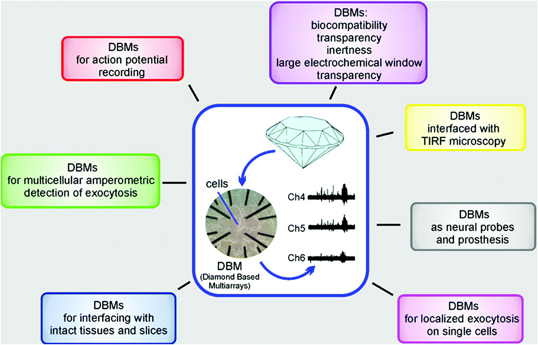 | ||
| Fig. 5 Planar diamond-based multiarrays (DBMs) to monitor neurotransmitter release and action potential firing. Reproduced with permission from ref. 242 and 315. Copyright 2017, American Chemical Society. | ||
4.2 Electrochemical degradation
Ecological degradation or environmental depletion occurs in two ways, by human processing and naturally. The advanced oxidation process (AOP) is one of the most promising, efficient, and environmentally friendly methods of human processing, which has been developed to remove organic pollutants and synthetic dyes from wastewaters.For AOPs, BDD electrodes function as promising anodes to electrochemically degrade environmental pollutants, so-called electrochemical environmental degradation. This is because on BDD electrodes hydroxyl radicals (˙OH) are generated efficiently during AOPs in both acid and neutral media.192,325–329 This radical is a very strong oxidizing species due to its high standard potential (E° = 2.80 V vs. NHE), and is extremely reactive and can be produced in sufficiently high concentrations. Moreover, it reacts non-selectively with most organic pollutants and synthetic dyes via abstraction of a hydrogen atom (dehydrogenation) or addition to a nonsaturated bond (hydroxylation) until total mineralization or conversion into CO2, water, and inorganic ions.192,330,331 Conversely, in both acidic and alkaline solutions, only partial mineralization of most aromatics is realized on conventional AOP anodes (e.g., Pt, PbO2, doped PbO2,332 doped SnO2, and IrO2).
On BDD anodes, further reactions can occur, i.e., the formation of persulfate,333,334 perphosphate and percarbonate,335 and hypochlorite,336–338 which can also be used for wastewater treatment. The synthesis of ferrates, ozone,287,339,340 and aromatic hydroxylation formation mediated by ˙OH radicals produced electrochemically has been reported.341 In addition, BDD possesses several technology essential characteristics such as an inert surface with low adsorption properties, remarkable corrosion stability (even in strongly acidic media) and an extensive potential window in aqueous and non-aqueous electrolytes. Therefore, electrochemical AOP (EAOP) using BDD anodes342–366 has been widely investigated to degrade organic components, especially those in wastewaters.
| H2O → HO˙ + H+ + e− | (1) |
| 2HO˙ → O2 + 2H+ + 2e− | (2) |
The reactivity of the hydroxyl radicals on the electrode surface depends on the electrode material.192 An “active electrode” shows a strong interaction between the hydroxyl radical and the electrode surface, while a “non-active electrode” shows a weak interaction. On “active electrodes”, the adsorbed hydroxyl radicals may interact with the electrode, with the surface changing to a higher oxide (3). Then, the competitive reactions, i.e., the oxidation of organic compounds (4) and chemical decomposition of the higher oxide to form oxygen (5), occur.
| M(˙OH) → MO + H+ + e− | (3) |
| MO + R → M + RO | (4) |
| MO → M + ½O2 | (5) |
On a “non-active electrode”, the interaction between the hydroxyl radicals and the electrode surface is weak. Therefore, hydroxyl radicals are physically adsorbed at the electrode surface. Then the oxidation of organic compounds is mediated only by the hydroxyl radicals (6). In fact, the hydroxyl radicals can discharge to oxygen without any participation of the electrodes (7).
| M(˙OH) + R → M + mCO2 + nH2O + e− | (6) |
| M(˙OH) → M + ½O2 + H+ + e− | (7) |
The BDD electrode is considered to be an ideal non-active electrode, since it has an inert surface of sp3 carbon and its surface has very weak adsorption properties. Consequently, the water oxidation reaction at a BDD electrode in aqueous solution induces the formation of hydroxyl radicals192,325–329 instead of oxygen evolution. Evidence for generation of hydroxyl radicals in aqueous solution at the BDD electrode has been provided using different ex and in situ techniques.192,327
To improve the degradation and complete mineralization of organic pollutants, various combined degradation methods have been developed. As summarized in Table 1, these techniques mainly include the combination of EAOP with Fenton, UV irradiation, ultrasound, microwave, and ozonation.384–389 Here the Fenton method refers to the activation of hydrogen peroxide in acidic effluents.367,368 These combined techniques further enhanced the degradation performance of BDD anodes.390–393 For example, combining ultrasonic oxidation with AOPs led to much enhanced degradation performance towards some non-biodegradable organic pollutants (e.g., alkylphenol ethoxylate surfactants, trichloroethylene, poly n-alkyl acrylates, and phthalic acid esters).370,391,394,395 Ultrasound assisted AOP influenced remarkably the degradation performance toward phenol and phthalic acid, including degradation efficiency, electrooxidation energy consumption, mass transport, and electrochemical reaction. A reduction of the average electrooxidation energy consumption by a factor of 74% and 69% was reported for phenol and phthalic acid, respectively. The mass transport process was also greatly accelerated using ultrasound, as confirmed by a 32% increase of the oxidation peak current for phenol (Fig. 6A).348
| Method | Pollutant(s) | Degradation conditions | Degradation performance | Ref. | |||
|---|---|---|---|---|---|---|---|
| Current/mA cm−2 | T/°C | Parameters | Final products | Removal efficiency (%) | |||
| Electrochemical oxidation | 2,4,5-Trichlorophenoxyacetic acid | 2, 8, 15, 30 | 35 | TOC | CO2 + H2O | 100 | 346 |
| Sodium dodecyl benzene sulfonate | 25–75 | 80–450 | COD | CO2 + H2O | 100 | 347 | |
| Malic acid and ethylenediaminetetraacetic acid | 4 | 41 | COD | CO2 + H2O | 85 to 100 | 344 | |
| Glucose and potassium hydrogen phthalate | 24 | COD, TOC | CO2 + H2O | 90 | 401 | ||
| Atrazine | 25 | TOC | CO2 + H2O | 94 | 402 | ||
| Enrofloxacin | 400 | 35 | TOC | CO2 + H2O | 51 | 403 | |
| 2-Naphthol | 15–60 | COD | 1,2-Naphthoquinone and polymeric materials H2O + CO2 | 100 | 331 | ||
| 4,6-Dinitro-o-cresol | 33–150 | TOC | H2O + CO2 | 85 | 330 | ||
| Fenton oxidation | 2,4-Dichlorophenoxyacetic acid | 100 | 35 | TOC | Formic acid | 79 | 404 |
| DMPO | 23, 160 | 15 | TOC | CO2 + H2O | 100 | 192 | |
| Ultrasound oxidation | Phenol, phthalic acid | 20 | 10 | COD | CO2 + H2O | 79 and 32 | 384 |
| Microwave oxidation | 2,4-Dichlorophenoxyacetic acid | 10 | COD | CO2 + H2O | 46.8–98 | 361 | |
| Azo dye (methyl orange) Platinum anode | 25 | TOC | CO2 + H2O | 78 | 360 | ||
| Ozonation | p-Nitrophenol | 8 | 30 | TOC | CO2 + H2O | 91 | 393 |
| Industrial effluents | 10, 20, 30 | COD | CO2 + H2O | 99.9 | 405 | ||
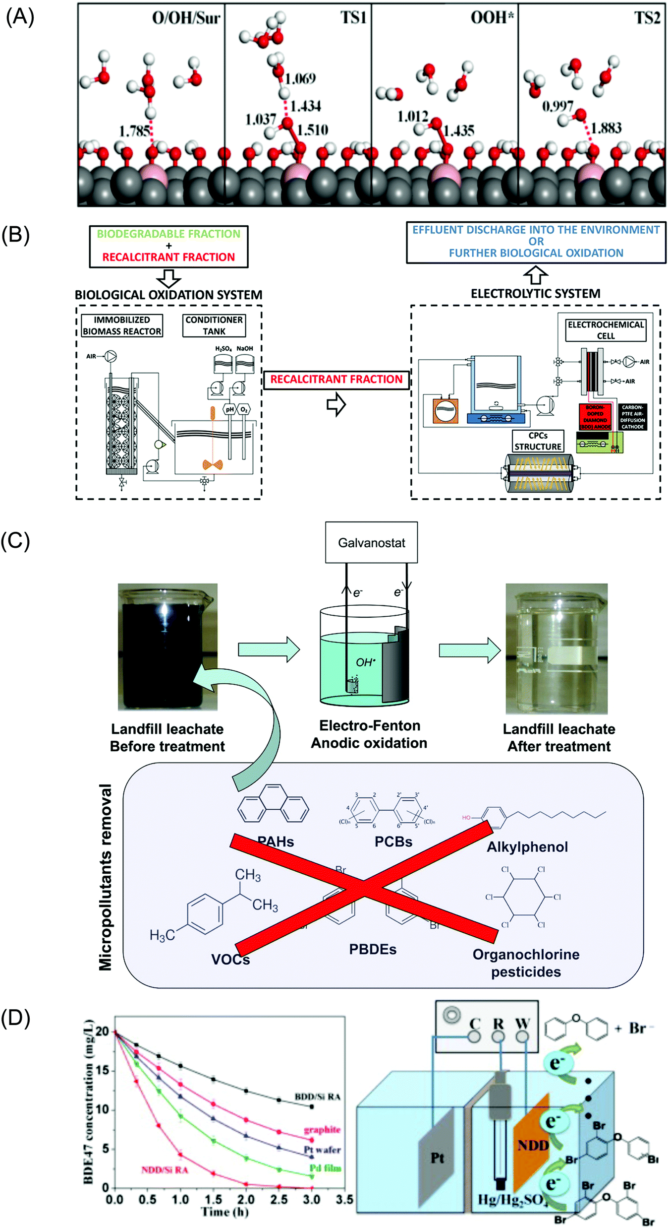 | ||
| Fig. 6 (A) Reaction pathway and mechanism of ultrasonic electrochemical reaction on BDD electrodes. Reproduced with permission from ref. 348. Copyright 2015, John Wiley and Sons. (B) Remediation of a winery wastewater combining aerobic biological oxidation, EAOP, and BDD anodes. Reproduced with permission from ref. 399. Copyright 2015, Elsevier. (C) Occurrence and removal of organic micropollutants in landfill leachates treated by EAOP and BDD anodes. Reproduced with permission from ref. 400. Copyright 2015, American Chemical Society. (D) Nitrogen-doped nanodiamond rod array electrode with superior performance for electroreductive debromination of polybrominated diphenyl ethers. Reproduced with permission from ref. 100. Copyright 2014, Elsevier. | ||
The combination of microwave with EAOP also enhanced the degradation of 2,4-dichlorophenoxyacetic acid and triclosan.360 Increased temperature or mass transport conditions, induced by focused microwaves at a BDD, was thought to be responsible for enhancing the electrochemical oxidation of phenol in aqueous NaOH and NaCl solutions.360,396,397 Ozonation improved EAOP mineralization of p-nitrophenl,392,393 nitrobenzene and m-nitrotoluene.391,398 In aqueous solutions, the TOC removal was up to 91% when a time of 60 min for the electrolysis-ozone process was applied. With the same reaction time, only 20% and 44% of TOC was removed by individual electrooxidation and ozonation treatment.
Using these combined degradation techniques and BDD anodes, EAOP degradation of various organic pollutants (e.g., synthetic dyes) has been reported.406–428 For example, degradation of metribuzin,413,414o-nitrophenol,415 acid violet 7 dye,416 reactive Orange 16,417 a mixture of three pesticides (e.g., chlortoluron, carbofuran, and bentazon),347,388,415,418–420 nitrate,390,421 pharmaceuticals (e.g., ciprofloxacin, sulfamethoxazole, and salbutamol),422 bisphenol A,422–424 fluorinated antidepressant fluoxetine,421 aspirin,330,343,344 caffeine,425 ethidium bromide,426 and Ponceau 4R (Fig. 6B)399,428 has been reported. Safranin T and bromophenol blue have also been degraded. Safranin T was completely removed at a constant current through its reaction with electro-generated hydroxyl radicals.408–410 Fluorinated antidepressant fluoxetine421 was degraded into four aromatic products. Among Pt, RuO2, and BDD anodes, the BDD anode showed the highest mineralization rate due to the fastest production of hydroxyl radicals. For degradation of aspirin using BDD anodes, the degradation mechanism involves both direct and indirect electrochemical oxidation, while there is only indirect oxidation of aspirin on a PbO2 electrode.330
Complete depletion of four hexachlorocyclohexane isomers was confirmed with a mineralization degree of 90% after an electrolysis time of 4 h at a current intensity of 400 mA. Hexachlorocyclohexanes and chlorobenzenes were transformed respectively into chlorinated and hydroxylated intermediates that were rapidly oxidized to non-toxic carboxylic acids.432,433 As confirmed by phototoxicity tests, BDD anodes are useful for reducing the toxicity of hazardous wastewater.411 Compared to the Ti-Ru-Sn ternary oxide anodes, the BDD anode exhibited faster and more efficient maximum COD removal but with less energy consumption for degradation of paper mill wastewater.427 A BDD anode enabled complete COD, colour and ammonium removal after 8 h of electrolysis. When evaluated using COD and DOC, a higher degradation efficiency of bioorganic contaminant wastewater was achieved on BDD anodes in comparison to Ti/Pt–IrO2 and Ti/SnO2–Sb anodes.429–431 Once again, a BDD anode exhibited much better degradation performance in terms of evolution of aromatic compounds, COD, ammonium, colour removal, current efficiency, and energy consumption (Fig. 6C).400,435,440,449–452 The suspension of persistent chromium complexes in wastewater was degraded and almost complete Cr abatement (over 99%) was obtained.453 Efficient degradation of EDTA in the waste solution and the removal of Pb, Zn, and Cd from Sugarcane industries’ pollutants were also investigated with the metals removed via an electrochemical electroplating process. Removal ratios of up to 98.1, 96.1, and 99.1% were obtained for Pb, Zn, and Cd, respectively. The degradation of chelant was up to 99.1%.454 The degradation of THF from industrial wastewaters with an efficiency of up to 95% has also been reported, leading to the statement, BDD anodes have great potential for the practical treatment of industrial wastewaters containing high concentrations of THF.371–373Table 2 lists some examples of EAOP degradation of multiple organic pollutants in real wastewaters.
| Pollutants | Current density/mA cm−2 | Parameters | Final products | Removal efficiency (%) | Ref. |
|---|---|---|---|---|---|
| Hexachlorocyclohexanes | 3.7 | TOC | CO2 + H2O | 90 | 390 |
| 2,6-Dichlorobenzamide | 50 | TOC | CO2 + H2O | 80 | 433 |
| Parabens | 38.97 | TOC | CO2 + H2O | 100 | 434 |
| Surplus ammonia–nitrogen | 20–60 | COD | CO2 + H2O | 60 | 375 |
| Municipal wastewater, human urine, river water, slaughterhouse wastewater | 35.7 | COD | CO2 + H2O | 84–91 | 440 |
| Micro pollutants, humic substances | 21 | TOC | CO2 + H2O | 93 | 400 |
| Pharmaceuticals, pesticides | 9.8–19.6 | COD | CO2 + H2O | 100 | 435 |
| Carbamazepine | 1.8–17.7 | TOC | CO2 + H2O | 52–73 | 455 |
| Municipal solid waste | 20–80 | COD | CO2 + H2O | 35–65 | 411 |
The dopant level and type of diamond anode also influence electrochemical degradation performance towards organic pollutants. For example, EAOP degradation of rubin F-2B,459 enrofloxacin,403 and reactive orange 16460 was more efficient using higher doped than lower doped BDD electrodes. As for the effect of the type of the dopant, Fig. 6D shows one example using a NDD rod array electrode for electroreductive debromination of polybrominated diphenyl ethers.100 Since such an electrode exhibited a low hydrogen evolution potential (−1.95 V vs. Hg/Hg2SO4 electrode), it showed superior activity for electroreductive debromination of the persistent 2,2′,4,4′-tetrabromodiphenyl ether (BDE-47). Over 97% BDE-47 (20 mg L−1) was electrochemically reduced in 2 h at −1.85 V (vs. Hg/Hg2SO4 electrode) with a first-order kinetic constant of 1.93 h−1, which was ×8.7, ×4.7, ×3.5 and ×2.3 greater than that at BDD, graphite, Pt wafer, and Pd film electrodes, respectively, under the experimental conditions applied. Note that although NDD films80,82,100 have been employed as cathodes for the degradation of organic pollutants, the comparison of anodic degradation performance towards organic pollutants using BDD anodes with that using NDD anodes is missing in the literature.
Finally, surface nanostructuring of BDD anodes (e.g., porous diamond,461–463 diamond nanowires,464etc.) enhanced the degradation performance towards organic pollutants. For example, a porous BDD anode was found to be more effective, leading to complete mineralization and rapid degradation of methylene blue.412 In general, porous BDD anodes were more effective at oxidising organic pollutants, leading to complete mineralization, in comparison to planar BDD and PbO2 anodes.461–463 The greater surface area and enhanced mass transfer of the porous BDD anode led to enhanced EAOP degradation of glyphosate and phenol in terms of reaction rate, current efficiency, and energy consumption.409,412
4.3 Electrosynthesis
Electrochemical organic synthesis is considered as a “green” technology for organic synthesis, because only electrons are used as reagents and almost no reagent waste is produced.465 For example, for normal molecular transformations including cleavage of carbon–hydrogen bonds, oxidation or reduction with metal catalysts is necessary. On the other hand, oxidant or reductant free and catalyst free molecular transformations are possible in electrochemical synthesis by precise adjustment of electrochemical parameters such as redox potential, current density, etc. Furthermore, novel reaction chemistry occurring via electrochemically generated intermediates is also possible.Electrochemical synthesis using BDD electrodes shows some advantages in comparison with that using conventional electrodes. This is due to the unique electrochemical properties of BDD electrodes, including the wide potential window and generation of active species such as hydroxyl radicals. Therefore, applications of BDD electrodes in electrochemical synthesis are very promising for novel chemical transformation.22 In this section, electrochemical synthesis applications through anodic oxidation and cathodic reduction reactions are reviewed and discussed.
4.3.1.1 Electrochemical synthesis via methoxy radicals. In 2004, Comninellis et al. reported the first example of an electrochemical reaction via methoxy radicals generated by the anodic reaction of methanol using BDD electrodes. Anodic oxidation of 1,2-diphenyl-ethanes in CH3OH–H2SO4–H2O solution produced p-tert-butylbenzaldehyde dimethyl acetal via carbon–carbon bond cleavage due to the formation of methoxyl radicals.466 Furthermore, trimethylorthoformate production by anodic oxidation of formaldehyde dimethylacetal in solutions containing methanol using BDD electrodes was also reported.467 Electron spin resonance (ESR) was used to confirm generation of the methoxy radicals (Fig. 7).468 Anodic oxidation of methanol containing 0.1 M LiClO4 and 1 mM DMPO (radical trapping agent: 5,5-dimethyl-1-pyrroline-N-oxide) was performed at a constant potential of +1.6 V (vs. Ag/AgCl) using a BDD electrode. The ESR signal of the product mixture showed the magnetic field value anticipated for nitroxyl radicals, which were generated by the reaction of methoxyl radicals with 5,5′-dimethyl-1-pyrroline N-oxide.468 The same experiments using both GC and Pt electrodes showed lower intensities of the ESR signals for the radicals, indicating that methoxyl radical generation was more effective at the BDD electrodes.
 | ||
| Fig. 7 ESR spectra obtained for the methoxy radical on several electrode materials. Standard condition: 10 mM solutions of 5,5′-dimethyl-1-pyrroline N-oxide in 0.1 M LiClO4 dissolved in MeOH, Pt-wire cathode (applied potential: 1.06 V vs. SCE), AN (hyperfine coupling constant of N) value: 13.37 G (cf. 13.58 G), AH (hyperfine coupling constant of H) value: 7.98 G (cf. 7.61 G). Reproduced with permission from ref. 468. Copyright 2012, Wiley-VCH Verlag GmbH & Co. KGaA. | ||
Furthermore, electrochemical oxidation of isoeugenol (1) using BDD electrodes produced benzofuran-type neo-lignan (3: lycarin A), molecule 5, as a result of coupling of the intermediate (2) with the produced methoxy radicals, and molecule 4 as a result of self-coupling of 2 (Scheme 1).468 Recently, anodic methoxylation of 2-oxozolidinone using BDD electrodes has also been reported.469
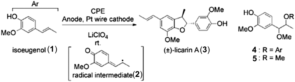 | ||
| Scheme 1 Electrochemical synthesis of licarin A (3). Reprinted with permission from ref. 468. Copyright 2012, Wiley-VCH Verlag GmbH & Co. KGaA, Weinheim. | ||
4.3.1.2 Anodic coupling reactions. Formation of the biaryl skeleton is one of the most important subjects in organic synthesis. Waldvogel et al. reported several examples showing C–H activation reaction and C–C coupling reaction of phenols, arenes, and heterocyclic compounds using BDD electrodes.470–472 In 2006, they demonstrated chemoselective anodic ortho-coupling reaction of 2,4-dimethylphenol. Anodic oxidation using BDD electrodes, under solvent-free conditions, led to very high selective formation of 2,2′-biphenol, with other possible by-products formed only at a trace level.470 Further developments saw improvements in the yield and selectivity of several homo-coupling reactions of phenols in the presence of highly fluorinated alcohols, i.e., 1,1,1,3,3,3-hexafluoroisopropyl alcohol (HFIP).471 In 2010, anodic and selective phenol–arene cross-coupling reactions in HFIP using BDD electrodes (Scheme 2) were developed.472
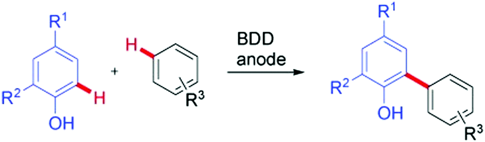 | ||
| Scheme 2 The anodic cross-coupling reactions between phenols and arenes using BDD electrodes. Reprinted with permission from ref. 472. Copyright 2010, Wiley-VCH Verlag GmbH & Co. KGaA, Weinheim. | ||
Furthermore, employing water or methanol as the mediator in solution was found to improve the selectivity and synthetic yields, due to the shift of the oxidation potential.473–475 In addition, partially protected nonsymmetric 2,2′-biphenols were selectively formed with high yields. The anodic reaction of O-silyl-protected phenols produced the desired nonsymmetric 2,2′-biphenols since the use of bulky silyl groups for blocking one hydroxyl moiety prevents the oxidation of the final products (Scheme 3).476 Recently, C–C cross coupling of phenols with thiophenes, that are heterocyclic compounds, has also been reported.477
 | ||
| Scheme 3 General reaction pathway for the anodic synthesis of partially protected nonsymmetric biphenols. PG: protecting group. Reprinted with permission from ref. 476. Copyright 2016, Wiley-VCH Verlag GmbH & Co. KGaA, Weinheim. | ||
Electrochemical oxidation of isoeugenol in HFIP solution using BDD electrodes has also been studied. A stereoselective and electrocatalytic coupling reaction of isoeugenol was observed. The particular C–C bond formation and diastereoselectivity was driven by an interaction between the generated radical species and isoeugenol molecules. It was suggested that the reactant confined in the HFIP solvate cage induced the specific molecular orientation. The reason for the stereoselective conversion was considered to be the solvate interaction between HFIP and the substrate (Scheme 4).478
 | ||
| Scheme 4 Postulated electrocatalytic cycle of the anodic conversion of isoeugenol. Reproduced with permission from ref. 478. Copyright 2018, Royal Society of Chemistry. | ||
 | ||
| Scheme 5 Expected coupling products from one-electron oxidation (left) and one-electron reduction (right) of C6–C3 compounds. Reproduced with permission from ref. 479. Copyright 2015, Beilstein-Institut, Germany. | ||
Electrochemical reduction of ester methyl cinnamate (6) at a constant current in acetonitrile produced 7, 9, and the hydrodimer, dimethyl 3,4-diphenylhexanedioate (8) (Scheme 6)479 Although GC electrodes gave similar products to that of the BDD electrode, Pt and Mg electrodes showed mainly hydrogen evolution. The hydrodimer (8) was then successfully converted by chemical reactions to neolignan-type compounds.480
 | ||
| Scheme 6 Electrochemical reduction of ester methyl cinnamate (6) using a BDD electrode. Reproduced with permission from ref. 479. Copyright 2015, Beilstein-Institut, Germany. | ||
The following facts have been thus established for electrosynthesis using BDD electrodes:22 (i) BDD electrodes are required with low NDC content and high conductivity (BDD with high boron levels); (ii) no effect of BDD surface termination on electrosynthetic applications has yet been found; (iii) initiation of electrochemical reactions occurs only after the formation of oxyl radicals; (iv) there are no advantages of BDD electrodes over other electrodes unless radical compounds are formed; (v) the wide potential window of BDD electrodes plays a key role and determines the selectivity of the products; (vi) the applied current or potential is crucial for product selectivity.22
4.4 Electrocatalysis
BDD and NDD films have been employed as electrodes or catalyst support for electrocatalytic applications. For example, electrochemical and photoelectrochemical reduction of carbon dioxide, a hot topic in the field of electrocatalysis,481–487 has been conducted using conductive diamond as a metal-free electrocatalyst (also named carbocatalyst).384 Conversely, loading of metal catalysts onto the surface of conductive diamond has expanded the usage of diamond films in fuel cells.Several reports have been published concerning the utilization of conductive diamond for CO2 reduction. For example, on undoped diamond with hydrogen termination, reduction of aqueous CO2 to CO was achieved with a product selectivity of greater than 90% (Fig. 8A). The radicals of CO2˙− were produced by solvated electrons through illumination of inexpensive diamond substrates with UV light.488 Later, hydrogen-terminated diamond NPs with an average diameter of 125 nm were employed to initiate selective photochemical reduction of CO2 to CO.489
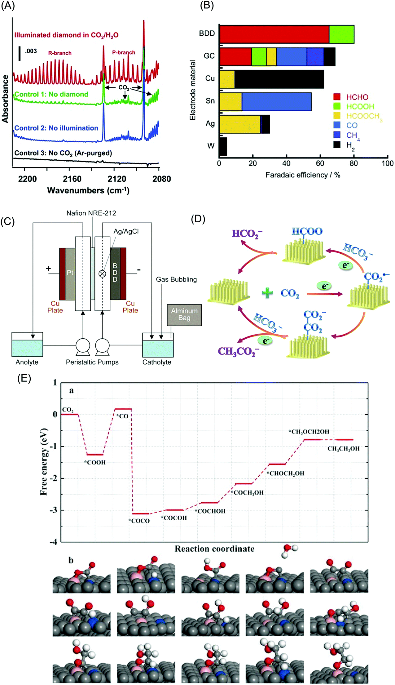 | ||
| Fig. 8 (A) FTIR spectra of gaseous head space demonstrating reduction of CO2 to CO by illuminated diamond, along with control samples. Reprinted with permission from ref. 489. Copyright 2014, Wiley-VCH Verlag GmbH & Co. KGaA, Weinheim. (B) Faradaic efficiency of the products generated by the electrochemical reduction of CO2 using various electrodes in a MeOH electrolyte. The electrochemical reduction was performed at −1.5 V (vs. Ag/Ag+) using a platinum counter electrode in a two-compartment cell (100 mL) separated by Nafion for 1 h at room temperature and atmospheric pressure. Reprinted with permission from ref. 482. Copyright 2014, Wiley-VCH Verlag GmbH & Co. KGaA, Weinheim. (C) Diagram of the two-compartment flow cell. Reprinted with permission from ref. 491. Copyright 2018, Wiley-VCH Verlag GmbH & Co. KGaA, Weinheim. (D) Schematic pathway for electrocatalytic CO2 reduction on a N-doped nanodiamond coated Si rod array electrode. Reprinted with permission from ref. 497. Copyright 2015, American Chemical Society. (E) (a) Free energy diagrams for CO2 reduction on the (111) facet of boron- and nitrogen-co-doped diamond (BND), (b) energetically favorable structures for elementary steps of CO2 reduction on the (111) facet of BND (gray = C, pink = B, blue = N, red = O, white = H). Reprinted with permission from ref. 63. Copyright 2017, Wiley-VCH Verlag GmbH & Co. KGaA. | ||
Other conductive (doped) diamond electrodes have also been employed for electrochemical CO2 reduction. On BDD electrodes, electrochemical reduction of CO2 in methanol containing tetrabutylammonium perchlorate (TBAP) was found at a potential of −1.5 V (vs. Ag/AgCl), with hydrogen evolution commencing at a potential of around −1.8 V (vs. Ag/AgCl). Under a potential of −1.5 V (vs. Ag/AgCl), the main products were formaldehyde and formic acid. In comparison to other electrodes (e.g., GC, Cu, Sn, Ag, W), their yield efficiencies using BDD were the highest (Fig. 8B). It was explained that BDD with its sp3 carbon bonds functions as an ideal “non-active electrode” known to have lower adsorption properties. The radical CO2˙− was possibly formed, followed by the formation of formaldehyde or formic acid.482 Such mechanisms were further elaborated by Koper et al., who discussed the importance of disproportion and chemical reaction including base-catalysed Cannizzaro reactions.490
The performance of BDD electrodes towards CO2 reduction (e.g., faradaic efficiency, product selectivity, etc.) was further improved through optimization of solution composition (e.g., alkali-metal cations,491 ammonia solution as the absorber492,493) and the effect of boron-concentration494,495 was further conducted. When a flow cell system was applied (Fig. 8C), a faradaic efficiency for the production of formic acid as high as 94.7% was obtained with a rate of production up to 473 μmol m−2 s−1.491 BDD was also decorated with a catalytically active cobalt complex for electrochemical CO2 reduction. Such surfaces exhibited good stability and electrocatalytic activity toward electrochemical reduction of CO2 to CO in acetonitrile solution.496 Silver NP coated oxygen-terminated BDD films showed excellent selectivity for photoelectrochemical CO2 reduction into CO (e.g., estimated CO:H2 mass ratio of 318:1) and recycling ability (e.g., stable for five cycles of 3h each) under 222 nm irradiation.480 Furthermore, copper-modified BDD electrodes were able to produce C2 and C3 species (e.g., ethanol, acetaldehyde, and acetone) at a relatively low potential (−1.0 V vs. Ag/AgCl).493
On a nitrogen-doped nanodiamond coated Si rod array, CO2 was preferentially and rapidly converted to acetate over formate with an onset potential of −0.36 V (vs. RHE). A faradic efficiency of 91.2–91.8% was achieved for CO2 reduction at −0.8 to −1.0 V. Such superior performance for CO2 reduction was attributed to its high overpotential for hydrogen evolution and nitrogen doping, where N-sp3 carbon species were highly active for CO2 reduction. Electrokinetic data and in situ infrared spectrum revealed the main pathway for CO2 reduction as CO2 → CO2˙− → (COO)2˙ → CH3COO− (Fig. 8D).497 On the other hand, on the boron and nitrogen co-doped nanodiamond (BND) electrode, efficient, stable, and selective reduction of CO2 to ethanol was achieved with a high Faradaic efficiency of 93.2% at −1.0 V (vs. RHE). The synergistic effect of boron and nitrogen co-doping, high nitrogen content and high overpotential for hydrogen evolution were proposed to explain such a superior performance. The possible pathway for CO2 reduction revealed by DFT computation (Fig. 8E) was suggested as CO2 → *COOH → *CO → *COCO → *COCH2OH → *CH2OCH2OH → CH3CH2OH.63
In conclusion, various conductive diamond films and structures are useful for electrochemical energy conversion. Their surface chemistry as well as dimensions determines the catalytic performance for these energy storage applications.
4.5 Electrochemical energy storage
Due to the unique advantages of BDD (e.g., wide electrochemical potential window, varied surface termination, high mechanical hardness, high thermal conductivity, chemical inertness, excellent stability in various harsh environments and under extremely tough conditions, etc.),503 it has been utilized recently as an electrode material to construct various electrochemical energy storage devices (e.g., supercapacitors, batteries, solar cells, etc.).000000 charging–discharging cycles), wider ranges of operating temperatures (from −40 to 70 °C), and better safety.504 In other words, SCs own higher energy densities than conventional capacitors and much larger power densities compared to batteries. According to the charge storage mechanisms, SCs can be classified into two types: electrical double layer capacitors (EDLCs) based on ion adsorption/accumulation at the interface of the electrode and the electrolyte and pseudocapacitors (PCs), which rely on reversible faradaic reactions of redox species immobilized on the electrodes or dissolved in the solution. The performance of a SC is generally evaluated by four physical parameters: capacitance (C), power (P) and energy densities (E), as well as the cycling stability (or capacitance retention). The development of high performance SCs, namely those with high and stable C as well as high E and P, is the core of SC research for both science and industry. Nowadays, the applications of SCs have been expanded to a variety of areas, ranging from low-emission hybrid electric vehicles, pulse power sources, to backup sources for high power delivery or uptake. Moreover, flexible, printable, and wearable SCs have been integrated as well into smart clothes, sensors, wearable electronics, and drug delivery systems.505–508
To improve the capacitance of conductive diamond SCs, producing diamond electrodes with large surface areas is a promising and efficient approach. Moreover, conductive diamond has a rich surface carbon chemistry and varied surface terminations. Therefore, besides acting as a capacitor, BDD can be integrated with other sp2 carbon materials to form hybrid films. Such diamond-based films are expected to deliver much higher capacitances than BDD itself. Additionally, through the combination of diamond-based nanostructures with redox species loaded onto the electrode or dissolved in the solution, PCs with enhanced performance have been fabricated. The performance of SCs based on various conductive diamond nanostructures and different electrolytes is shown in Fig. 9.
 | ||
| Fig. 9 (A) Comparison of capacitances of conductive diamond SCs. (B) Comparison of power and energy densities of battery-like conductive diamond SCs with capacitors, electrochemical capacitors and batteries. Reprinted with permission from ref. 509. Copyright 2018, University of Siegen, Siegen, Germany. | ||
4.5.1.1 Conductive diamond EDLCs. Various porous nanostructures (e.g., diamond paper,94 honeycomb diamond,95 porous diamond,96 diamond nanowires,97etc.) (Section 2.3) have been applied as capacitor electrodes for the construction of EDLCs. In most cases, a three-electrode system was employed to estimate the capacitances of these capacitor electrodes. The comparison of their capacitances is shown in Fig. 9(A).509 For example, a honeycomb structured BDD based EDLC showed a specific capacitance of 3910 μF cm−2 and 666 μF cm−2 in aqueous and organic solution, respectively.510 A roughened BDD surface layer with excavated holes was produced by catalytic dissolution of the carbon structures with nickel, cobalt, and platinum NPs in a hydrogen atmosphere under a high temperature. This procedure resulted in a larger surface area and thus the capacitance of this BDD electrode was ×15 enhanced in comparison to that of a planar diamond electrode.511
Diamond foam based EDLCs, produced via overgrowth of SiO2 spheres with thin BDD films, attained specific capacitances of 598 and 436 μF cm−2 in aqueous and organic solutions, respectively, as well as a high power density of 807 W cm−3. These diamond foam based EDLCs are close to producing the best power performance of electrolytic capacitors.512 The capacitance of a BDD (with a thickness of 240 nm) coated silicon nanowire structure was 105 μF cm−2 in the ionic liquid 1-methyl-1-propylpyrrolidinium bis(trifluoro methylsulfonylimid). An energy density of 84 μJ cm−2, a power density of 0.94 mW cm−2, and good stability (retention stability of 93.3% after 10000 cycles at the scan rate of 5 V s−1) were demonstrated.513 An alternative porous BDD structure produced using a highly porous polypyrrole scaffold as the template exhibited a capacitance up to 3 mF cm−2 in aqueous LiClO4 and a low electrochemical impedance. At low frequency, between 0.1 Hz and 10 Hz, the impedance of the electrode with an area of 0.12 cm−2 was measured to be ×600 lower than that of a planar diamond electrode.514
Porous BDD films overgrown on CNTs showed about ×450 enhancement in the electro-active area and double-layer capacitance in comparison to that for a planar BDD electrode.515 BDD films grown on carbon fibers obtained from poly-acrylonitrile precursors through heat treatment at 2000 °C delivered an increased capacitance of up to 1.94 mF cm−2. This value is about ×8 larger than that for carbon fibers formed under identical conditions.516 By combining conductive diamond with these sp2 carbon materials, enhanced performance has been achieved, compared to that of BDD EDLCs alone. This is attributed partially to further increased surface areas and partially to the addition of the capacitances from the other carbon materials.417 Porous BDD formed by means of a two-step thermal etching of diamond showed a capacitance of 140 μF cm−2 in aqueous solution.90 A diamond porous structure obtained via the oxidative etching of BDD electrodes with steam or CO293 improved its active surface area by a factor of 20 compared to a planar BDD.91 The capacitance of a porous conductive diamond network was recorded to be 13.7 F g−1 or 17.3 F cm−3 at 0.1 V s−1 in 0.1 M H2SO4.89 These values are comparable to that (ca. 13 F g−1) of a BDD hollow fiber.517
Due to the rich carbon surface chemistry, BDD is also promising as the electrode support to form novel sp2–sp3 carbon hybrid films. For example, the direct growth of other sp2 carbon materials (e.g., CNTs,518 graphene,519 carbon nanofibers (CNF),520etc.) on thin BDD films has been studied. For example, hybrid films of vertically aligned CNFs on BDD (CNF/BDD) have been grown in a thermal CVD reactor; a sputtered copper thin film acted as the catalyst and C2H2 as the reaction gas. In 1.0 M H2SO4 aqueous solution, the capacitance of a CNF/BDD based EDLC was as high as 137.90 mF cm−2 at a current density of 2 mA cm−2.520 Such a large capacitance is due to the following factors: (i) a large surface area of this CNF/BDD hybrid film due to its porous structure, (ii) high conductivity due to containment of stacked graphene layers inside CNFs and copper metal catalysts inside the CNFs, (iii) high stability, and (iv) free of binder.
Conductive diamond particles (Section 2.4) have been applied for the construction of supercapacitors. They are normally annealed at high temperature under vacuum or in an inert atmosphere to form onion-like carbon on the nanodiamond surface.521 The capacitances of the EDLCs based on these materials were thus found to be dependent on the degree of diamond graphitization, or annealing temperature.522 For example, through graphitization of DND powder at 897–1867 °C, onion-like carbon with varied structure and properties (e.g., surface area and conductivity) was produced.522 The double layer capacitance was estimated to be about 20–40 F g−1 and 70–100 F g−1 in 1.0 M H2SO4 acid and 6.0 M KOH alkaline solutions, respectively.522 By annealing the composite films of graphene oxide and nanodiamond at 1200 °C, mesoporous graphene and onion-like carbon were synthesized.521 These films were flexible, mechanically stable, and highly conductive (7400 to 20300 S m−1), and exhibited a maximal specific surface area of about 420 m2 g−1 with pore size in the range of 2–11 nm. The formed EDLCs showed a specific capacitance of 143 F g−1 at a discharge current density of 0.2 A g−1 in 1.0 M H2SO4 aqueous solution.521 Furthermore, reduced graphene oxide matrices with intercalated conductive diamond particles of different densities have been prepared and further utilized as electrode materials for SC applications. The reduced mass ratio of graphene oxide to nanodiamond from 10 to 1 provided the maximal capacitance of 186 ± 10 F g−1 in 1 M H2SO4 with excellent cycling stability.523
4.5.1.2 Conductive diamond PCs. To construct conductive diamond PCs, BDD films with different doping levels were deposited on TiO2 (BDD/TiO2) nanotubes and applied as capacitor electrodes.524 The measured capacitances of these capacitor electrodes in 0.1 M NaNO3 at a scan rate of 10 mV s−1 were 2.10, 4.79, and 7.46 mF cm−2 when the concentration ratio of boron to carbon was 2000, 5000, and 10
000, respectively.525 The enhanced performance of the BDD/TiO2 nanotube electrodes was explained by the increased surface area, additional capacitance introduced with the presence of TiC and Ti2O3, the synergistic effect of TiO2 treatment in CH4:H2 plasma and the high electrical conductivity of BDD.525
A more efficient approach to achieve high capacitances of conductive diamond PCs is to use pseudo-capacitive species (e.g., metal oxides, conducting polymers, soluble redox-active couples, etc.) combined with BDD as electrodes or dissolved in the aqueous solutions as electrolytes. For instance, the combination of BDD and RuOx·nH2O for the construction of SCs has been reported. RuOx·nH2O was deposited electrochemically on the BDD film as well as on diamond powders. The specific capacitances obtained in 0.5 M H2SO4 were 132 and 324 F g−1 for the BDD film and powders, respectively.503 Ni(OH)2 decorated conductive diamond nanowires have been employed to construct PCs. Due to the reversible redox transitions of nickel hydroxide and nickel oxy-hydroxide groups, a high gravitational C of 1601 F g−1 (about 80% of the theoretical value) and a P of up to 3 × 10⁵ W kg−1 have been achieved. This high P was explained by the fast ion diffusion inside this 3D composite. However, relatively poor cycling stability was noticed (e.g., the capacitance retained only 70–80% of the initial value after 1000 cyclic voltammetry cycles within a 0.5 V potential window at a scan rate of 100 mV s−1).526
MnO2 coated BDD showed varied capacitances as a function of the mass of MnO2 deposited. At a MnO2 area density of 24 μg cm−2, a maximum C of 326 F g−1 (namely 7.82 mF cm−2) or 349 F g−1 was obtained from CV at a scan rate of 10 mV s−1 or a galvanostatic charging–discharging process at 3 A g−1, respectively. The capacitance retention was only 66% after 1000 charging–discharging cycles at a scan rate of 100 mV s−1.153 The PC based on conductive diamond NPs embedded in polyaniline (with the weight ratios of 3–28%) showed a stable capacitance of 640 F g−1 in 1.0 M H2SO4 for 10000 cycles. This capacitance was ×3–4 higher than that for activated carbons, and more than ×15 higher than that for onion-like carbon.527
As an alternative approach, water-soluble redox couples (e.g., Fe(CN)63−/4−) dissolved in 1.0 M Na2SO4 aqueous solution were used as redox electrolytes to form planar BDD, BDD networks as well as CNF/BDD PCs. For example, when a BDD film was employed as the capacitor electrode, its C reached 41.51 mF cm−2 at a scan rate of 10 mV s−1.528 For the BDD network capacitor electrode, its C was 73.42 mF cm−2 at a charging–discharging current density of 1 mA cm−2.528 By applying a CNF/BDD hybrid film produced under optimal conditions (e.g., a copper sputtering time of 60 s, a CNF growth time of 60 min in a C2H2 atmosphere using a thermal CVD technique) a C of 232.01 mF cm−2 was achieved at a charging–discharging current density of 2.0 mA cm−2.520
Conductive diamond SC devices fabricated with two-electrode configurations have also been reported. The prototype SC demonstrated in an aqueous electrolyte a gravimetric C of 0.688 mF cm−2 (0.645 F g−1) per layer with excellent stability (92% of capacitance retention after 20000 cycles at a current density of 1 mA cm−2).94 A high specific P of 1 × 10⁵ W kg−1 has been achieved as well.94 By applying poly(3,4-(ethylenedioxy)thiophene) (PEDOT) coated BDD diamond overgrown on silicon nanowires as electrodes, the constructed symmetric micro-SC device exhibited a high C of 9.5 mF cm−2, as well as high E and P values of 26 mJ cm−2 and 1.3 mW cm−2 in a large cell voltage of 2.5 V. The capacitance retention was examined to be 80% after 15000 galvanostatic charging–discharging cycles at a current density of 1 mA cm−2.97 When the redox species (Fe(CN)63−/4−) was introduced in the electrolyte, several two-electrode symmetric SC devices have been constructed using planar diamond, diamond network, and CNF/BDD hybrid films as the capacitor electrodes.528 For example, for a diamond PC device, the maximal E and P reached 46.96 W h kg−1 and 9.87 kW kg−1, respectively,528 which increased to 56.5 W h kg−1 and 13.7 kW kg−1, respectively, for a diamond network PC device528 and were found to be 44.1 W h kg−1 and 25.3 kW kg−1, respectively, for a CNF/BDD PC device. A CNF/BDD EDLC device using an inert electrolyte (H2SO4) recorded maximal E and P values of 22.9 W h kg−1 and 27.3 kW kg−1, respectively.520 The performance comparison of these battery-like diamond SCs with capacitors, batteries, and related devices is summarized in Fig. 9B.509
4.1.5.3 Supercapacitor demonstrators. Considering the practical applications, a conductive diamond-based pouch cell was fabricated as a prototype for diamond SCs (Fig. 10A).94 The dimension of the pouch was 1.5 × 2 cm2 using stainless steel as a current collector. Freestanding conductive diamond paper (Section 2.4) was used as the electrode material. Two membranes with the size of the pouch were integrated in the cell. The porous conductive diamond paper (weight only 3.2 mg) was used as the anode. Aqueous 3 M NaClO4 was used as the electrolyte.
 | ||
| Fig. 10 (A) Photos of (a) a piece of free-standing diamond paper with a thickness of ∼50 μm; (b) a diamond pouch cell supercapacitor composed of two pieces of such membranes. The logo of the institute is intentionally blurred for copyright reasons. Reprinted with permission from ref. 94. Copyright 2016, American Chemical Society. (B) A stand-alone CNF/BDD SC demonstrator: (a) a photograph of the demonstrator consisting of three CNF/BDD EDLC devices in series, a single-board microcontroller connected to the computer with a USB cable, and a red LED; (b) the design of a CNF/BDD SC prototype used in the system; (c) the schematic electrical circuit diagram related to (a); (d) typical curves of the voltage as a function of time during the charging–discharging processes. The insets show the variation of light intensity of the red LED in relation to the cell voltage. Reprinted with permission from ref. 520. Copyright 2018, Wiley-VCH Verlag GmbH & Co. KGaA. | ||
A stand-alone demonstrator based on CNF/BDD EDLC devices has also been fabricated (Fig. 10B).520 It consists of three EDLC devices assembled in series, a single-board microcontroller to control the charging–discharging processes, a red light-emitting diode (LED), and a universal serial bus cable to charge the device. In a CNF/BDD SC device, two CNF/BDD capacitor electrodes were attached tightly to both sides of the cell. The area of each electrode exposed to the electrolyte was about 0.785 cm2. A 50 μm Nafion membrane was fixed with two sheets in the middle of the cell and an electrolyte of 1.0 M H2SO4 was employed. With a high voltage at an initial stage, the LED was very bright. The light lasted for a few seconds and became weaker till it ceased.520
Nanodiamonds were used as an electrolyte additive in the presence of lithium ions, in order to produce dendrite-free lithium metal deposits: dendritic growth of Li is a problematic failure mechanism in battery operation. The uniform formation of lithium arrays in the presence of the nanodiamond was postulated due to Li+ ions preferentially adsorbing onto the nanodiamond surfaces with a low diffusion energy barrier. This behavior (Fig. 11A) significantly altered the subsequent lithium plating, resulting in an enhanced electrochemical cycling performance. The nanodiamond-modified electrolyte was found to lead to a stable cycling of lithium|lithium symmetrical cells up to 150 and 200 h at 2.0 and 1.0 mA cm−2, respectively (Fig. 11B).532
 | ||
| Fig. 11 (A) Morphology of Li deposits after galvanostatic plating. Schematic illustration describing Li ion plating behavior in the LiPF6-EC/DEC electrolyte without (a) and with (f) nanodiamond additives. SEM images of (b–e) Li deposits in the LiPF6-EC/DEC electrolyte without the nanodiamond additive. SEM images of (g–j) Li deposits in the LiPF6-EC/DEC electrolyte with nanodiamond additives. (b–d) and (g–i) Li plating after one time at 0.5 mA cm−2 and with plating time of 6 h. (e and j) Li plating after three cycles at 0.5 mA cm−2 and with each step time of 6 h. The insets in (e and j) are the optical images of the corresponding Li deposits. The scale bars in (b and g), (c and h), (d and i), and (e and j) are 100, 1, 50, and 5 μm, respectively. The scale bars in the insets of (b, g, e, and i) are 1 μm. The word ‘‘ND’’ in the figure is the abbreviation of “nanodiamond”. Reprinted with permission from ref. 532. Copyright 2017, Nature Publishing Group. (B) Long-term electrochemical cycling stability. Charge–discharge curves of symmetrical Li|Li cells at (a) 1 mA cm−2 and (b) 2 mA cm−2. Each charge and discharge time is set as 12 min. (c) Voltage–time curves to calculate the average Coulombic efficiency of Li|Cu cells at 0.5 mA cm−2. (d) The enlarged view of (c) from 5 to 15 h. The morphology of a Li deposit cycled at 0.5 mA cm−2 in the electrolyte (e) without and (f) with the nanodiamond additive. The scale bars in (e and f) are 10 μm. The word “ND” in the figure is the abbreviation of “nanodiamond”. Reprinted with permission from ref. 532. Copyright 2017, Nature Publishing Group. (C) An ultrastrong double-layer nanodiamond interface for stable lithium metal anodes: schematic plots of experimental steps, simulated defect-tolerant vs. uniform ion flex, and high strength vs. dendrite suppression. Reprinted with permission from ref. 533. Copyright 2018, Cell Press. (D) Electrochemical characterization of the nanodiamond interface. (a) The electrochemical impedance spectra of bare Cu, DND, and DND–polymer electrodes. (b) The CE of different anode architectures cycled at a current density of 0.5 mA cm−2 and a capacity of 1 mA h cm−2. (c) The CE of bare Cu and DND–polymer electrodes cycled at varying current densities and capacities. (d) Summary of the 10-cycle average CE of the DND–polymer electrode measured according to the method developed by Aurbach et al.534 (e) Long-term cycling CE of bare Cu and DND–polymer electrodes at a current density of 1 mA cm−2 and a capacity of 2 mA h cm−2. (f) Cycling performance of the prototypical Li–S cells at 0.5C with 25 mm Li foil (ca. 5 mA h cm−2), bare Cu with 5 mA h cm−2 electrodeposited Li, or DND–polymer with 5 mA h cm−2 electrodeposited Li as the anode. The areal mass loading of the S cathode is 1.5 mg cm−2. The rate is calculated based on the theoretical capacity of S, where 0.5C is equivalent to 1.25 mA cm−2. Reprinted with permission from ref. 533. Copyright 2018, Cell Press. | ||
A high-quality DND thin film was also developed as an interfacial protection layer to reinforce the native solid–electrolyte interphase on a Li metal anode. A unique double-layer nanodiamond design was proposed to enhance the defect tolerance of the artificial interface, ensuring the macroscopic uniformity of the lithium ion flux. The nanodiamond thin film possessed a hardness of higher than 200 GPa modulus for dendrite suppression (Fig. 11C). Significantly improved battery performance was realized in both half and Li–S full cells, which effectively arrested dendrite propagation, resulting in controlled Li deposition and significantly improved cycling efficiency (Fig. 11D).533
Intrinsic diamond has been proposed as a promising alternative for the development of nuclear batteries, due to its wide band gap (5.5 eV), high radiation resistance, excellent electronic properties, etc. For instance, a nuclear microbattery prototype with an active area of 15 cm2 was fabricated, consisting of 130 single cells based on a Schottky barrier diamond diode. The conversion efficiency of each cell was found to be 4–6%.535 The performance of the microbattery was characterized using different radioisotope sources (e.g., 63Ni, 147Pm, 90Sr–90Y, and 238Pu). By applying a 63Ni source, the battery exhibited a high energy density of 120 W h kg−1 and a total efficiency of only 0.6%. Under irradiation of a 90Sr–90Y source, the battery prototype was found to be stable during 1400 h of radiation exposure.535
4.6 Other applications
BDD electrodes have been employed to develop a novel co-reactant-free electrogenerated chemiluminescence (ECL) system where Ru(bpy)32+ emission was obtained with an in situ generated co-reactant. This method is based on the promoted conversion of inert SO42− into the reactive co-reactant S2O82− on BDD electrodes at very high oxidation potentials in aqueous solutions. The method is straightforward and does not require any particular electrode geometry.540 Significant enhancement of the ECL signals from Ru(bpy)32+ in the presence of tripropylamine was achieved using a BDD nanograss array electrode. This is mainly because of the highly facile oxidation of co-oxidant in the presence of Ru(bpy)32+, resulting from the superior properties of the BDD nanograss array (e.g., improved electrocatalytic activity and accelerated ET kinetics).541Several new integrated techniques have been developed in combination with BDD electrodes, such as electrochemical-spectroscopy,542–545 thermal-electrochemical techniques,546 and BDD platforms for transmission electron microscopy (TEM) – electrochemistry.547 Many of these adopt a free standing (unsupported) BDD film. In the first area, electrochemical X-ray fluorescence (EC-XRF)542 and electrochemistry-UV-vis-IR544,545 methodologies have been advanced. As an example of combining the power of two technologies in the electrochemical-spectroscopy area, EC-XRF was used to electrochemically preconcentrate soluble heavy metals directly onto the surface of a BDD electrode, in a metallic form, for electrochemical interrogation by the XRF.542 In this way chemical identification and quantification of heavy metal concentrations (e.g., Ni, Cu, Zn, Hg, and Pb) directly in solution (Fig. 12A)542 was proven.
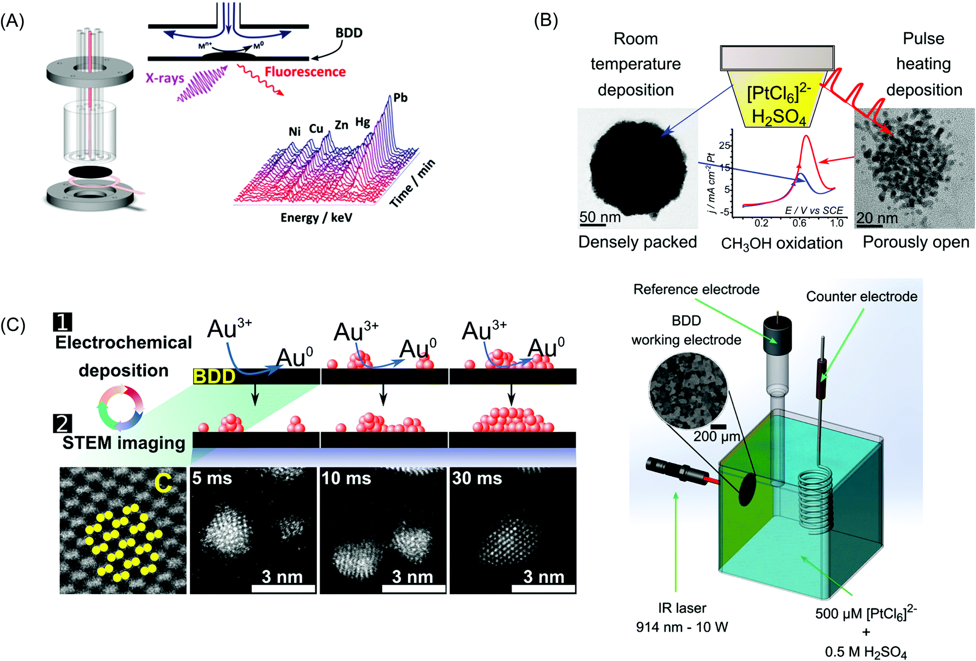 | ||
| Fig. 12 (A) Schematic illustration of direct identification and analysis of heavy metals in solution by use of in situ EC-XRF. Reprinted with permission from ref. 542. Copyright 2015, American Chemical Society. (B) Electrochemical synthesis of nanoporous platinum NPs for methanol oxidation using laser pulse heating (top) and schematic drawing of the pulsed laser heating experimental setup (bottom). The laser beam is focused by the laser lens onto the back face of the BDD electrode held in the Perspex cell with Kapton tape, which also defines the active electrode area (1 mm disk). The inset image is an FE-SEM image of the BDD electrode surface, where the different colours represent the differently doped grains. Reprinted with permission from ref. 543. Copyright 2017, American Chemical Society. (C) Tracking metal electrodeposition dynamics from nucleation and growth of a single atom to a crystalline NP using identical location scanning transmission electron microscopy (STEM) where BDD served as both an electron-transparent TEM substrate and electrode. Reprinted with permission from ref. 547. Copyright 2018, American Chemical Society. | ||
Using an IR laser to locally heat a freestanding BDD film enables local control of the interfacial temperature of a BDD electrode. Temperatures in excess of 100 °C could be generated at the electrode–electrolyte interface, importantly under controlled (non-turbulent) mass transport conditions.548 This approach enabled the study of the effect of temperature on the electrodeposition of metal nanostructures (Pb/PbO546 and Pt543). For example, laser heating was shown to significantly increase the porosity of electrodeposited Pt NPs, which in turn increased the electrocatalytic activity of these nanostructures, towards oxidation of methanol – an important fuel cell component (Fig. 12B).543
Finally, by producing electron transparent TEM plates from BDD it is possible to follow the morphological dynamics of an electrochemical process, at the level of a single atom. For the proof-of-concept study, the BDD-TEM platform was used to investigate the early stages of electrochemically driven nucleation and growth of a single metal atom to a crystalline metal NP (Fig. 12C).547 Here an identical-location approach was employed whereby after an initial growth period, the BDD-TEM plate was removed from solution and imaged at atom-level resolution in the TEM. The platform was then placed back into solution and growth reinitiated. After removal from solution, imaging again took place in the same location as before, and the process was repeated. This procedure thus allowed the growth process to be followed, in the same area, in a series of “time-stamped” images. The use of BDD as the TEM grid, compared to conventional sp2 carbons, was found to offer significant advantages including inherent robustness for repeat measurements, low atomic number, crystallinity, stability, extremely high thermal conductivity and very low Bremsstrahlung backgrounds.
5. Electrochemical devices
In this section, the fabrication of small-dimensional BDD electrodes274–284 as well as their ensembles and arrays,302–311,313,314,317,318,549–551 and scanning probes are summarized.5.1. Micro- and ultramicroelectrodes
Conductive diamond MEs and UMEs have been fabricated by means of conformal BDD layers on small-diameter metal wires, overgrowing diamond layers on lithographically patterned substrates, or oxygen-based ion beam plasma etching of the bulk conductive diamond material.235,280–283 Among them, one frequently applied approach is to coat, by CVD growth, sharpened metal wires with a thin BDD film. The used metals are mainly tungsten (Fig. 13A)274–279 and platinum.235,280–283 Focused ion beam (FIB) milling can be further applied to improve the exposure areas of the disc-shaped MEs (Fig. 13A).279 However, FIB exposure of BDD MEs unavoidably implants Ga+ ions into the BDD electrode surface as well as the amorphisation of BDD surface layers down to several tens of nanometers.552 | ||
| Fig. 13 (A) A BDD microsensor. The left panel shows a scanning electron microscopy image of the microsensor tip. The centre and right panels show a stereo-microscope photograph of a microsensor and a schematic illustration, respectively. Reproduced with permission from ref. 235. Copyright 2017, Nature Publishing Group. (B) (a) Photograph of an integrated all-diamond ultramicroelectrode array chip. The yellow parts are metal contacts. The dark part with a semicircle is the counter electrode, the dark rectangle is the quasi-reference electrode, and the central circle is the working electrode. (b) Schematic plot of the structure of the electrode. (c) Arrangement of the array which is composed of 45 ultramicroelectrodes (10 μm in diameter) in a 500 μm (diameter) circle. Reprinted with permission from ref. 553. Copyright 2011, American Chemical Society. | ||
These MEs and UMEs have been characterized with various techniques such as scanning electron microscopy, optical microscopy, Raman spectroscopy, and electrochemical techniques (e.g., voltammetry, impedance).274–283 On BDD MEs, low and stable background currents were obtained.279,280 At low scan rates, the cyclic voltammograms for redox probes (e.g., Ru(NH3)63+/2+, Fe(CN)63−/4−, etc.) are sigmoidally shaped, as expected. Electrochemical characterization of BDD UMEs by means of cyclic voltammetry also revealed that the porosity of the film (namely when the BDD grains don’t form a contiguous film over the surface of the metal wire tip) affects deleteriously the performance and lifetime of BDD UMEs.279 EIS has also been applied to investigate the size effect of diamond MEs on their electrochemical properties.312 By reducing the size (or diameter) of BDD ME/UMEs, formed from UNCD, from 250 μm to 10 μm, the shape of the Nyquist plots changed from linear lines to two arcs,312 corresponding to the grains of UNCD and grain boundary phases.312
5.2. Micro- and ultramicroelectrode arrays
Various diamond MEAs, UMEA, and NEAs have been fabricated. For example, in 2002, Fujishima and coworkers used structured silicon substrates to fabricate BDD MEAs,550 which consisted of 200 micro-disks with diameters between 25 and 30 μm and an electrode spacing of 250 μm. Rychen and coworkers305 produced BDD UMEAs by depositing a BDD film with a thickness of 5 μm onto patterned silicon nitride. The diameter of the UMEAs was 5 μm, the distance between UMEs was 150 μm and the number of UMEs was 106. Soh, Swain and co-workers307–311 produced BDD UMEAs with different shapes, spacing, and number of UMEs. They utilized the “as-grown” diamond surface with randomly micro-structured topology as a planar diamond electrode. They also used a micro-patterning technique to produce a well-defined pyramidal tip-array with controlled uniformity. In 2005, Compton and coworkers302–304 realized for the first time all-diamond UMEAs.284 Here the BDD was machined to reveal pillar structures which were subsequently overgrown with insulating diamond and polished to reveal co-planar structures. The diameters of diamond UMEs are between 10 and 25 μm, with a separation in the range of 100 to 250 μm. Alternatively, it is possible to start from insulating diamond, laser machine the inverse electrode structure into the diamond and overgrow and polish, as shown by Macpherson et al.195 Using this approach it is possible to produce a wide variety of electrode structures, including microband arrays.196,227Bergonzo et al.313 and Carabelli et al.314 utilized NCD films to generate BDD MEAs. Interconnected and individually addressable diamond (U)MEAs have been also fabricated, including a 10-channel BDD array on a polymer based MEA by Hess et al.,554 a 4-channel NCD MEA by Gao et al.,555 and an 8 × 8 multichannel addressable diamond MEA by Bergonzo et al.556 In 2010, NCD UMEAs were fabricated. They consisted of 2500 BDD nanodiamond elements in a square array surrounded by a layer of thermally grown SiO2 on a highly doped silicon substrate.311 In 2011, batch-production of integrated diamond UMEAs was demonstrated by use of polycrystalline BDD (Fig. 13B).306,312,318 In the same year, all-diamond NEAs and NEEs were fabricated for the first time using nanocrystalline BDD films.551 In the diamond NEAs, 18000 NEs with a radius of 250 nm and a separation distance of 10 μm were arranged in a hexagonal order (density = 11 × 105 cm−2).551 On a BDD NEE, the NEs are randomly distributed. The BDD NE had a radius of ca. 175 nm and a density of ca. 8.5 × 105 cm−2.551 In 2016, multiple BDD nanodisc and nanoband NEA platforms were fabricated using e-beam lithography where the NE had a diameter of 150 ± 10 nm and a separation distance (NE–NE) of 3 μm.557
Voltammetry and impedance have been extensively applied to electrochemically characterize diamond MEAs, UMEAs, NEAs, and NEEs. Again as the quality (NDC content) of the BDD employed varies depending on the growth procedures adopted, such factors must be taken into account when interpreting the data. A 64-channel diamond MEA was characterized using cyclic voltammetry and EIS,556 and relatively fast ET rate constants up to 0.05 cm s−1 were reported. Voltammetry has also been applied to investigate the effect of surface termination, boron doping concentrations, electrolyte composition, and scan rates on the faradaic response of mediators such as the outer sphere couple Ru(NH)63+/2+ and surface sensitive species Fe(CN)63−/4− on conductive diamond UMEAs.195,306,318 Hydrogen terminated BDD UMEAs with a boron-concentration of 4.2(±2) × 1020 cm−3 showed higher faradaic current (steady-state current at slow scan rates) than oxygen terminated ones, indicating faster ET kinetics.306,318 Variation of supporting electrolyte did not affect significantly the capacitive currents but altered dramatically the Faradaic currents.306,318 A higher ratio of faradaic current to capacitive current was achieved at a slower scan rate. Much improved sensitivity for sensing applications is expected for diamond UMEAs.306,318 BDD MEAs with four different geometries (e.g., size and spacing between MEs) have been characterized using EIS.310 Together with the results from cyclic voltammetry, it was reported that the charge transfer resistance increases while the double layer capacitance decreases as the MEs are further spaced from one another.310 BDD MEAs spaced further from one another gave better resolution from the background signal in fast scan cyclic voltammetric measurements of soluble targets (e.g., dopamine).312,558 Other techniques have also been applied to characterize conductive diamond array electrodes, including electron and optical microscopy, conductive atomic force microscopy (AFM),551 Raman spectroscopy,311 electrochemical methods,551 SECM559 and ECL mapping.557
5.3. Scanning probes
Conductive diamond has been utilized for the fabrication of scanning probe microscopy (SPM) tips, including AFM, SECM, and scanning tunneling microscopy (STM) tips. The reason for adopting diamond results from the chemical stability of diamond, its extreme hardness, robustness and chemical inertness in different chemical environments. Due to state-of-the-art developments in material processing at the nanoscale, conductive diamond nanostructures with different sizes and radius can now be routinely fabricated, which has greatly accelerated the usage of diamond in SPM.560BDD UMEs have been employed as the tips for SECM to provide high spatial and temporal resolution electrochemical measurements.279,284 Besides SECM tips,277–279 BDD MEs and UMEs have also been integrated into AFM-SECM probes where the AFM component provides a non-electrochemical measure of surface topography. For example, a conically shaped BDD-AFM-SECM probe has been fabricated from commercially available AFM probes, using reactive ion etching (RIE) and FIB processing.561 Unfortunately, such a probe exhibited a relatively high capacitive current even at a scan rate of 10 mV s−1. Later, BDD-AFM-SECM probes with recessed electrodes were fabricated553,562 to record AFM and SECM images of an electrode at the same time.562
The first conductive diamond STM tip was fabricated through diamond polishing, followed by boron ion implantation. The tip was sharpened to a radius of about 100 nm and used repeatedly even after contact with the sample surface.563 An STM tip with a tip radius less than 12 nm was later fabricated through conventional polishing of a heavily doped BDD layer epitaxially grown on an insulating natural diamond substrate using HFCVD.564 By use of such a tip, atomic resolution images of graphite surfaces were obtained in air. Diamond coated STM tips were also fabricated via MWCVD growth of diamond grains on an electrochemically etched tungsten probe (radius less than 100 nm).565 The apexes on cubo-octahedral diamond micro-particles bound by {100} and {111} facets were effectively used as STM tips. These diamond micro-particles were grown on etched tungsten wires by use of a MWCVD process.566 In 2007, STM tips with pyramid-shaped nanoprobes of ∼80 nm apex were fabricated using BDD particles sized at around 0.5 mm with octahedral habit.567 Later, BDD single crystals grown by the temperature gradient method were used for STM.568,569 Very recently, a heavily boron-doped (metal-like) diamond single crystal (with boron concentration from 5.0 × 10²⁰ to 3.0 × 1021 cm−3) synthesized by the temperature gradient method under HPHT conditions was used as a material for the fabrication of STM tips. These single crystalline conductive BDD probes are believed to record STM imaging with sub-Ångström lateral resolution.570
6. Summary and outlook
Various conductive diamond films have been grown by use of numerous chemical vapour deposition techniques. They exhibit unique electrochemical properties, such as low and stable capacitive currents, wide electrochemical potential windows, and varied electrochemical response toward different electroactive species. Moreover, by manipulating the surface termination, conductive diamond films can be modified photochemically, electrochemically, and thermally, resulting in a wide variety of functional interfaces on which required target compounds (e.g., DNA, enzymes, bacteria, etc.) can be grafted.With the aid of electrochemical, photochemical, and optical techniques, unmodified and modified conductive diamond films are being employed in many different applied technological and scientific fields of interest:
(i) chemical and biochemical sensing of electroactive and non-electroactive molecules,
(ii) advanced electrochemical oxidation or degradation of organic pollutants, synthetic dyes and real wastewater,
(iii) anodic and cathodic electrosynthesis of different compounds,
(iv) electrocatalytic reactions for CO2 reduction and for fuel cells,
(v) the construction of various energy storage devices,
(vi) the production of electrochemical tools and demonstrators.
Conductive diamond exhibits varied electrochemical behavior, depending on its material properties (e.g., dopant concentration, structural defects, NDC impurities or sp2 hybridized carbon, crystallographic orientation, surface termination and chemistry, fraction of grain boundaries, etc.). For many applications high quality conductive diamond is required, whereas for others more defective material may be suitable (the latter is often easier and more cost efficient to grow). Hence for each application, the material requirements must be known and suitably assessed. As our demand for higher specification conductive diamond increases, this drives the requirements for cost-effective improvements in growth and material processing at larger scales. We envisage that this will be one of the main future research focuses for conductive diamond. Moreover, as applications advance, more complex conductive diamond architectures will be required which present challenges for growth and processing, e.g. ultra-thin conductive films, flexible structures, nanostructured materials, i.e. diamond nanopore electrodes. Chemical vapour deposition of multi-component conductive diamond films (e.g., diamond/SiC, diamond/graphene, diamond/CNT composite films) will also be attractive since these films possess the features of both components and thus expand the applications of conductive films in more applied fields.
However, even now there are clearly many promising, potential applications of conductive diamond:
(i) In the sensing field, BDD electrodes are proving to be incredibly robust, outperforming other electrode materials, in terms of longevity, stability, sensitivity and reliability for the detection of analytes in complex environments. Single molecule detection (e.g., DNA sequencing) will be possible once e.g. the methods to grow ultra-thin conductive diamond films embedded within thru-hole nanopores become available;571,572
(ii) As for environmental degradation, although the concept is proven, the need is now for the lower cost production of large area BDD electrodes. Whilst it is known that modification or immobilization of different modifiers (e.g., biocompatible materials) on the BDD surface can promote electrocatalytic activity and enhance the degradation performance for contamination control, more research is needed on the long term viability of placing less robust species on the conductive diamond surface;
(iii) In terms of electrosynthesis, the methods or the interfaces (especially those with decoration) to generate radicals at low potentials or current densities but with high efficiencies are needed. Combination with metal particles or metal oxides as co-catalysts might be a promising approach to start. Although anodically driven direct radical formation was proven, no evidence of radical formation was reported in the indirect reduction reaction. With those proposed reaction mechanisms, further investigation of the mechanisms in cathodic reactions is necessary; scaling up to compete with chemical approaches and the cost implications, how to grow cheaper, high quality BDD, and the development of new set-ups to achieve efficient mass transport in the electrosynthesis systems need to be carried out.
(iv) Electrocatalysis using conductive diamond before and after modification with different functional groups or molecules for various electrochemical reductions including CO2 reduction into useful chemicals, ammoniation from nitrogen gas, cathodic generation of chlorine gas, and highly efficient water electrolysis could be possible once conductive diamond films are sufficiently heavily doped or co-doped with nitrogen and phosphorus; the electrocatalytic functions of different dopants or NDC sites as well as the effect of the density and location of dopants and NDC sites on the electrocatalytic performance should be clarified from experimental and theoretical aspects.
(v) With respect to electrochemical energy storage using conductive diamond, diamond energy devices (e.g., supercapacitors) with further improved performance can be expected by addressing the following challenges: decreasing series resistance via deposition of metal particles or highly conductive species; production of novel architectures with conductive diamond NPs and nanostructures; combination of surface-coated multi-layered redox species with soluble redox electrolytes in solution.
(vi) Regarding small-scale diamond electrodes, for these to be widely implemented there needs to be a simplification of the fabrication processes to produce price-reduced and high quality small dimensional electrodes and electrode arrays. Also when moving to non-planar substrates, there needs to be an improvement in the reproducibility of highly conductive and conformal diamond films on fibrous substrates (e.g., metal wires, etc.), and better control over dopant levels and NDC impurity content.
In conclusion, as this review shows we believe that the future is bright for conductive diamond. Excitingly, the community continues to grow, driven by the prospects of so many applications in a wide range of diverse fields. In doing so this drives the impetus for pushing the boundaries in the growth and processing capabilities of this unique substance and its integration with other materials.
Abbreviation
| CNTs | Carbon nanotubes |
| BDD | Boron-doped diamond |
| CVD | Chemical vapour deposition |
| NDC | Non-diamond carbon |
| HPHT | High-pressure high-temperature |
| HFCVD | Hot-filament chemical vapour deposition |
| MW | Microwave plasma |
| RF | Radio-frequency plasma |
| UNCD | Ultrananocrystalline diamond |
| MCD | Microcrystalline diamond |
| NCD | Nanocrystalline diamond |
| B/C | Boron-to-carbon ratio |
| NDD | Nitrogen-doped diamond |
| HCDCP | Hot-cathode-direct-current plasma |
| PDD | Phosphorus-doped diamond |
| DND | Detonation nanodiamond |
| GC | Glassy carbon |
| UV | Ultraviolet |
| XPS | X-ray photoelectron spectroscopy |
| APTES | 3-Aminopropyltriethoxysilane |
| HER | Hydrogen evolution reaction |
| ORR | Oxygen reduction reaction |
| ET | Electron-transfer |
| SECM | Scanning electrochemical microscopy |
| DOS | Density of state |
| FIA | Flow injection analysis |
| NP | Nanoparticle |
| RE | Reference electrode |
| CE | Counter electrode |
| EIS | Electrochemical impedance spectroscopy |
| IFV | Influenza virus |
| FET | Field effect transistor |
| IS | Ion-selective |
| SG | Solution-gate |
| EN | Enzyme-modified |
| ME | Microelectrode |
| UME | Ultramicroelectrode |
| NE | Nanoelectrode |
| CE | Capillary electrophoresis |
| MEA | ME array |
| UMEA | UME array |
| NEA | NE array |
| 3D | Three-dimensional |
| DBM | Diamond-based multiarray |
| AOP | Advanced oxidation process |
| EAOP | Electrochemical AOP |
| COD | Chemical oxygen demand |
| BOD | Biochemical oxygen demand |
| TOC | Total organic carbon |
| DOC | Dissolved organic carbon |
| THF | Tetrahydrofuran |
| BPA | Bisphenol A |
| ESR | Electron spin resonance |
| BND | Boron and nitrogen co-doped nanodiamond |
| SC | Supercapacitors |
| EDLC | Electrical double layer capacitor |
| PC | Pseudocapacitors |
| CNF | Carbon nanofiber |
| LED | Light-emitting diode |
| ECL | Electrogenerated chemiluminescence |
| TEM | Transmission electron microscopy |
| EC-XRF | Electrochemical X-ray fluorescence |
| FIB | Focused ion beam |
| SEM | Scanning electron microscopy |
| AFM | Atomic force microscopy |
| SPM | Scanning probe microscopy |
| STM | Scanning tunneling microscopy |
| RIE | Reactive ion etching |
Symbol
| E VB | Valence band |
| E CB | Conduction band |
| E° | Standard potential |
| T c | Transition temperature |
| ΔEp | Potential difference of anode oxidation wave from cathodic wave |
| C | Capacitance |
| P | Power density |
| E | Energy density |
Conflicts of interest
There are no conflicts to declare.Acknowledgements
N. Y. acknowledges the financial support from German Research Foundation (DFG) under the project YA344/1-1, S. Y. acknowledges the financial support from the China Scholarship Council (Award No. 201408080015), J. V. M. thanks the Royal Society for an Industry Fellowship (INF/R1/180026), G. Z. thanks the National Natural Science Foundation of China (21537003, 21677106), and G. M. S. acknowledges financial support by the Army Research Office through the award W911NF-12-R-0011.References
- R. B. Weisman, Electrochem. Soc. Interface, 2013, 22, 49 CrossRef.
- R. L. McCreery, Chem. Rev., 2008, 108, 2646–2687 CrossRef CAS PubMed.
- H. W. Kroto, J. R. Heath, S. C. O'Brien, R. F. Curl and R. E. Smalley, Nature, 1985, 318, 162–163 CrossRef CAS.
- S. Iijima, Nature, 1991, 354, 56–58 CrossRef CAS.
- M. Valcárcel, S. Cárdenas and B. M. Simonet, Anal. Chem., 2007, 79, 4788–4797 CrossRef PubMed.
- K. S. Novoselov, A. K. Geim, S. V. Morozov, D. Jiang, Y. Zhang, S. V. Dubonos, I. V. Grigorieva and A. A. Firsov, Science, 2004, 306, 666–669 CrossRef CAS PubMed.
- X. Yu, H. Cheng, M. Zhang, Y. Zhao, L. Qu and G. Shi, Nat. Rev. Mater., 2017, 2, 17046 CrossRef CAS.
- R. N. Adams, Anal. Chem., 1976, 48, 1126A–1138A CrossRef CAS PubMed.
- M. Iwaki, S. Sato, K. Takahashi and H. Sakairi, Nucl. Instrum. Methods Phys. Res., 1983, 209–210, 1129–1133 CrossRef CAS.
- Y. V. Pelskov, A. Y. Sakharova, M. D. Krotova, L. L. Bouilov and B. V. Spitsyn, J. Electroanal. Chem. Interfacial Electrochem., 1987, 228, 19–27 CrossRef.
- K. Patel, K. Hashimoto and A. Fujishima, J. Photochem. Photobiol., A, 1992, 65, 419–429 CrossRef CAS.
- K. Patel, K. Hashimoto and A. Fujishima, Denki Kagaku, 1992, 60, 659–661 CAS.
- R. Tenne, K. Patel, K. Hashimoto and A. Fujishima, J. Electroanal. Chem., 1993, 347, 409–415 CrossRef CAS.
- G. M. Swain and R. Ramesham, Anal. Chem., 1993, 65, 345–351 CrossRef CAS.
- R. Ramesham, R. F. Askew, M. F. Rose and B. H. Loo, J. Electrochem. Soc., 1993, 140, 3018–3020 CrossRef CAS.
- B. Miller, R. Kalish, L. C. Feldman, A. Katz, N. Moriya, K. Short and A. E. White, J. Electrochem. Soc., 1994, 141, L41–L43 CrossRef CAS.
- J. J. Carey, C. S. Christ and S. N. Lowery, US Pat., 5399247, 1995 Search PubMed.
- Diamond Electrochemistry, ed. A. Fujishima, Y. Einaga, T. N. Rao and D. A. Tryk, Elsevier and BKC, 2005 Search PubMed.
- N. Yang, G. M. Swain and X. Jiang, Electroanalysis, 2016, 28, 27–34 CrossRef CAS.
- H. B. Martin, A. Argoitia, U. Landau, A. B. Anderson and J. C. Angus, J. Electrochem. Soc., 1996, 143, L133–L136 CrossRef CAS.
- S. J. Cobb, Z. J. Ayres and J. V. Macpherson, Annu. Rev. Anal. Chem., 2018, 11, 463–484 CrossRef CAS PubMed.
- T. A. Ivandini and Y. Einaga, Chem. Commun., 2017, 53, 1338–1347 RSC.
- N. Yang, J. S. Foord and X. Jiang, Carbon, 2016, 99, 90–110 CrossRef CAS.
- Y. Zhou and J. Zhi, Talanta, 2009, 79, 1189–1196 CrossRef CAS PubMed.
- R. Linares, P. Doering and B. Linares, Stud. Health Technol. Inform., 2009, 149, 284–296 Search PubMed.
- V. Vermeeren, S. Wenmackers, P. Wagner and L. Michiels, Sensors, 2009, 9, 5600–5636 CrossRef CAS PubMed.
- G. Zhao, Y. Tang, M. Liu, Y. Lei and X. Xiao, Chin. J. Chem., 2007, 25, 1445–1450 CrossRef CAS.
- M. Li, G. Zhao, R. Geng and H. Hu, Bioelectrochemistry, 2008, 74, 217–221 CrossRef PubMed.
- H. Ke, M. Liu, L. Zhuang, Z. Li, L. Fan and G. Zhao, Electrochim. Acta, 2014, 137, 146–153 CrossRef CAS.
- R. Geng, G.-H. Zhao, M.-C. Liu and Y.-Z. Lei, Acta Phys.-Chim. Sin., 2010, 26, 1493–1498 CAS.
- F. P. Bundy, H. T. Hall, H. M. Strong and R. H. Wentorf Jun, Nature, 1955, 176, 51 CrossRef CAS.
- J. Angus, in Synthetic Diamond: Emerging CVD Science and Technology, ed. K. Spear and J. Dismukes, John Wiley & Sons, Inc., New York, 1994, pp. 21–39 Search PubMed.
- J. C. Angus, H. A. Will and W. S. Stanko, J. Appl. Phys., 1968, 39, 2915–2922 CrossRef CAS.
- D. J. Poferl, N. C. Gardner and J. C. Angus, J. Appl. Phys., 1973, 44, 1428–1434 CrossRef CAS.
- S. P. Chauhan, J. C. Angus and N. C. Gardner, J. Vac. Sci. Technol., 1974, 11, 423 CrossRef.
- S. P. Chauhan, J. C. Angus and N. C. Gardner, J. Appl. Phys., 1976, 47, 4746–4754 CrossRef CAS.
- B. V. Derjaguin, D. V. Fedoseev, V. M. Lukyanovich, B. V. Spitzin, V. A. Ryabov and A. V. Lavrentyev, J. Cryst. Growth, 1968, 2, 380–384 CrossRef.
- B. V. Deryagin and D. V. Fedoseev, Russ. Chem. Rev., 1970, 39, 783–788 CrossRef.
- B. V. Spitsyn, L. L. Bouilov and B. V. Derjaguin, J. Cryst. Growth, 1981, 52, 219–226 CrossRef CAS.
- S. Matsumoto, Y. Sato, M. Kamo and N. Setaka, Jpn. J. Appl. Phys., 1982, 21(part 2), L183–L185 CrossRef.
- S. Matsumoto, Y. Sato, M. Tsutsumi and N. Setaka, J. Mater. Sci., 1982, 17, 3106–3112 CrossRef CAS.
- M. Kamo, Y. Sato, S. Matsumoto and N. Setaka, J. Cryst. Growth, 1983, 62, 642–644 CrossRef CAS.
- S. Matsumoto, J. Mater. Sci. Lett., 1985, 4, 600–602 CrossRef CAS.
- S. Matsumoto, M. Hino and T. Kobayashi, Appl. Phys. Lett., 1987, 51, 737–739 CrossRef CAS.
- Y. Matsui, S. Matsumoto and N. Setaka, J. Mater. Sci. Lett., 1983, 2, 532–534 CrossRef CAS.
- J. J. Gracio, Q. H. Fan and J. C. Madaleno, J. Phys. D: Appl. Phys., 2010, 43, 374017 CrossRef.
- C. I. Pakes, J. A. Garrido and H. Kawarada, MRS Bull., 2014, 39, 542–548 CrossRef CAS.
- C. E. Nebel, B. Rezek, B. Shin and H. Watanabe, Phys. Status Solidi A, 2006, 203, 3273–3298 CrossRef CAS.
- A. V. D. Drift, Phillips Res. Rep., 1967, 22, 267 Search PubMed.
- D. M. Gruen, MRS Bull., 2013, 23, 32–35 CrossRef.
- D. M. Gruen, Annu. Rev. Mater. Sci., 1999, 29, 211–259 CrossRef CAS.
- J. Birrell, J. E. Gerbi, O. Auciello, J. M. Gibson, D. M. Gruen and J. A. Carlisle, J. Appl. Phys., 2003, 93, 5606–5612 CrossRef CAS.
- D. Zhou, D. M. Gruen, L. C. Qin, T. G. McCauley and A. R. Krauss, J. Appl. Phys., 1998, 84, 1981–1989 CrossRef CAS.
- J. Birrell, J. E. Gerbi, O. Auciello, J. M. Gibson, J. Johnson and J. A. Carlisle, Diamond Relat. Mater., 2005, 14, 86–92 CrossRef CAS.
- Q. Chen, D. M. Gruen, A. R. Krauss, T. D. Corrigan, M. Witek and G. M. Swain, J. Electrochem. Soc., 2001, 148, E44–E51 CrossRef CAS.
- J. E. Butler and A. V. Sumant, Chem. Vap. Deposition, 2008, 14, 145–160 CrossRef CAS.
- S. Wang, V. M. Swope, J. E. Butler, T. Feygelson and G. M. Swain, Diamond Relat. Mater., 2009, 18, 669–677 CrossRef CAS.
- Y. V. Pleskov, M. D. Krotova, V. G. Ralchenko, A. V. Saveliev and A. D. Bozhko, Russ. J. Electrochem., 2007, 43, 827–836 CrossRef CAS.
- W. Zhao, J.-J. Xu, Q.-Q. Qiu and H.-Y. Chen, Biosens. Bioelectron., 2006, 22, 649–655 CrossRef CAS PubMed.
- A. E. Fischer, Y. Show and G. M. Swain, Anal. Chem., 2004, 76, 2553–2560 CrossRef CAS PubMed.
- K. Haenen, K. Meykens, M. Nesládek, G. Knuyt, L. M. Stals, T. Teraji, S. Koizumi and E. Gheeraert, Diamond Relat. Mater., 2001, 10, 439–443 CrossRef CAS.
- S. J. Sque, R. Jones, J. P. Goss and P. R. Briddon, Phys. Rev. Lett., 2004, 92, 017402 CrossRef CAS PubMed.
- Y. Liu, Y. Zhang, K. Cheng, X. Quan, X. Fan, Y. Su, S. Chen, H. Zhao, Y. Zhang, H. Yu and M. R. Hoffmann, Angew. Chem., Int. Ed., 2017, 56, 15607–15611 CrossRef CAS PubMed.
- G. M. Swain, in Electroanalytical Chemistry, ed. A. J. Bard and I. Rubinstein, Dekker, New York, 2004, vol. 22 Search PubMed.
- J. P. Lagrange, A. Deneuville and E. Gheeraert, Diamond Relat. Mater., 1998, 7, 1390–1393 CrossRef CAS.
- A. Kraft, Int. J. Electrochem. Soc., 2007, 2, 355–385 CAS.
- P. Achatz, W. Gajewski, E. Bustarret, C. Marcenat, R. Piquerel, C. Chapelier, T. Dubouchet, O. A. Williams, K. Haenen and J. A. Garrido, Phys. Rev. B: Condens. Matter Mater. Phys., 2009, 79, 201203 CrossRef.
- E. A. Ekimov, V. A. Sidorov, E. D. Bauer, N. N. Mel'nik, N. J. Curro, J. D. Thompson and S. M. Stishov, Nature, 2004, 428, 542 CrossRef CAS PubMed.
- K. W. Lee and W. E. Pickett, Phys. Rev. Lett., 2004, 93, 237003 CrossRef PubMed.
- M. Ortolani, S. Lupi, L. Baldassarre, U. Schade, P. Calvani, Y. Takano, M. Nagao, T. Takenouchi and H. Kawarada, Phys. Rev. Lett., 2006, 97, 097002 CrossRef CAS PubMed.
- H. Mukuda, T. Tsuchida, A. Harada, Y. Kitaoka, T. Takenouchi, Y. Takano, M. Nagao, I. Sakaguchi, T. Oguchi and H. Kawarada, Phys. Rev. B: Condens. Matter Mater. Phys., 2007, 75, 033301 CrossRef.
- K. Ishizaka, R. Eguchi, S. Tsuda, T. Yokoya, A. Chainani, T. Kiss, T. Shimojima, T. Togashi, S. Watanabe and C. T. Chen, Phys. Rev. Lett., 2007, 98, 047003 CrossRef CAS PubMed.
- Y. Takano, T. Takenouchi, S. Ishii, S. Ueda, T. Okutsu, I. Sakaguchi, H. Umezawa, H. Kawarada and M. Tachiki, Diamond Relat. Mater., 2007, 16, 911–914 CrossRef CAS.
- T. Yokoya, E. Ikenaga, M. Kobata, H. Okazaki, K. Kobayashi, A. Takeuchi, A. Awaji, Y. Takano, M. Nagao and I. Sakaguchi, Phys. Rev. B: Condens. Matter Mater. Phys., 2007, 75, 205117 CrossRef.
- M. Hoesch, T. Fukuda, T. Takenouchi, J. P. Sutter, S. Tsutsui, A. Q. R. Baron, M. Nagao, Y. Takano, H. Kawarada and J. Mizuki, Phys. Rev. B: Condens. Matter Mater. Phys., 2007, 75, 140508 CrossRef.
- S. Mandal, T. Bautze, O. A. Williams, C. Naud, É. Bustarret, F. Omnès, P. Rodière, T. Meunier, C. Bäuerle and L. Saminadayar, ACS Nano, 2011, 5, 7144–7148 CrossRef CAS PubMed.
- R. Torz-Piotrowska, A. Wrzyszczyński, K. Paprocki and E. Staryga, Opt. Mater., 2009, 31, 1870–1872 CrossRef CAS.
- J. Shalini, Y.-C. Lin, T.-H. Chang, K. J. Sankaran, H.-C. Chen, I. N. Lin, C.-Y. Lee and N.-H. Tai, Electrochim. Acta, 2013, 92, 9–19 CrossRef CAS.
- S. Raina, W. P. Kang and J. L. Davidson, Diamond Relat. Mater., 2009, 18, 574–577 CrossRef CAS.
- Q. Zhang, Y. Liu, S. Chen, X. Quan and H. Yu, J. Hazard. Mater., 2014, 265, 185–190 CrossRef CAS PubMed.
- W. Yuan, L. Fang, Z. Feng, Z. Chen, J. Wen, Y. Xiong and B. Wang, J. Mater. Chem. C, 2016, 4, 4778–4785 RSC.
- S.-S. Yan, H.-Y. Peng, Z.-B. Zhao, M.-M. Pan, D.-L. Yang, J.-H. A, G.-L. Ye, C.-T. Wang and X.-W. Guo, J. Inorg. Mater., 2018, 33, 565–569 CrossRef.
- Y. Mukuda, T. Watanabe, A. Ueda, Y. Nishibayashi and Y. Einaga, Electrochim. Acta, 2015, 179, 599–603 CrossRef CAS.
- Z. Vlckova Zivcova, O. Frank, S. Drijkoningen, K. Haenen, V. Mortet and L. Kavan, RSC Adv., 2016, 6, 51387–51393 RSC.
- M. I. Landstrass and K. V. Ravi, Appl. Phys. Lett., 1989, 55, 975–977 CrossRef CAS.
- F. Maier, M. Riedel, B. Mantel, J. Ristein and L. Ley, Phys. Rev. Lett., 2000, 85, 3472–3475 CrossRef CAS PubMed.
- Y. Yu, L. Wu and J. Zhi, Angew. Chem., Int. Ed., 2014, 53, 14326–14351 CrossRef CAS PubMed.
- S. Szunerits, Y. Coffinier and R. Boukherroub, Sensors, 2015, 15, 12573–12593 CrossRef CAS PubMed.
- H. Zhuang, N. Yang, H. Fu, L. Zhang, C. Wang, N. Huang and X. Jiang, ACS Appl. Mater. Interfaces, 2015, 7, 5384–5390 CrossRef CAS PubMed.
- T. Kondo, Y. Kodama, S. Ikezoe, K. Yajima, T. Aikawa and M. Yuasa, Carbon, 2014, 77, 783–789 CrossRef CAS.
- T. Ohashi, J. Zhang, Y. Takasu and W. Sugimoto, Electrochim. Acta, 2011, 56, 5599–5604 CrossRef CAS.
- J. Zhang, T. Nakai, M. Uno, Y. Nishiki and W. Sugimoto, Carbon, 2013, 65, 206–213 CrossRef CAS.
- J. Zhang, T. Nakai, M. Uno, Y. Nishiki and W. Sugimoto, Carbon, 2014, 70, 207–214 CrossRef CAS.
- F. Gao and C. E. Nebel, ACS Appl. Mater. Interfaces, 2016, 8, 28244–28254 CrossRef CAS PubMed.
- H. Masuda, M. Watanabe, K. Yasui, D. Tryk, T. Rao and A. Fujishima, Adv. Mater., 2000, 12, 444–447 CrossRef CAS.
- V. Petrák, Z. Vlčková Živcová, H. Krýsová, O. Frank, A. Zukal, L. Klimša, J. Kopeček, A. Taylor, L. Kavan and V. Mortet, Carbon, 2017, 114, 457–464 CrossRef.
- D. Aradilla, F. Gao, G. Lewes-Malandrakis, W. Müller-Sebert, P. Gentile, M. Boniface, D. Aldakov, B. Iliev, T. J. S. Schubert, C. E. Nebel and G. Bidan, ACS Appl. Mater. Interfaces, 2016, 8, 18069–18077 CrossRef CAS PubMed.
- J. Shalini, K. J. Sankaran, C.-L. Dong, C.-Y. Lee, N.-H. Tai and I. N. Lin, Nanoscale, 2013, 5, 1159–1167 RSC.
- S. A. Skoog, P. R. Miller, R. D. Boehm, A. V. Sumant, R. Polsky and R. J. Narayan, Diamond Relat. Mater., 2015, 54, 39–46 CrossRef CAS.
- Y. Liu, S. Chen, X. Quan, X. Fan, H. Zhao, Q. Zhao and H. Yu, Appl. Catal., B, 2014, 154–155, 206–212 CrossRef CAS.
- G. Bhattacharya, K. Jothiramalingam Sankaran, S. B. Srivastava, J. P. Thomas, S. Deshmukh, P. Pobedinskas, S. P. Singh, K. T. Leung, M. K. Van Bael, K. Haenen and S. S. Roy, Electrochim. Acta, 2017, 246, 68–74 CrossRef CAS.
- A. Krüger, F. Kataoka, M. Ozawa, T. Fujino, Y. Suzuki, A. E. Aleksenskii, A. Y. Vul’ and E. Ōsawa, Carbon, 2005, 43, 1722–1730 CrossRef.
- A. E. Fischer and G. M. Swain, J. Electrochem. Soc., 2005, 152, B369–B375 CrossRef CAS.
- A. Ay, V. M. Swope and G. M. Swain, J. Electrochem. Soc., 2008, 155, B1013–B1022 CrossRef CAS.
- L. Guo, V. M. Swope, B. Merzougui, L. Protsailo, M. Shao, Q. Yuan and G. M. Swain, J. Electrochem. Soc., 2010, 157, A19–A25 CrossRef CAS.
- I. Sasaki, V. M. Swope, A. Ay, D. Y. Kim and G. M. Swain, J. Electrochem. Soc., 2011, 158, B1446–B1452 CrossRef CAS.
- D. Y. Kim, B. Merzougui and G. M. Swain, Chem. Mater., 2009, 21, 2705–2713 CrossRef CAS.
- Nanodiamond, ed. O. A. Williams, RSC Publisher, 2014 Search PubMed.
- S. Heyer, W. Janssen, S. Turner, Y.-G. Lu, W. S. Yeap, J. Verbeeck, K. Haenen and A. Krueger, ACS Nano, 2014, 8, 5757–5764 CrossRef CAS PubMed.
- Synthetic Diamond Films: Preparation, Electrochemistry, Characterization, and Applications, ed. E. Brillas and C. A. Martinez-Huitle, Wiley, 2011 Search PubMed.
- P. N. Bartlett, Electrochemistry of Carbon Electrodes (Band 16), in Advances in Electrochemical Sciences and Engineering, ed. C. Richard and J. Lipkowski, Wiley-VCH, Weinheim, 2015 Search PubMed.
- Y. S. Zou, Y. Yang, W. J. Zhang, Y. M. Chong, B. He, I. Bello and S. T. Lee, Appl. Phys. Lett., 2008, 92, 053105 CrossRef.
- N. Yang, H. Uetsuka, E. Osawa and C. E. Nebel, Nano Lett., 2008, 8, 3572–3576 CrossRef CAS PubMed.
- C. E. Nebel, N. Yang, H. Uetsuka, E. Osawa, N. Tokuda and O. Williams, Diamond Relat. Mater., 2009, 18, 910–917 CrossRef CAS.
- W. Smirnov, A. Kriele, N. Yang and C. E. Nebel, Diamond Relat. Mater., 2010, 19, 186–189 CrossRef CAS.
- R. Hoffmann, A. Kriele, H. Obloh, J. Hees, M. Wolfer, W. Smirnov, N. Yang and C. E. Nebel, Appl. Phys. Lett., 2010, 97, 073117 CrossRef.
- E. Vanhove, J. de Sanoit, J. C. Arnault, S. Saada, C. Mer, P. Mailley, P. Bergonzo and M. Nesladek, Phys. Status Solidi A, 2007, 204, 2931–2939 CrossRef CAS.
- G. R. Salazar-Banda, L. S. Andrade, P. A. P. Nascente, P. S. Pizani, R. C. Rocha-Filho and L. A. Avaca, Electrochim. Acta, 2006, 51, 4612–4619 CrossRef CAS.
- I. Yagi, H. Notsu, T. Kondo, D. A. Tryk and A. Fujishima, J. Electroanal. Chem., 1999, 473, 173–178 CrossRef CAS.
- F. B. Liu, J. D. Wang, B. Liu, X. M. Li and D. R. Chen, Diamond Relat. Mater., 2007, 16, 454–460 CrossRef CAS.
- R. Boukherroub, X. Wallart, S. Szunerits, B. Marcus, P. Bouvier and M. Mermoux, Electrochem. Commun., 2005, 7, 937–940 CrossRef CAS.
- L. Ostrovskaya, V. Perevertailo, V. Ralchenko, A. Dementjev and O. Loginova, Diamond Relat. Mater., 2002, 11, 845–850 CrossRef CAS.
- L. A. Hutton, J. G. Iacobini, E. Bitziou, R. B. Channon, M. E. Newton and J. V. Macpherson, Anal. Chem., 2013, 85, 7230–7240 CrossRef CAS PubMed.
- H. Notsu, I. Yagi, T. Tatsuma, D. A. Tryk and A. Fujishima, J. Electroanal. Chem., 2000, 492, 31–37 CrossRef CAS.
- I. Duo, C. Levy-Clement, A. Fujishima and C. Comninellis, J. Appl. Electrochem., 2004, 34, 935–943 CrossRef CAS.
- H. A. Girard, N. Simon, D. Ballutaud, E. de La Rochefoucauld and A. Etcheberry, Diamond Relat. Mater., 2007, 16, 888–891 CrossRef CAS.
- C. H. Goeting, F. Marken, A. Gutiérrez-Sosa, R. G. Compton and J. S. Foord, Diamond Relat. Mater., 2000, 9, 390–396 CrossRef CAS.
- J. V. Macpherson, Phys. Chem. Chem. Phys., 2015, 17, 2935–2949 RSC.
- K. Larsson and S. Lunell, J. Phys. Chem. A, 1997, 101, 76–82 CrossRef CAS.
- G.-J. Zhang, K.-W. Song, Y. Nakamura, T. Ueno, T. Funatsu, I. Ohndomari and H. Kawarada, Langmuir, 2006, 22, 3728–3734 CrossRef CAS PubMed.
- L. Mayrhofer, G. Moras, N. Mulakaluri, S. Rajagopalan, P. A. Stevens and M. Moseler, J. Am. Chem. Soc., 2016, 138, 4018–4028 CrossRef CAS PubMed.
- A. K. Tiwari, J. P. Goss, P. R. Briddon, N. G. Wright, A. B. Horsfall, R. Jones, H. Pinto and M. J. Rayson, Phys. Status Solidi A, 2011, 209, 1709–1714 CrossRef.
- J. B. Miller, Surf. Sci., 1999, 439, 21–33 CrossRef CAS.
- S. Kuga, J.-H. Yang, H. Takahashi, K. Hirama, T. Iwasaki and H. Kawarada, J. Am. Chem. Soc., 2008, 130, 13251–13263 CrossRef CAS PubMed.
- L. Lai and A. S. Barnard, J. Phys. Chem. C, 2011, 115, 6218–6228 CrossRef CAS.
- J.-P. Chou, A. Retzker and A. Gali, Nano Lett., 2017, 17, 2294–2298 CrossRef CAS PubMed.
- N. Yang, J. Yu, H. Uetsuka and C. E. Nebel, Electrochem. Commun., 2009, 11, 2237–2240 CrossRef CAS.
- R. Hoffmann, H. Obloh, N. Tokuda, N. Yang and C. E. Nebel, Langmuir, 2012, 28, 47–50 CrossRef CAS PubMed.
- S. Szunerits and R. Boukherroub, J. Solid State Electrochem., 2008, 12, 1205–1218 CrossRef CAS.
- S. Szunerits, C. E. Nebel and R. J. Hamers, MRS Bull., 2014, 39, 517–524 CrossRef CAS.
- J. Svítková, T. Ignat, Ľ. Švorc, J. Labuda and J. Barek, Crit. Rev. Anal. Chem., 2016, 46, 248–256 CrossRef PubMed.
- H. Wang, J.-P. Griffiths, R. G. Egdell, M. G. Moloney and J. S. Foord, Langmuir, 2008, 24, 862–868 CrossRef CAS PubMed.
- M. Hoeb, M. Auenhammer, S. J. Schoell, M. S. Brandt, J. A. Garrido, M. Stutzmann and I. D. Sharp, Langmuir, 2010, 64, 18862–18867 CrossRef PubMed.
- N. Yang, H. Uetsuka, H. Watanabe, T. Nakamura and C. E. Nebel, Chem. Mater., 2007, 19, 2852–2859 CrossRef CAS.
- T. Kondo, Y. Niwano, A. Tamura, J. Imai, K. Honda, Y. Einaga, D. A. Tryk, A. Fujishima and T. Kawai, Electrochim. Acta, 2009, 54, 2312–2319 CrossRef CAS.
- C. E. Nebel, D. Shin, D. Takeuchi, T. Yamamoto, H. Watanabe and T. Nakamura, Diamond Relat. Mater., 2006, 15, 1107–1112 CrossRef CAS.
- W. Yang, O. Auciello, J. E. Butler, W. Cai, J. A. Carlisle, J. Gerbi, D. M. Gruen, T. Knickerbocker, T. L. Lasseter, J. N. Russell, L. M. Smith and R. J. Hamers, Nat. Mater., 2002, 1, 253–257 CrossRef CAS PubMed.
- T. C. Kuo, R. L. McCreery and G. M. Swain, Electrochem. Solid-State Lett., 1999, 2, 288–290 CrossRef CAS.
- J. Wang and J. A. Carlisle, Diamond Relat. Mater., 2006, 15, 279–284 CrossRef CAS.
- Ĺ. Švorc, D. Jambrec, M. Vojs, S. Barwe, J. Clausmeyer, P. Michniak, M. Marton and W. Schuhmann, ACS Appl. Mater. Interfaces, 2015, 7, 18949–18956 CrossRef PubMed.
- J. Wang, M. A. Firestone, O. Auciello and J. A. Carlisle, Langmuir, 2004, 20, 11450–11456 CrossRef CAS PubMed.
- C. E. Nebel, B. Rezek, D. Shin, H. Uetsuka and N. Yang, J. Phys. D: Appl. Phys., 2007, 40, 6443–6466 CrossRef CAS.
- S. Yu, N. Yang, H. Zhuang, J. Meyer, S. Mandal, O. A. Williams, I. Lilge, H. Schönherr and X. Jiang, J. Phys. Chem. C, 2015, 119, 18918–18926 CrossRef CAS.
- H. V. Patten, K. E. Meadows, L. A. Hutton, J. G. Iacobini, D. Battistel, K. McKelvey, A. W. Colburn, M. E. Newton, J. V. Macpherson and P. R. Unwin, Angew. Chem., Int. Ed., 2012, 51, 7002–7006 CrossRef CAS PubMed.
- A. J. Lucio, S. K. Shaw, J. Zhang and A. M. Bond, J. Phys. Chem. C, 2018, 122, 11777–11788 CrossRef CAS.
- B. A. Patel, X. C. Bian, V. Quaiserova-Mocko, J. J. Galligan and G. M. Swain, Analyst, 2007, 132, 41–47 RSC.
- N. Yang, J. Hees and C. E. Nebel, in Novel Aspects of Diamond, ed. N. Yang, Springer, 2015, pp. 273–293 Search PubMed.
- Y. Pleskov, in Synthetic Diamond Films, ed. E. Brillas and C. A. Martinez-Huitle, Wiley, 2011, pp. 79–108 Search PubMed.
- M. Hupert, A. Muck, R. Wang, J. Stotter, Z. Cvackova, S. Haymond, Y. Show and G. M. Swain, Diamond Relat. Mater., 2003, 12, 1940–1949 CrossRef CAS.
- M. C. Granger, J. Xu, J. W. Strojek and G. M. Swain, Anal. Chim. Acta, 1999, 397, 145–161 CrossRef CAS.
- R. Jarošová, P. M. De Sousa Bezerra, C. Munson and G. M. Swain, Phys. Status Solidi A, 2016, 213, 2087–2098 CrossRef.
- S.-y. Tan, P. R. Unwin, J. V. Macpherson, J. Zhang and A. M. Bond, Anal. Chem., 2017, 89, 2830–2837 CrossRef CAS PubMed.
- S.-y. Tan, R. A. Lazenby, K. Bano, J. Zhang, A. M. Bond, J. V. Macpherson and P. R. Unwin, Phys. Chem. Chem. Phys., 2017, 19, 8726–8734 RSC.
- D. Shin, H. Watanabe and C. E. Nebel, J. Am. Chem. Soc., 2005, 127, 11236–11237 CrossRef CAS PubMed.
- S. Raina, W. P. Kang and J. L. Davidson, Diamond Relat. Mater., 2009, 18, 718–721 CrossRef CAS.
- J. A. Bennett, J. Wang, Y. Show and G. M. Swain, J. Electrochem. Soc., 2004, 151, E306–E313 CrossRef CAS.
- Y. Show, V. M. Swope and G. M. Swain, Diamond Relat. Mater., 2009, 18, 1426–1434 CrossRef CAS.
- S. Garcia-Segura, E. Vieira dos Santos and C. A. Martínez-Huitle, Electrochem. Commun., 2015, 59, 52–55 CrossRef CAS.
- D. Medeiros de Araújo, P. Cañizares, C. A. Martínez-Huitle and M. A. Rodrigo, Electrochem. Commun., 2014, 47, 37–40 CrossRef.
- A. N. Patel, S.-Y. Tan, T. S. Miller, J. V. Macpherson and P. R. Unwin, Anal. Chem., 2013, 85, 11755–11764 CrossRef CAS PubMed.
- Z. J. Ayres, S. J. Cobb, M. E. Newton and J. V. Macpherson, Electrochem. Commun., 2016, 72, 59–63 CrossRef CAS.
- Z. J. Ayres, J. C. Newland, M. E. Newton, S. Mandal, O. A. Williams and J. V. Macpherson, Carbon, 2017, 121, 434–442 CrossRef CAS.
- E. Mahe, D. Devilliers and C. Comninellis, Electrochem. Commun., 2005, 20, 2263 Search PubMed.
- Y. V. Pleskov, Y. E. Evstefeeva, V. P. Varnin and I. G. Teremetskaya, Electrokhimiya, 2005, 41, 1023 Search PubMed.
- Y. V. Pleskov, M. D. Krotova, V. P. Varnin and I. G. Teremetskaya, J. Electroanal. Chem., 2006, 595, 168–174 CrossRef CAS.
- P. Y. Lim, F. Y. Lin, H. S. Shih, V. G. Ralchenko, V. P. Varin, Y. V. Pleskov, S. F. Hu, S. S. Chou and P. L. Hsu, Thin Solid Films, 2008, 516, 6125 CrossRef CAS.
- A. J. Bard, J. Am. Chem. Soc., 2010, 132, 7559–7567 CrossRef CAS PubMed.
- M. Pumera, Chem. – Eur. J., 2009, 15, 4970–4978 CrossRef CAS PubMed.
- I. Dumitrescu, P. R. Unwin and J. V. Macpherson, Chem. Commun., 2009, 6886–6901 RSC.
- A. Ambrosi, C. K. Chua, A. Bonanni and M. Pumera, Chem. Rev., 2014, 114, 7150–7188 CrossRef CAS PubMed.
- P. R. Unwin, A. G. Güell and G. Zhang, Acc. Chem. Res., 2016, 49, 2041–2048 CrossRef CAS PubMed.
- J. Xu and G. M. Swain, Anal. Chem., 1998, 70, 1502–1510 CrossRef CAS.
- M. D. Koppang, M. Witek, J. Blau and G. M. Swain, Anal. Chem., 1999, 71, 1188–1195 CrossRef CAS.
- M. A. Witek and G. M. Swain, Anal. Chim. Acta, 2002, 440, 119–129 CrossRef.
- M. Witek, M. D. Koppang and G. M. Swain, Electroanalysis, 2016, 28, 151–160 CrossRef CAS.
- S. Kasahara, K. Natsui, T. Watanabe, Y. Yokota, Y. Kim, S. Iizuka, Y. Tateyama and Y. Einaga, Anal. Chem., 2017, 89, 11341–11347 CrossRef CAS PubMed.
- H. Notsu, I. Yagi, T. Tatsuma, D. A. Tryk and A. Fujishima, Electrochem. Solid-State Lett., 1999, 2, 522–524 CrossRef CAS.
- Irkham, T. Watanabe and Y. Einaga, Anal. Chem., 2017, 89, 7139–7144 CrossRef CAS PubMed.
- T. A. Ivandini, T. N. Rao, A. Fujishima and Y. Einaga, Anal. Chem., 2006, 78, 3467–3471 CrossRef CAS PubMed.
- R. Trouillon and D. O. Hare, Electrochim. Acta, 2010, 55, 6586–6595 CrossRef CAS.
- R. E. Wilson, I. Stoianov and D. O. Hare, Electrochem. Commun., 2016, 71, 79–83 CrossRef CAS.
- B. Marselli, J. Garcia-Gomez, P.-A. Michaud, M. A. Rodrigo and C. Comninellis, J. Electrochem. Soc., 2003, 150, D79–D83 CrossRef CAS.
- R. Kiran, E. Scorsone, J. de Sanoit, J.-C. Arnault, P. Mailley and P. Bergonzo, J. Electrochem. Soc., 2012, 160, H67–H73 CrossRef.
- J. Ruzicka and E. H. Hansen, Anal. Chem., 2000, 72, 212A–217A CrossRef CAS PubMed.
- M. B. Joseph, E. Bitziou, T. L. Read, L. Meng, N. L. Palmer, T. P. Mollart, M. E. Newton and J. V. Macpherson, Anal. Chem., 2014, 86, 5238–5244 CrossRef CAS PubMed.
- R. B. Channon, M. B. Joseph, E. Bitziou, A. W. T. Bristow, A. D. Ray and J. V. Macpherson, Anal. Chem., 2015, 87, 10064–10071 CrossRef CAS PubMed.
- T. Watanabe, S. Shibano, H. Maeda, A. Sugitani, M. Katayama, Y. Matsumoto and Y. Einaga, Electrochim. Acta, 2016, 197, 159–166 CrossRef CAS.
- P. Forsberg, E. O. Jorge, L. Nyholm, F. Nikolajeff and M. Karlsson, Diamond Relat. Mater., 2011, 20, 1121–1124 CrossRef CAS.
- M. Ensch, V. Y. Maldonado, G. M. Swain, R. Rechenberg, M. F. Becker, T. Schuelke and C. A. Rusinek, Anal. Chem., 2018, 90, 1951–1958 CrossRef CAS PubMed.
- E. A. McGaw and G. M. Swain, Anal. Chim. Acta, 2006, 575, 180–189 CrossRef CAS PubMed.
- K. Pecková, J. Musilová and J. Barek, Crit. Rev. Anal. Chem., 2009, 39, 148–172 CrossRef.
- Y. Lei, G. Zhao, M. Liu, X. Xiao, Y. Tang and D. Li, Electroanalysis, 2007, 19, 1933–1938 CrossRef CAS.
- G. Zhao, Y. Qi and Y. Tian, Electroanalysis, 2006, 18, 830–834 CrossRef CAS.
- C. D. Souza, O. C. Braga, I. C. Vieira and A. Spinelli, Sens. Actuators, B, 2008, 135, 66–73 CrossRef CAS.
- R. Šelešovská, L. Janíková-Bandžuchová and J. Chýlková, Electroanalysis, 2015, 27, 42–51 CrossRef.
- B. C. Lourenção, R. A. Medeiros, R. C. Rocha-Filho, L. H. Mazo and O. Fatibello-Filho, Talanta, 2009, 78, 748–752 CrossRef PubMed.
- A. Suzuki, T. A. Ivandini, K. Yoshimi, A. Fujishima, G. Oyama, T. Nakazato, N. Hattori, S. Kitazawa and Y. Einaga, Anal. Chem., 2007, 79, 8608–8615 CrossRef CAS PubMed.
- A. G. Güell, K. E. Meadows, P. R. Unwin and J. V. Macpherson, Phys. Chem. Chem. Phys., 2010, 12, 10108–10114 RSC.
- J. Sochr, Ľ. Švorc, M. Rievaj and D. Bustin, Diamond Relat. Mater., 2014, 43, 5–11 CrossRef CAS.
- R. Hoffmann, A. Kriele, H. Obloh, N. Tokuda, W. Smirnov, N. Yang and C. E. Nebel, Biomaterials, 2011, 32, 7325–7332 CrossRef CAS PubMed.
- N. Yang, R. Hoffmann, W. Smirnov, A. Kriele and C. E. Nebel, Electrochem. Commun., 2010, 12, 1218–1221 CrossRef CAS.
- K. Asai, T. A. Ivandini and Y. Einaga, Sci. Rep., 2016, 6, 32429 CrossRef CAS PubMed.
- T. Watanabe, Y. Honda, K. Kanda and Y. Einaga, Phys. Status Solidi A, 2014, 211, 2709–2717 CrossRef CAS.
- Z. J. Ayres, A. J. Borrill, J. C. Newland, M. E. Newton and J. V. Macpherson, Anal. Chem., 2016, 88, 974–980 CrossRef CAS PubMed.
- F. Picollo, A. Battiato, E. Carbone, L. Croin, E. Enrico, J. Forneris, S. Gosso, P. Olivero, A. Pasquarelli and V. Carabelli, Sensors, 2015, 15, 515–528 CrossRef PubMed.
- R. E. P. Meyler, M. A. Edwards and J. V. Macpherson, Electrochem. Commun., 2018, 86, 21–25 CrossRef CAS.
- B. C. Lourencao, T. A. Silva, H. Zanin, P. W. May, E. J. Corat and O. Fatibello-Filho, J. Solid State Electrochem., 2016, 20, 2403–2409 CrossRef CAS.
- B. C. Lourencao, R. A. Pinheiro, T. A. Silva, E. J. Corat and O. Fatibello-Filho, Diamond Relat. Mater., 2017, 74, 182–190 CrossRef CAS.
- K. E. Toghill and R. G. Compton, Electroanalysis, 2010, 22, 1947–1956 CrossRef CAS.
- F. Gao, N. Yang and C. E. Nebel, Electrochim. Acta, 2013, 112, 493–499 CrossRef CAS.
- F. Gao, N. Yang, H. Obloh and C. E. Nebel, Electrochem. Commun., 2013, 30, 55–58 CrossRef CAS.
- F. Gao, N. Yang, W. Smirnov, H. Obloh and C. E. Nebel, Electrochim. Acta, 2013, 90, 445–451 CrossRef CAS.
- N. Yang, W. Smirnov and C. E. Nebel, Electrochem. Commun., 2013, 23, 89–91 CrossRef.
- B. Channon Robert, C. Newland Jonathan, W. T. Bristow Anthony, D. Ray Andrew and V. Macpherson Julie, Electroanalysis, 2013, 25, 2613–2619 CrossRef.
- S. Nantaphol, O. Chailapakul and W. Siangproh, Anal. Chim. Acta, 2015, 891, 136–143 CrossRef CAS PubMed.
- A. Sugitani, T. Watanabe, T. A. Ivandini, T. Iguchi and Y. Einaga, Phys. Chem. Chem. Phys., 2013, 15, 142–147 RSC.
- E. Bitziou, M. B. Joseph, T. L. Read, N. Palmer, T. Mollart, M. E. Newton and J. V. Macpherson, Anal. Chem., 2014, 86, 10834–10840 CrossRef CAS PubMed.
- T. L. Read, E. Bitziou, M. B. Joseph and J. V. Macpherson, Anal. Chem., 2014, 86, 367–371 CrossRef CAS PubMed.
- T. L. Read, M. B. Joseph and J. V. Macpherson, Chem. Commun., 2016, 52, 1–4 RSC.
- P. A. Nistor and P. W. May, J. R. Soc., Interface, 2017, 14, 20170382 CrossRef PubMed.
- J. Garrett David, L. Saunders Alexia, C. McGowan, J. Specks, K. Ganesan, H. Meffin, A. Williams Richard and A. X. Nayagam David, J. Biomed. Mater. Res. - Part B Appl. Biomater., 2016, 104, 19–26 CrossRef CAS PubMed.
- M. Alcaide, A. Taylor, M. Fjorback, V. Zachar and C. P. Pennisi, Front. Neurosci., 2016, 10, 1–9 Search PubMed.
- M. Liu, G. Zhao and Y. Qi, Int. J. Environ. Anal. Chem., 2012, 92, 534–547 CrossRef CAS.
- R. Geng, G. Zhao, M. Liu and M. Li, Biomaterials, 2008, 29, 2794–2801 CrossRef CAS PubMed.
- G. Ogata, Y. Ishii, K. Asai, Y. Sano, F. Nin, T. Yoshida, T. Higuchi, S. Sawamura, T. Ota, K. Hori, K. Maeda, S. Komune, K. Doi, M. Takai, I. Findlay, H. Kusuhara, Y. Einaga and H. Hibino, Nat. Biomed. Eng., 2017, 1, 654–666 CrossRef.
- Y. S. Singh, L. E. Sawarynski, H. M. Michael, R. E. Ferrell, M. A. Murphey-Corb, G. M. Swain, B. A. Patel and A. M. Andrews, ACS Chem. Neurosci., 2010, 1, 49–64 CrossRef CAS PubMed.
- S. Meijs, M. Alcaide, C. Sørensen, M. McDonald, S. Sørensen, K. Rechendorff, A. Gerhardt, M. Nesladek, N. J. M. Rijkhoff and C. P. Pennisi, J. Neural Eng., 2016, 13, 056011 CrossRef CAS PubMed.
- M. Becker, C. A. Rusinek, B. Fan, W. Li, Y. Guo and R. Rechenberg, ECS Meeting, 2018, http://ma.ecsdl.org/content/MA2017-02/55/2319.abstract.
- T. Watanabe, T. K. Shimizu, Y. Tateyama, Y. Kim, M. Kawai and Y. Einaga, Diamond Relat. Mater., 2010, 19, 772–777 CrossRef CAS.
- R. J. Hamers, Nature, 2008, 454, 708–709 CrossRef CAS PubMed.
- D. Nidzworski, K. Siuzdak, P. Niedziałkowski, R. Bogdanowicz, M. Sobaszek, J. Ryl, P. Weiher, M. Sawczak, E. Wnuk, W. A. Goddard, A. Jaramillo-Botero and T. Ossowski, Sci. Rep., 2017, 7, 1–10 CrossRef CAS PubMed.
- T. Matsubara, M. Ujie, T. Yamamoto, M. Akahori, Y. Einaga and T. Sato, Proc. Natl. Acad. Sci. U. S. A., 2016, 113, 8981–8984 CrossRef CAS PubMed.
- M. Braiek, Y. Yang, C. Farre, C. Chaix, F. Bessueille, A. Baraket, A. Errachid, A. Zhang and N. Jaffrezic-Renault, Electroanalysis, 2016, 28, 1810–1816 CrossRef CAS.
- D. Meziane, A. Barras, A. Kromka, J. Houdkova, R. Boukherroub and S. Szunerits, Anal. Chem., 2012, 84, 194–200 CrossRef CAS PubMed.
- S. Yeap Weng, S. Murib Mohammed, W. Cuypers, X. Liu, B. van Grinsven, M. Ameloot, M. Fahlman, P. Wagner, W. Maes and K. Haenen, ChemElectroChem, 2014, 1, 1145–1154 CrossRef.
- H. Gu, X. d. Su and K. P. Loh, J. Phys. Chem. B, 2005, 109, 13611–13618 CrossRef CAS PubMed.
- N. Yang, H. Uetsuka, E. Osawa and C. E. Nebel, Angew. Chem., Int. Ed., 2008, 47, 5183–5185 CrossRef CAS PubMed.
- N. Yang, H. Uetsuka and C. E. Nebel, Adv. Funct. Mater., 2009, 19, 887–893 CrossRef CAS.
- S. Wenmackers, V. Vermeeren, M. VandeVen, M. Ameloot, N. Bijnens, K. Haenen, L. Michiels and P. Wagner, Phys. Status Solidi A, 2009, 206, 391–408 CrossRef CAS.
- W. Yang, O. Auciello, J. E. Butler, W. Cai, J. A. Carlisle, J. E. Gerbi, D. M. Gruen, T. Knickerbocker, T. L. Lasseter, J. N. Russell Jr, L. M. Smith and R. J. Hamers, Nat. Mater., 2002, 1, 253–257 CrossRef CAS PubMed.
- M. Dankerl, V. Hauf Moritz, M. Stutzmann and A. Garrido Jose, Phys. Status Solidi A, 2012, 209, 1631–1642 CrossRef CAS.
- H. Kawarada, Y. Araki, T. Sakai, T. Ogawa and H. Umezawa, Phys. Status Solidi A, 2001, 185, 79–83 CrossRef CAS.
- J. A. Garrido, A. Härtl, S. Kuch, M. Stutzmann, O. A. Williams and R. B. Jackmann, Appl. Phys. Lett., 2005, 86, 073504 CrossRef.
- M. Dankerl, A. Reitinger, M. Stutzmann and J. A. Garrido, Phys. Status Solidi RRL, 2007, 2, 31–33 CrossRef.
- A. Härtl, J. A. Garrido, S. Nowy, R. Zimmermann, C. Werner, D. Horinek, R. Netz and M. Stutzmann, J. Am. Chem. Soc., 2007, 129, 1287–1292 CrossRef PubMed.
- M. Dankerl, A. Lippert, S. Birner, E. U. Stützel, M. Stutzmann and J. A. Garrido, Phys. Rev. Lett., 2011, 106, 196103 CrossRef CAS PubMed.
- K.-S. Song, G.-J. Zhang, Y. Nakamura, K. Furukawa, T. Hiraki, J.-H. Yang, T. Funatsu, I. Ohdomari and H. Kawarada, Phys. Rev. E: Stat., Nonlinear, Soft Matter Phys., 2006, 74, 041919 CrossRef PubMed.
- M. V. Hauf, L. H. Hess, J. Howgate, M. Dankerl, M. Stutzmann and J. A. Garrido, Appl. Phys. Lett., 2010, 97, 093504 CrossRef.
- K.-S. Song, Y. Nakamura, Y. Sasaki, M. Degawa, J.-H. Yang and H. Kawarada, Anal. Chim. Acta, 2006, 573–574, 3–8 CrossRef PubMed.
- H. Kawarada and A. R. Ruslinda, Phys. Status Solidi A, 2011, 208, 2005–2016 CrossRef CAS.
- M. Dankerl, S. Eick, B. Hofmann, M. Hauf, S. Ingebrandt, A. Offenhäusser, M. Stutzmann and A. Garrido Jose, Adv. Funct. Mater., 2009, 19, 2915–2923 CrossRef CAS.
- A. Härtl, B. Baur, M. Stutzmann and J. A. Garrido, Langmuir, 2008, 24, 9898–9906 CrossRef PubMed.
- C. E. Nebel, D. Shin, D. Takeuchi, T. Yamamoto, H. Watanabe and T. Nakamura, Langmuir, 2006, 22, 5645–5653 CrossRef CAS PubMed.
- C. E. Nebel, D. Shin, B. Rezek, N. Tokuda, H. Uetsuka and H. Watanabe, J. R. Soc., Interface, 2007, 4, 439–461 CrossRef CAS PubMed.
- N. R. Wilson, S. L. Clewes, M. E. Newton, P. R. Unwin and J. V. Macpherson, J. Phys. Chem. B, 2006, 110, 5639–5646 CrossRef CAS PubMed.
- R. Tenne and C. Lévy-Clément, Isr. J. Chem., 1998, 38, 57–73 CrossRef CAS.
- G. M. Swain, A. B. Anderson and J. C. Angus, MRS Bull., 2013, 23, 56–60 CrossRef.
- Y. V. Pleskov, Russ. Chem. Rev., 1999, 68, 381–392 CrossRef CAS.
- O. Chailapakul, W. Siangproh and D. A. Tryk, Sens. Lett., 2006, 4, 99–119 CrossRef CAS.
- X.-J. Huang, A. M. O'Mahony and R. G. Compton, Small, 2009, 5, 776–788 CrossRef CAS PubMed.
- D. W. M. Arrigan, Analyst, 2004, 129, 1157–1165 RSC.
- R. G. Compton, G. G. Wildgoose, N. V. Rees, I. Streeter and R. Baron, Chem. Phys. Lett., 2008, 459, 1–17 CrossRef CAS.
- O. Ordeig, J. del Campo, F. X. Muñoz, E. Banks Craig and G. Compton Richard, Electroanalysis, 2007, 19, 1973–1986 CrossRef CAS.
- J. B. Cooper, S. Pang, S. Albin, J. Zheng and R. M. Johnson, Anal. Chem., 1998, 70, 464–467 CrossRef CAS PubMed.
- B. V. Sarada, T. N. Rao, D. A. Tryk and A. Fujishima, J. Electrochem. Soc., 1999, 146, 1469–1471 CrossRef CAS.
- B. Duran, R. F. Brocenschi, M. France, J. J. Galligan and G. M. Swain, Analyst, 2014, 139, 3160–3166 RSC.
- K. B. Holt, J. Hu and J. S. Foord, Anal. Chem., 2007, 79, 2556–2561 CrossRef CAS PubMed.
- J. Hu, J. S. Foord and K. B. Holt, Phys. Chem. Chem. Phys., 2007, 9, 5469–5475 RSC.
- J. Hu, K. B. Holt and J. S. Foord, Anal. Chem., 2009, 81, 5663–5670 CrossRef CAS PubMed.
- J. Cvačka, V. Quaiserová, J. Park, Y. Show, A. Muck and G. M. Swain, Anal. Chem., 2003, 75, 2678–2687 CrossRef.
- J. Park, Y. Show, V. Quaiserova, J. J. Galligan, G. D. Fink and G. M. Swain, J. Electroanal. Chem., 2005, 583, 56–68 CrossRef CAS.
- J. M. Halpern, S. Xie, G. P. Sutton, B. T. Higashikubo, C. A. Chestek, H. Lu, H. J. Chiel and H. B. Martin, Diamond Relat. Mater., 2006, 15, 183–187 CrossRef CAS.
- S. Xie, G. Shafer, C. G. Wilson and H. B. Martin, Diamond Relat. Mater., 2006, 15, 225–228 CrossRef CAS.
- A. L. Colley, C. G. Williams, U. D'Haenens Johansson, M. E. Newton, P. R. Unwin, N. R. Wilson and J. V. Macpherson, Anal. Chem., 2006, 78, 2539–2548 CrossRef CAS PubMed.
- J. Park, J. J. Galligan, G. D. Fink and G. M. Swain, Anal. Chem., 2006, 78, 6756–6764 CrossRef CAS PubMed.
- Y. Ishii, T. A. Ivandini, K. Murata and Y. Einaga, Anal. Chem., 2013, 85, 4284–4288 CrossRef CAS PubMed.
- T. Ochiai, Y. Ishii, S. Tago, M. Hara, T. Sato, K. Hirota, K. Nakata, T. Murakami, Y. Einaga and A. Fujishima, ChemPhysChem, 2013, 14, 2094–2096 CrossRef CAS PubMed.
- K. Yoshimi, Y. Naya, N. Mitani, T. Kato, M. Inoue, S. Natori, T. Takahashi, A. Weitemier, N. Nishikawa, T. McHugh, Y. Einaga and S. Kitazawa, Neurosci. Res., 2011, 71, 49–62 CrossRef PubMed.
- E. L. Silva, A. C. Bastos, M. A. Neto, R. F. Silva, M. L. Zheludkevich, M. G. S. Ferreira and F. J. Oliveira, Electrochim. Acta, 2012, 76, 487–494 CrossRef CAS.
- S. F. Peteu, B. W. Whitman, J. J. Galligan and G. M. Swain, Analyst, 2016, 141, 1796–1806 RSC.
- D. Khamis, E. Mahé, F. Dardoize and D. Devilliers, J. Appl. Electrochem., 2010, 40, 1829–1838 CrossRef CAS.
- E. Popa, H. Notsu, T. Miwa, D. A. Tryk and A. Fujishima, Electrochem. Solid-State Lett., 1999, 2, 49–51 CrossRef CAS.
- A. Fujishima, T. N. Rao, E. Popa, B. V. Sarada, I. Yagi and D. A. Tryk, J. Electroanal. Chem., 1999, 473, 179–185 CrossRef CAS.
- D. Sopchak, B. Miller, R. Kalish, Y. Avyigal and X. Shi, Electroanalysis, 2002, 14, 473–478 CrossRef CAS.
- P. S. Siew, K. P. Loh, W. C. Poh and H. Zhang, Diamond Relat. Mater., 2005, 14, 426–431 CrossRef CAS.
- M. Wei, C. Terashima, M. Lv, A. Fujishima and Z.-Z. Gu, Chem. Commun., 2009, 3624–3626 RSC.
- G. W. Muna, V. Quaiserová-Mocko and G. M. Swain, Anal. Chem., 2005, 77, 6542–6548 CrossRef CAS PubMed.
- R. Oyobiki, T. Kato, M. Katayama, A. Sugitani, T. Watanabe, Y. Einaga, Y. Matsumoto, K. Horisawa and N. Doi, Anal. Chem., 2014, 86, 9570–9575 CrossRef CAS PubMed.
- L. A. Hutton, M. Vidotti, J. G. Iacobini, C. Kelly, M. E. Newton, P. R. Unwin and J. V. Macpherson, Anal. Chem., 2011, 83, 5804–5808 CrossRef CAS PubMed.
- E. L. Silva, C. P. Gouvêa, M. C. Quevedo, M. A. Neto, B. S. Archanjo, A. J. S. Fernandes, C. A. Achete, R. F. Silva, M. L. Zheludkevich and F. J. Oliveira, Anal. Chem., 2015, 87, 6487–6492 CrossRef CAS PubMed.
- J. M. Halpern, M. J. Cullins, H. J. Chiel and H. B. Martin, Diamond Relat. Mater., 2010, 19, 178–181 CrossRef CAS.
- M. Pagels, C. E. Hall, N. S. Lawrence, A. Meredith, T. G. J. Jones, H. P. Godfried, C. S. J. Pickles, J. Wilman, C. E. Banks, R. G. Compton and L. Jiang, Anal. Chem., 2005, 77, 3705–3708 CrossRef CAS PubMed.
- A. O. Simm, C. E. Banks, S. Ward-Jones, T. J. Davies, N. S. Lawrence, T. G. J. Jones, L. Jiang and R. G. Compton, Analyst, 2005, 130, 1303–1311 RSC.
- N. S. Lawrence, M. Pagels, A. Meredith, T. G. J. Jones, C. E. Hall, C. S. J. Pickles, H. P. Godfried, C. E. Banks, R. G. Compton and L. Jiang, Talanta, 2006, 69, 829–834 CrossRef CAS PubMed.
- C. Provent, W. Haenni, E. Santoli and P. Rychen, Electrochim. Acta, 2004, 49, 3737–3744 CrossRef CAS.
- N. Yang, W. Smirnov, J. Hees, R. Hoffmann, A. Kriele, H. Obloh, W. Müller-Sebert and C. E. Nebel, Phys. Status Solidi A, 2011, 208, 2087–2092 CrossRef CAS.
- K. L. Soh, W. P. Kang, J. L. Davidson, Y. M. Wong, A. Wisitsora-at, G. Swain and D. E. Cliffel, Sens. Actuators, B, 2003, 91, 39–45 CrossRef CAS.
- K. L. Soh, W. P. Kang, J. L. Davidson, S. Basu, Y. M. Wong, D. E. Cliffel, A. B. Bonds and G. M. Swain, Diamond Relat. Mater., 2004, 13, 2009–2015 CrossRef CAS.
- K. L. Soh, W. P. Kang, J. L. Davidson, Y. M. Wong, D. E. Cliffel and G. M. Swain, Diamond Relat. Mater., 2008, 17, 240–246 CrossRef CAS.
- K. L. Soh, W. P. Kang, J. L. Davidson, Y. M. Wong, D. E. Cliffel and G. M. Swain, Diamond Relat. Mater., 2008, 17, 900–905 CrossRef CAS.
- S. Raina, W. P. Kang and J. L. Davidson, Diamond Relat. Mater., 2010, 19, 256–259 CrossRef CAS.
- G. Dutta, S. Siddiqui, H. Zeng, J. A. Carlisle and P. U. Arumugam, J. Electroanal. Chem., 2015, 756, 61–68 CrossRef CAS.
- M. Bonnauron, S. Saada, L. Rousseau, G. Lissorgues, C. Mer and P. Bergonzo, Diamond Relat. Mater., 2008, 17, 1399–1404 CrossRef CAS.
- M. Bonnauron, S. Saada, C. Mer, C. Gesset, O. A. Williams, L. Rousseau, E. Scorsone, P. Mailley, M. Nesladek, J. C. Arnault and P. Bergonzo, Phys. Status Solidi A, 2008, 205, 2126–2129 CrossRef CAS.
- V. Carabelli, A. Marcantoni, F. Picollo, A. Battiato, E. Bernardi, A. Pasquarelli, P. Olivero and E. Carbone, ACS Chem. Neurosci., 2017, 8, 252–264 CrossRef CAS PubMed.
- D. J. Garrett, W. Tong, D. A. Simpson and H. Meffin, Carbon, 2016, 102, 437–454 CrossRef CAS.
- V. Carabelli, S. Gosso, A. Marcantoni, Y. Xu, E. Colombo, Z. Gao, E. Vittone, E. Kohn, A. Pasquarelli and E. Carbone, Biosens. Bioelectron., 2010, 26, 92–98 CrossRef CAS PubMed.
- W. Smirnov, N. Yang, R. Hoffmann, J. Hees, H. Obloh, W. Müller-Sebert and C. E. Nebel, Anal. Chem., 2011, 83, 7438–7443 CrossRef CAS PubMed.
- C. Dincer, R. Ktaich, E. Laubender, J. J. Hees, J. Kieninger, C. E. Nebel, J. Heinze and G. A. Urban, Electrochim. Acta, 2015, 185, 101–106 CrossRef CAS.
- J. Hees, R. Hoffmann, N. Yang and C. E. Nebel, Chem. – Eur. J., 2013, 19, 11287–11292 CrossRef CAS PubMed.
- K. Ganesan, D. J. Garrett, A. Ahnood, M. N. Shivdasani, W. Tong, A. M. Turnley, K. Fox, H. Meffin and S. Prawer, Biomaterials, 2014, 35, 908–915 CrossRef CAS PubMed.
- L. Rousseau, E. Scorsone, A. Bendali, M. Djilas, H. Girard, M. Cottance, S. Joucla, E. Dubus, J. Degardin, B. Yvert, G. Lissorgues, P. Bergonzo and S. Picaud, 2013 Transducers Eurosensors XXVII 17th Int. Conf. Solid-State Sensors, Actuators Microsystems, Transducers Eurosensors, 2013, pp. 1227–1230 Search PubMed.
- A. Bendali, L. Rousseau, G. Lissorgues, E. Scorsone, M. Djilas, J. Dégardin, E. Dubus, S. Fouquet, R. Benosman, P. Bergonzo, J.-A. Sahel and S. Picaud, Biomaterials, 2015, 67, 73–83 CrossRef CAS PubMed.
- S. Siddiqui, Z. Dai, C. J. Stavis, H. Zeng, N. Moldovan, R. J. Hamers, J. A. Carlisle and P. U. Arumugam, Biosens. Bioelectron., 2012, 35, 284–290 CrossRef CAS PubMed.
- C. Comninellis, Electrochim. Acta, 1994, 39, 1857–1862 CrossRef CAS.
- S. R. Waldvogel and B. Elsler, Electrochim. Acta, 2012, 82, 434–443 CrossRef CAS.
- C. Heim, M. Ureña de Vivanco, M. Rajab, E. Müller, T. Letzel and B. Helmreich, Int. J. Environ. Sci. Technol., 2015, 12, 3061–3070 CrossRef CAS.
- S. Fierro, K. Abe, C. Christos and Y. Einaga, J. Electrochem. Soc., 2011, 158, F183–F189 CrossRef CAS.
- S. Fierro, Y. Honda and Y. Einaga, Bull. Chem. Soc. Jpn., 2013, 86, 749–754 CrossRef CAS.
- C. Flox, J. A. Garrido, R. M. Rodríguez, F. Centellas, P.-L. Cabot, C. Arias and E. Brillas, Electrochim. Acta, 2005, 50, 3685–3692 CrossRef CAS.
- M. Panizza, P. A. Michaud, G. Cerisola and C. Comninellis, J. Electroanal. Chem., 2001, 507, 206–214 CrossRef CAS.
- G. Zhao, Y. Zhang, Y. Lei, B. Lv, J. Gao, Y. Zhang and D. Li, Environ. Sci. Technol., 2010, 44, 1754–1759 CrossRef CAS PubMed.
- K. Serrano, P. A. Michaud, C. Comninellis and A. Savall, Electrochim. Acta, 2002, 48, 431–436 CrossRef CAS.
- J. Davis, J. C. Baygents and J. Farrell, Electrochim. Acta, 2014, 150, 68–74 CrossRef CAS.
- E. J. Ruiz, R. Ortega-Borges, J. L. Jurado, T. W. Chapman and Y. Meas, Electrochem. Solid-State Lett., 2009, 12, E1–E4 CrossRef CAS.
- O. Azizi, D. Hubler, G. Schrader, J. Farrell and B. P. Chaplin, Environ. Sci. Technol., 2011, 45, 10582–10590 CrossRef CAS PubMed.
- C. D. N. Brito, D. M. de Araújo, C. A. Martínez-Huitle and M. A. Rodrigo, Electrochem. Commun., 2015, 55, 34–38 CrossRef CAS.
- D. K. Hubler, J. C. Baygents, B. P. Chaplin and J. Farrel, J. Electrochem. Soc., 2014, 161, E182–189 CrossRef.
- C. Sáez, M. A. Rodrigo and P. Cañizares, AIChE J., 2008, 54, 1600–1607 CrossRef.
- Y. Honda, T. A. Ivandini, T. Watanabe, K. Murata and Y. Einaga, Diamond Relat. Mater., 2013, 40, 7–11 CrossRef CAS.
- R. Oliveira, F. Bento and D. Geraldo, J. Electroanal. Chem., 2012, 682, 7–13 CrossRef CAS.
- A. El-Ghenymy, C. Arias, P. L. Cabot, F. Centellas, J. A. Garrido, R. M. Rodríguez and E. Brillas, Chemosphere, 2012, 87, 1126–1133 CrossRef CAS PubMed.
- J. J. Pignatello, E. Oliveros and A. MacKay, Environ. Sci. Technol., 2007, 36, 1–84 Search PubMed.
- A. Kraft, M. Stadelmann and M. Blaschke, J. Hazard. Mater., 2003, 103, 247–261 CrossRef CAS PubMed.
- B. Boye, E. Brillas, B. Marselli, P.-A. Michaud, C. Comninellis, G. Farnia and G. Sandonà, Electrochim. Acta, 2006, 51, 2872–2880 CrossRef CAS.
- B. Boye, E. Brillas, B. Marselli, P.-A. Michaud, C. Comninellis and M. Dieng, Bull. Chem. Soc. Ethiop., 2004, 18, 205–214 CrossRef CAS.
- M. Panizza, M. Delucchi and G. Cerisola, J. Appl. Electrochem., 2005, 35, 357–361 CrossRef CAS.
- H. Zhao, G. Wei, J. Gao, Z. Liu and G. Zhao, ChemElectroChem, 2015, 2, 366–373 CrossRef CAS.
- G. Zhao, X. Tong, Z. Hu, X. Xiao and D. Li, Electrochim. Acta, 2008, 53, 4283–4292 CrossRef CAS.
- G. Zhao, Y. Pang, L. Liu, J. Gao and B. Lv, J. Hazard. Mater., 2010, 179, 1078–1083 CrossRef CAS PubMed.
- G. Zhao, P. Li, F. Nong, M. Li, J. Gao and D. Li, J. Phys. Chem. C, 2010, 114, 5906–5913 CrossRef CAS.
- H. Xiao, B. Lv, G. Zhao, Y. Wang, M. Li and D. Li, J. Phys. Chem. A, 2011, 115, 13836–13841 CrossRef CAS PubMed.
- Z. Wu, G. Zhao, Y.-n. Zhang, H. Tian and D. Li, J. Phys. Chem. C, 2012, 116, 12829–12835 CrossRef CAS.
- M. Wu, G. Zhao, M. Li, L. Liu and D. Li, J. Hazard. Mater., 2009, 163, 26–31 CrossRef CAS PubMed.
- X.-L. Tong, G.-H. Zhao, X.-E. Xiao and H.-K. Hu, Acta Phys.-Chim. Sin., 2008, 24, 416–422 CAS.
- X. Tong, G. Zhao, M. Liu, T. Cao, L. Liu and P. Li, J. Phys. Chem. C, 2009, 113, 13787–13792 CrossRef CAS.
- X. Tong, M. Liu and G. Zhao, J. Solid State Electrochem., 2009, 14, 221 CrossRef.
- L. Liu, G. Zhao, M. Wu, Y. Lei and R. Geng, J. Hazard. Mater., 2009, 168, 179–186 CrossRef CAS PubMed.
- L. Liu, G. Zhao, Y. Pang, Y. Lei, J. Gao and M. Liu, Ind. Eng. Chem. Res., 2010, 49, 5496–5503 CrossRef CAS.
- J. Gao, G. Zhao, W. Shi and D. Li, Chemosphere, 2009, 75, 519–525 CrossRef CAS PubMed.
- J. Gao, G. Zhao, M. Liu and D. Li, J. Phys. Chem. A, 2009, 113, 10466–10473 CrossRef CAS PubMed.
- J. Fan, H. Shi, H. Xiao and G. Zhao, ACS Appl. Mater. Interfaces, 2016, 8, 28306–28315 CrossRef CAS PubMed.
- S. Chai, G. Zhao, Y.-n. Zhang, Y. Wang, F. Nong, M. Li and D. Li, Environ. Sci. Technol., 2012, 46, 10182–10190 CrossRef CAS PubMed.
- S. Chai, Y. Wang, Y.-n. Zhang, M. Liu, Y. Wang and G. Zhao, Environ. Sci. Technol., 2017, 51, 8067–8076 CrossRef CAS PubMed.
- H. Zhao, L. Qian, Y. Chen, Q. Wang and G. Zhao, Chem. Eng. J., 2018, 332, 486–498 CrossRef CAS.
- H. Zhao, L. Qian, X. Guan, D. Wu and G. Zhao, Environ. Sci. Technol., 2016, 50, 5225–5233 CrossRef CAS PubMed.
- J. A. Simpson, K. H. Cheeseman, S. E. Smith and R. T. Dean, Biochem. J., 1988, 254, 519–523 CrossRef CAS PubMed.
- Y. Wang, H. Zhao, J. Gao, G. Zhao, Y. Zhang and Y. Zhang, J. Phys. Chem. C, 2012, 116, 7457–7463 CrossRef CAS.
- A. Ventura, G. Jacquet, A. Bermond and V. Camel, Water Res., 2001, 36, 3517–3522 CrossRef.
- G. Zhao, S. Shen, M. Li, M. Wu, T. Cao and D. Li, Chemosphere, 2008, 73, 1407–1413 CrossRef CAS PubMed.
- U. Griesbach, I. M. Malkowsky and S. R. Waldvogel, Green Electroorganic Synthesis Using BDD Electrodes, in Electrochemistry for the Environment, ed. C. Comninellis and G. Chen, Springer, New York, 2010, pp. 3–17 Search PubMed.
- E. Weiss, K. Groenen-Serrano and A. Savall, J. Appl. Electrochem., 2007, 37, 1337–1344 CrossRef CAS.
- A. Urtiaga, C. Fernández-González, S. Gómez-Lavín and I. Ortiz, Chemosphere, 2015, 129, 20–26 CrossRef CAS PubMed.
- H. Bai, P. He, J. Pan, J. Chen, Y. Chen, F. Dong and H. Li, J. Colloid Interface Sci., 2017, 497, 422–428 CrossRef CAS PubMed.
- X. Zhu, J. Ni and P. Lai, Water Res., 2009, 43, 4347–4355 CrossRef CAS PubMed.
- S. A. Alves, T. C. R. Ferreira, N. S. Sabatini, A. C. A. Trientini, F. L. Migliorini, M. R. Baldan, N. G. Ferreira and M. R. V. Lanza, Chemosphere, 2012, 88, 155–160 CrossRef CAS PubMed.
- L. S. Andrade, T. T. Tasso, D. L. da Silva, R. C. Rocha-Filho, N. Bocchi and S. R. Biaggio, Electrochim. Acta, 2009, 54, 2024–2030 CrossRef CAS.
- C. Bruguera-Casamada, I. Sirés, E. Brillas and R. M. Araujo, Sep. Purif. Technol., 2017, 178, 224–231 CrossRef CAS.
- N. Flores, I. Sirés, R. M. Rodríguez, F. Centellas, P. L. Cabot, J. A. Garrido and E. Brillas, J. Electroanal. Chem., 2017, 793, 58–65 CrossRef CAS.
- F. L. Migliorini, J. R. Steter, R. S. Rocha, M. R. V. Lanza, M. R. Baldan and N. G. Ferreira, Diamond Relat. Mater., 2016, 65, 5–12 CrossRef CAS.
- F. Souza, S. Quijorna, M. R. V. Lanza, C. Sáez, P. Cañizares and M. A. Rodrigo, Catal. Today, 2017, 280, 192–198 CrossRef CAS.
- V. M. Vasconcelos, F. L. Migliorini, J. R. Steter, M. R. Baldan, N. G. Ferreira and M. R. de Vasconcelos Lanza, J. Environ. Chem. Eng., 2016, 4, 3900–3909 CrossRef CAS.
- V. M. Vasconcelos, F. L. Ribeiro, F. L. Migliorini, S. A. Alves, J. R. Steter, M. R. Baldan, N. G. Ferreira and M. R. V. Lanza, Electrochim. Acta, 2015, 178, 484–493 CrossRef CAS.
- G. Zhao, J. Gao, S. Shen, M. Liu, D. Li, M. Wu and Y. Lei, J. Hazard. Mater., 2009, 172, 1076–1081 CrossRef CAS PubMed.
- E. Brillas, J. C. Calpe and J. Casado, Water Res., 2000, 34, 2253–2262 CrossRef CAS.
- Y. Sun and J. J. Pignatello, Environ. Sci. Technol., 1993, 27, 304–310 CrossRef CAS.
- C. Flox, J. A. Garrido, R. M. Rodríguez, P.-L. Cabot, F. Centellas, C. Arias and E. Brillas, Catal. Today, 2007, 129, 29–36 CrossRef CAS.
- M. A. Oturan and E. Brillas, Port. Electrochim. Acta, 2007, 27, 1–18 Search PubMed.
- O. García, E. Isarain-Chávez, S. Garcia-Segura, E. Brillas and J. M. Peralta-Hernández, Electrocatalysis, 2013, 4, 224–234 CrossRef.
- D. R. V. Guelfi, F. Gozzi, I. Sirés, E. Brillas, A. Machulek and S. C. de Oliveira, Environ. Sci. Pollut. Res., 2017, 24, 6083–6095 CrossRef CAS PubMed.
- Y.-C. Chen and P. Smirniotis, Ind. Eng. Chem. Res., 2002, 41, 5958–5965 CrossRef CAS.
- D. Amado-Piña, G. Roa-Morales, C. Barrera-Díaz, P. Balderas-Hernandez, R. Romero, E. Martín del Campo and R. Natividad, Fuel, 2017, 198, 82–90 CrossRef.
- C. Qiu, S. Yuan, X. Li, H. Wang, B. Bakheet, S. Komarneni and Y. Wang, J. Hazard. Mater., 2014, 280, 644–653 CrossRef CAS PubMed.
- M. Pera-Titus, V. García-Molina, M. A. Baños, J. Giménez and S. Esplugas, Appl. Catal., B, 2004, 47, 219–256 CrossRef CAS.
- P. Alderson, Int. J. Soc. Res. Methodol., 2001, 4, 139–153 CrossRef.
- M. A. Ghanem, R. G. Compton, B. A. Coles, E. Psillakis, M. A. Kulandainathan and F. Marken, Electrochim. Acta, 2007, 53, 1092–1099 CrossRef CAS.
- R. G. Compton, B. A. Coles and F. Marken, Chem. Commun., 1998, 2595–2596 RSC.
- A. El-Ghenymy, F. Centellas, J. A. Garrido, R. M. Rodríguez, I. Sirés, P. L. Cabot and E. Brillas, Electrochim. Acta, 2014, 130, 568–576 CrossRef CAS.
- F. C. Moreira, R. A. R. Boaventura, E. Brillas and V. J. P. Vilar, Water Res., 2015, 75, 95–108 CrossRef CAS PubMed.
- N. Oturan, E. D. van Hullebusch, H. Zhang, L. Mazeas, H. Budzinski, K. L. Menach and M. A. Oturan, Environ. Sci. Technol., 2015, 49, 12187–12196 CrossRef CAS PubMed.
- J. Wang, K. Li, H. Zhang, Q. Wang, Y. Wang, C. Yang, Q. Guo and J. Jia, Res. Chem. Intermed., 2012, 38, 2285–2294 CrossRef CAS.
- N. Borràs, R. Oliver, C. Arias and E. Brillas, J. Phys. Chem. A, 2010, 114, 6613–6621 CrossRef PubMed.
- E. Guinea, F. Centellas, E. Brillas, P. Cañizares, C. Sáez and M. A. Rodrigo, Appl. Catal., B, 2009, 89, 645–650 CrossRef CAS.
- E. Brillas, M. Á. Baños, M. Skoumal, P. L. Cabot, J. A. Garrido and R. M. Rodríguez, Chemosphere, 2007, 68, 199–209 CrossRef CAS PubMed.
- M. A. García-Morales, G. Roa-Morales, C. Barrera-Díaz, B. Bilyeu and M. A. Rodrigo, Electrochem. Commun., 2013, 27, 34–37 CrossRef.
- J. L. A. de Queiroz, A. R. L. da Silva, D. C. de Moura, D. R. da Silva and C. A. Martínez-Huitle, J. Electroanal. Chem., 2017, 794, 204–211 CrossRef.
- D. Clematis, G. Cerisola and M. Panizza, Electrochem. Commun., 2017, 75, 21–24 CrossRef CAS.
- W. Li, B. Li, W. Ding, J. Wu, C. Zhang and D. Fu, Diamond Relat. Mater., 2014, 50, 1–8 CrossRef.
- X. Du, Z. Zhang, C. Zhang and D. Fu, Chemosphere, 2017, 171, 362–369 CrossRef CAS PubMed.
- R. M. Farinos and L. A. M. Ruotolo, Electrochim. Acta, 2017, 224, 32–39 CrossRef CAS.
- N. H. Abdessamad, H. Akrout, G. Hamdaoui, K. Elghniji, M. Ksibi and L. Bousselmi, Chemosphere, 2013, 93, 1309–1316 CrossRef CAS PubMed.
- X. Li, H. Li, M. Li, C. Li, D. Sun, Y. Lei and B. Yang, Carbon, 2018, 129, 543–551 CrossRef CAS.
- E. V. dos Santos, C. Sáez, C. A. Martínez-Huitle, P. Cañizares and M. A. Rodrigo, J. Environ. Manage., 2016, 171, 260–266 CrossRef PubMed.
- E. V. dos Santos, C. Sáez, P. Cañizares, D. R. da Silva, C. A. Martínez-Huitle and M. A. Rodrigo, Chem. Eng. J., 2017, 310, 581–588 CrossRef.
- N. Rabaaoui, M. E. K. Saad, Y. Moussaoui, M. S. Allagui, A. Bedoui and E. Elaloui, J. Hazard. Mater., 2013, 250-251, 447–453 CrossRef CAS PubMed.
- C. N. Brito, M. B. Ferreira, S. M. L. de, O. Marcionilio, E. C. M. de Moura Santos, J. J. L. Léon, S. O. Ganiyu and C. A. Martínez-Huitle, J. Electrochem. Soc., 2018, 165, E250–E255 CrossRef CAS.
- F. L. Migliorini, M. D. Alegre, S. A. Alves, M. R. V. Lanza, M. R. Baldan and N. G. Ferreira, ECS Trans., 2014, 58, 27–33 CrossRef.
- M. Shestakova and M. Sillanpää, Rev. Environ. Sci. Bio/Technol., 2017, 16, 1–16 CrossRef.
- A. M. S. Solano, C. A. Martínez-Huitle, S. Garcia-Segura, A. El-Ghenymy and E. Brillas, Electrochim. Acta, 2016, 197, 210–220 CrossRef CAS.
- E. Brillas, I. Sires and M. A. Oturan, Chem. Rev., 2009, 109, 6570–6631 CrossRef CAS PubMed.
- I. Sirés, E. Brillas, M. A. Oturan, M. A. Rodrigo and M. Panizza, Environ. Sci. Pollut. Res., 2014, 21, 8336–8367 CrossRef PubMed.
- Y. Lan, C. Coetsier, C. Causserand and K. G. Serrano, Chem. Eng. J., 2018, 333, 486–494 CrossRef CAS.
- N. Contreras, J. Vidal, C. Berríos, L. Villegas and R. Salazar, Int. J. Electrochem. Sci., 2015, 10, 9269–9285 CAS.
- M. Murugananthan, S. Yoshihara, T. Rakuma and T. Shirakashi, J. Hazard. Mater., 2008, 154, 213–220 CrossRef CAS PubMed.
- O. Ganzenko, N. Oturan, D. Huguenot, E. D. van Hullebusch, G. Esposito and M. A. Oturan, Sep. Purif. Technol., 2015, 156, 987–995 CrossRef CAS.
- C. Zhang, L. Liu, J. Wang, F. Rong and D. Fu, Sep. Purif. Technol., 2013, 107, 91–101 CrossRef CAS.
- N. Klidi, D. Clematis, M. Delucchi, A. Gadri, S. Ammar and M. Panizza, J. Electroanal. Chem., 2018, 815, 16–23 CrossRef CAS.
- S. Ammar, R. Abelhedi, C. Fox and E. Brillas, Environ. Chem. Lett., 2016, 4, 229–233 CrossRef.
- X. Zhu, S. Shi, J. Wei, F. Lv, H. Zhao, J. Kong, Q. He and J. Ni, Environ. Sci. Technol., 2007, 41, 6541–6546 CrossRef CAS PubMed.
- A. Y. Bagastyo, D. J. Batstone, K. Rabaey and J. Radjenovic, Water Res., 2013, 47, 242–250 CrossRef CAS PubMed.
- N. Barhoumi, L. Labiadh, M. A. Oturan, N. Oturan, A. Gadri, S. Ammar and E. Brillas, Chemosphere, 2015, 141, 250–257 CrossRef CAS PubMed.
- C. M. Dominguez, N. Oturan, A. Romero, A. Santos and M. A. Oturan, Water Res., 2018, 135, 220–230 CrossRef CAS PubMed.
- H. T. Madsen, E. G. Søgaard and J. Muff, Chemosphere, 2014, 109, 84–91 CrossRef CAS PubMed.
- J. R. Domínguez, M. J. Muñoz-Peña, T. González, P. Palo and E. M. Cuerda-Correa, Environ. Sci. Pollut. Res., 2016, 23, 20315–20330 CrossRef PubMed.
- S. Garcia-Segura, J. Keller, E. Brillas and J. Radjenovic, J. Hazard. Mater., 2015, 283, 551–557 CrossRef CAS PubMed.
- A. Urtiaga, P. Gómez, A. Arruti and I. Ortiz, J. Chem. Technol. Biotechnol., 2014, 89, 1243–1250 CrossRef CAS.
- R. Ennouri, M. Kchaw, M. Panizza and S. C. Elaoud, J. Electrochem. Soc., 2017, 164, E213–E216 CrossRef CAS.
- S. C. Elaoud, M. Panizza, G. Cerisola and T. Mhiri, Desalination, 2011, 272, 18–153 CrossRef.
- N. Flores, P. L. Cabot, F. Centellas, J. A. Garrido, R. M. Rodríguez, E. Brillas and I. Sirés, J. Hazard. Mater., 2017, 321, 566–575 CrossRef CAS PubMed.
- M. Ghazouani, H. Akrout and L. Bousselmi, Environ. Sci. Pollut. Res. Int., 2017, 24, 9895–9906 CrossRef CAS PubMed.
- E. V. dos Santos, C. Sáez, P. Cañizares, M. A. Rodrigo and C. A. Martínez-Huitle, J. Electrochem. Soc., 2018, 165, E262–E267 CrossRef.
- S. Velazquez-Peña, I. Linares-Hernández, V. Martínez-Miranda, C. Barrera-Díaz and B. Bilyeu, Fuel, 2013, 110, 12–16 CrossRef.
- S. Velazquez-Peña, I. Linares-Hernández, V. Martínez-Miranda, C. Barrera-Díaz, V. Lugo-Lugo and B. Bilyeu, Sep. Sci. Technol., 2013, 48, 2900–2909 CrossRef.
- C. E. Schaefer, C. Andaya, A. Urtiaga, E. R. McKenzie and C. P. Higgins, J. Hazard. Mater., 2015, 295, 170–175 CrossRef CAS PubMed.
- C. R. Costa, F. Montilla, E. Morallón and P. Olivi, J. Hazard. Mater., 2010, 180, 429–435 CrossRef CAS PubMed.
- H. Jian, Y. Youping, Q. Yan, W. Su and W. Xinchi, Chin. J. Chem. Eng., 2012, 6, 3679–3683 Search PubMed.
- E. Tsantaki, T. Velegraki, A. Katsaounis and D. Mantzavinos, J. Hazard. Mater., 2012, 207-208, 91–96 CrossRef CAS PubMed.
- A. Thiam, E. Brillas, F. Centellas, P. L. Cabot and I. Sirés, Electrochim. Acta, 2015, 173, 523–533 CrossRef CAS.
- A. Farhat, J. Keller, S. Tait and J. Radjenovic, Environ. Sci. Technol., 2015, 49, 14326–14333 CrossRef CAS PubMed.
- S. Komtchou, A. Dirany, P. Drogui, D. Robert and P. Lafrance, Water Res., 2017, 125, 91–103 CrossRef CAS PubMed.
- L. Labiadh, A. Barbucci, M. P. Carpanese and M. Panizza, J. Electroanal. Chem., 2016, 766, 94–99 CrossRef CAS.
- M. Ghazouani, H. Akrout, S. Jomaa, S. Jellali and L. Bousselmi, J. Electroanal. Chem., 2016, 783, 28–40 CrossRef CAS.
- C. Durante, M. Cuscov, A. A. Isse, G. Sandona and A. Gennaro, Water Res., 2011, 45, 2122–2130 CrossRef CAS PubMed.
- D. Voglar and D. Lestan, Water Res., 2012, 46, 1999–2008 CrossRef CAS PubMed.
- S. Komtchou, A. Dirany, P. Drogui and A. Bermond, Environ. Sci. Pollut. Res., 2015, 22, 11513–11525 CrossRef CAS PubMed.
- J. P. d. P. Barreto, K. C. d. F. Araújo, D. M. de Araújo and C. A. Martínez-Huitle, ECS Electrochem. Lett., 2015, 4, E9–E11 CrossRef CAS.
- L. C. Espinoza, A. Henríquez, D. Contreras and R. Salazar, Electrochem. Commun., 2018, 90, 30–33 CrossRef CAS.
- F. L. Souza, C. Saéz, M. R. V. Lanza, P. Cañizares and M. A. Rodrigo, Electrochim. Acta, 2016, 187, 119–124 CrossRef CAS.
- R. Bogdanowicz, A. Fabiańska, L. Golunski, M. Sobaszek, M. Gnyba, J. Ryl, K. Darowicki, T. Ossowski, S. D. Janssens, K. Haenen and E. M. Siedlecka, Diamond Relat. Mater., 2013, 39, 82–88 CrossRef CAS.
- F. L. Migliorini, N. A. Braga, S. A. Alves, M. R. V. Lanza, M. R. Baldan and N. G. Ferreira, J. Hazard. Mater., 2011, 192, 1683–1689 CrossRef CAS PubMed.
- C. Salazar, C. Ridruejo, E. Brillas, J. Yáñez, H. D. Mansilla and I. Sirés, Appl. Catal., B, 2017, 203, 189–198 CrossRef CAS.
- Y. He, W. Huang, R. Chen, W. Zhang and H. Lin, J. Electroanal. Chem., 2015, 758, 170–177 CrossRef CAS.
- Y. He, W. Huang, R. Chen, W. Zhang and H. Lin, Sep. Purif. Technol., 2015, 149, 124–131 CrossRef CAS.
- C.-H. Lee, E.-S. Lee, Y.-K. Lim, K.-H. Park, H.-D. Park and D.-S. Lim, RSC Adv., 2017, 7, 6229–6235 RSC.
- E. Steckhan, T. Arns, W. R. Heineman, G. Hilt, D. Hoormann, J. Jörissen, L. Kröner, B. Lewall and H. Pütter, Chemosphere, 2001, 43, 63–73 CrossRef CAS PubMed.
- D. Zollinger, U. Griesbach, H. Pütter and C. Comninellis, Electrochem. Commun., 2004, 6, 605–608 CrossRef CAS.
- R. Fardel, U. Griesbach, H. Pütter and C. Comninellis, J. Appl. Electrochem., 2006, 36, 249–253 CrossRef CAS.
- T. Sumi, T. Saitoh, K. Natsui, T. Yamamoto, M. Atobe, Y. Einaga and S. Nishiyama, Angew. Chem., Int. Ed., 2012, 51, 5443–5446 CrossRef CAS PubMed.
- K. R. Saravanan, V. Selvamani, K. Kulangiappar, D. Velayutham and V. Suryanarayanan, Electrochem. Commun., 2013, 28, 31–33 CrossRef CAS.
- I. M. Malkowsky, U. Griesbach, H. Pütter and S. R. Waldvogel, Eur. J. Org. Chem., 2006, 4569 CrossRef CAS.
- A. Kirste, M. Nieger, I. M. Malkowsky, F. Stecker, A. Fischer and S. R. Waldvogel, Chem. – Eur. J., 2009, 15, 2273–2277 CrossRef CAS PubMed.
- A. Kirste, G. Schnakenburg, F. Stecker, A. Fischer and R. Waldvogel Siegfried, Angew. Chem., Int. Ed., 2010, 49, 971–975 CrossRef CAS PubMed.
- A. Kirste, B. Elsler, G. Schnakenburg and S. R. Waldvogel, J. Am. Chem. Soc., 2012, 134, 3571–3576 CrossRef CAS PubMed.
- B. Elsler, D. Schollmeyer, M. Dyballa Katrin, R. Franke and R. Waldvogel Siegfried, Angew. Chem., Int. Ed., 2014, 53, 5210–5213 CrossRef CAS PubMed.
- B. Elsler, A. Wiebe, D. Schollmeyer, K. M. Dyballa, R. Franke and S. R. Waldvogel, Chem. – Eur. J., 2015, 21, 12321–12325 CrossRef CAS PubMed.
- A. Wiebe, D. Schollmeyer, M. Dyballa Katrin, R. Franke and R. Waldvogel Siegfried, Angew. Chem., Int. Ed., 2016, 55, 11801–11805 CrossRef CAS PubMed.
- A. Wiebe, S. Lips, D. Schollmeyer, R. Franke and R. Waldvogel Siegfried, Angew. Chem., Int. Ed., 2017, 56, 14727–14731 CrossRef CAS PubMed.
- T. Yamamoto, B. Riehl, K. Naba, K. Nakahara, A. Wiebe, T. Saitoh, S. R. Waldvogel and Y. Einaga, Chem. Commun., 2018, 54, 2771–2773 RSC.
- T. Kojima, R. Obata, T. Saitoh, Y. Einaga and S. Nishiyama, Beilstein J. Org. Chem., 2015, 11, 200–203 CrossRef CAS PubMed.
- N. Roy, Y. Hirano, H. Kuriyama, P. Sudhagar, N. Suzuki, K.-I. Katsumata, K. Nakata, T. Kondo, M. Yuasa, I. Serizawa, T. Takayama, A. Kudo, A. Fujishima and C. Terashima, Sci. Rep., 2016, 6, 38010 CrossRef CAS PubMed.
- D. Pletcher, Electrochem. Commun., 2015, 61, 97–101 CrossRef CAS.
- K. Nakata, T. Ozaki, C. Terashima, A. Fujishima and Y. Einaga, Angew. Chem., Int. Ed., 2014, 53, 871–874 CrossRef CAS PubMed.
- Y. Hori, H. Wakebe, T. Tsukamoto and O. Koga, Electrochim. Acta, 1994, 39, 1833–1839 CrossRef CAS.
- M. Jitaru, D. A. Lowy, M. Toma, B. C. Toma and L. Oniciu, J. Appl. Electrochem., 1997, 27, 875–889 CrossRef CAS.
- M. Gattrell, N. Gupta and A. Co, J. Electroanal. Chem., 2006, 594, 1–19 CrossRef CAS.
- M. Łukaszewski, H. Siwek and A. Czerwiński, J. Solid State Electrochem., 2009, 13, 813–827 CrossRef.
- N. Yang, S. R. Waldvogel and X. Jiang, ACS Appl. Mater. Interfaces, 2016, 8, 28357–28371 CrossRef CAS PubMed.
- L. Zhang, D. Zhu, M. Nathanson Gilbert and J. Hamers Robert, Angew. Chem., Int. Ed., 2014, 53, 9746–9750 CrossRef CAS PubMed.
- L. Zhang and R. J. Hamers, Diamond Relat. Mater., 2017, 78, 24–30 CrossRef CAS.
- Y. Y. Birdja and M. T. M. Koper, J. Am. Chem. Soc., 2017, 139, 2030–2034 CrossRef CAS PubMed.
- K. Natsui, H. Iwakawa, N. Ikemiya, K. Nakata and Y. Einaga, Angew. Chem., Int. Ed., 2018, 57, 2639–2643 CrossRef CAS PubMed.
- P. K. Jiwanti, K. Natsui, K. Nakata and Y. Einaga, RSC Adv., 2016, 6, 102214–102217 RSC.
- P. K. Jiwanti, K. Natsui, K. Nakata and Y. Einaga, Electrochim. Acta, 2018, 266, 414–419 CrossRef CAS.
- J. Xu, K. Natsui, S. Naoi, K. Nakata and Y. Einaga, Diamond Relat. Mater., 2018, 86, 167–172 CrossRef CAS.
- N. Ikemiya, K. Natsui, K. Nakata and Y. Einaga, ACS Sustainable Chem. Eng., 2018, 6, 8108–8112 CrossRef CAS.
- S. A. Yao, R. E. Ruther, L. Zhang, R. A. Franking, R. J. Hamers and J. F. Berry, J. Am. Chem. Soc., 2012, 134, 15632–15635 CrossRef CAS PubMed.
- Y. Liu, S. Chen, X. Quan and H. Yu, J. Am. Chem. Soc., 2015, 137, 11631–11636 CrossRef CAS PubMed.
- Y. Wang, J. Zang, L. Dong, H. Pan, Y. Yuan and Y. Wang, Electrochim. Acta, 2013, 113, 583–590 CrossRef CAS.
- L. La-Torre-Riveros, R. Guzman-Blas, A. E. Méndez-Torres, M. Prelas, D. A. Tryk and C. R. Cabrera, ACS Appl. Mater. Interfaces, 2012, 4, 1134–1147 CrossRef CAS PubMed.
- Y. Wang, Y. Zhao, R. Lu, L. Dong, J. Zang, J. Lu and X. Xu, J. Electrochem. Soc., 2015, 162, F211–F215 CrossRef CAS.
- Y. Zhao, Y. Wang, L. Dong, Y. Zhang, J. Huang, J. Zang, J. Lu and X. Xu, Electrochim. Acta, 2014, 148, 8–14 CrossRef CAS.
- G. R. Salazar-Banda, K. I. B. Eguiluz and L. A. Avaca, Electrochem. Commun., 2007, 9, 59–64 CrossRef CAS.
- N. Spătaru, X. Zhang, T. Spătaru, D. A. Tryk and A. Fujishima, J. Electrochem. Soc., 2008, 155, D73–D77 CrossRef.
- Y. Wang and Y. Xia, Adv. Mater., 2013, 25, 5336–5342 CrossRef CAS PubMed.
- L. L. Zhang, R. Zhou and X. S. Zhao, J. Mater. Chem., 2010, 20, 5983–5992 RSC.
- J. R. Miller and A. F. Burke, Electrochem. Soc. Interface, 2008, 17, 53–57 CAS.
- R. Raccichini, A. Varzi, S. Passerini and B. Scrosati, Nat. Mater., 2014, 14, 271 CrossRef PubMed.
- S. L. Candelaria, Y. Shao, W. Zhou, X. Li, J. Xiao, J.-G. Zhang, Y. Wang, J. Liu, J. Li and G. Cao, Nano Energy, 2012, 1, 195–220 CrossRef CAS.
- S. Yu, High Performance Diamond Supercapacitors: Concepts and Devices, PhD thesis, University of Siegen, Germany, 2018 Search PubMed.
- M. Yoshimura, K. Honda, R. Uchikado, T. Kondo, T. N. Rao, D. A. Tryk, A. Fujishima, Y. Sakamoto, K. Yasui and H. Masuda, Diamond Relat. Mater., 2001, 10, 620–626 CrossRef CAS.
- T. Ohashi, W. Sugimoto and Y. Takasu, Electrochim. Acta, 2009, 54, 5223–5229 CrossRef CAS.
- F. Gao, M. T. Wolfer and C. E. Nebel, Carbon, 2014, 80, 833–840 CrossRef CAS.
- F. Gao, G. Lewes-Malandrakis, M. T. Wolfer, W. Müller-Sebert, P. Gentile, D. Aradilla, T. Schubert and C. E. Nebel, Diamond Relat. Mater., 2015, 51, 1–6 CrossRef CAS.
- C. Hébert, E. Scorsone, M. Mermoux and P. Bergonzo, Carbon, 2015, 90, 102–109 CrossRef.
- H. Zanin, P. W. May, D. J. Fermin, D. Plana, S. M. C. Vieira, W. I. Milne and E. J. Corat, ACS Appl. Mater. Interfaces, 2014, 6, 990–995 CrossRef CAS PubMed.
- E. C. Almeida, M. R. Baldan, J. M. Rosolen and N. G. Ferreira, Diamond Relat. Mater., 2008, 17, 1529–1533 CrossRef CAS.
- T. Kondo, S. Lee, K. Honda and T. Kawai, Electrochem. Commun., 2009, 11, 1688–1691 CrossRef CAS.
- K. Honda, M. Yoshimura, K. Kawakita, A. Fujishima, Y. Sakamoto, K. Yasui, N. Nishio and H. Masuda, J. Electrochem. Soc., 2004, 151, A532–A541 CrossRef CAS.
- C. H. Y. Xuan Lim, A. Sorkin, Q. Bao, A. Li, K. Zhang, M. Nesladek and K. P. Loh, Nat. Commun., 2013, 4, 1556 CrossRef PubMed.
- S. Yu, N. Yang, M. Vogel, S. Mandal, A. Williams Oliver, S. Jiang, H. Schönherr, B. Yang and X. Jiang, Adv. Energy Mater., 2018, 8, 1702947 CrossRef.
- Y. Sun, Q. Wu, Y. Xu, H. Bai, C. Li and G. Shi, J. Mater. Chem., 2011, 21, 7154–7160 RSC.
- E. G. Bushueva, P. S. Galkin, A. V. Okotrub, L. G. Bulusheva, N. N. Gavrilov, V. L. Kuznetsov and S. I. Moiseekov, Phys. Status Solidi B, 2008, 245, 2296–2299 CrossRef CAS.
- Q. Wang, N. Plylahan, M. V. Shelke, R. R. Devarapalli, M. Li, P. Subramanian, T. Djenizian, R. Boukherroub and S. Szunerits, Carbon, 2014, 68, 175–184 CrossRef CAS.
- M. Sobaszek, K. Siuzdak, M. Sawczak, J. Ryl and R. Bogdanowicz, Thin Solid Films, 2016, 601, 35–40 CrossRef CAS.
- K. Siuzdak, R. Bogdanowicz, M. Sawczak and M. Sobaszek, Nanoscale, 2015, 7, 551–558 RSC.
- F. Gao and E. Nebel Christoph, Phys. Status Solidi A, 2015, 212, 2533–2538 CrossRef CAS.
- I. Kovalenko, G. Bucknall David and G. Yushin, Adv. Funct. Mater., 2010, 20, 3979–3986 CrossRef CAS.
- S. Yu, N. Yang, H. Zhuang, S. Mandal, O. A. Williams, B. Yang, N. Huang and X. Jiang, J. Mater. Chem. A, 2017, 5, 1778–1785 RSC.
- E. C. Almeida, V. J. Trava-Airoldi, N. G. Ferreira and J. M. Rosolen, Diamond Relat. Mater., 2005, 14, 1673–1677 CrossRef CAS.
- C. Delfaure, M. Pomorski, J. de Sanoit, P. Bergonzo and S. Saada, Appl. Phys. Lett., 2016, 108, 252105 CrossRef.
- Y.-W. Cheng, C.-K. Lin, Y.-C. Chu, A. Abouimrane, Z. Chen, Y. Ren, C.-P. Liu, Y. Tzeng and O. Auciello, Adv. Mater., 2014, 26, 3724–3729 CrossRef CAS PubMed.
- X.-B. Cheng, M.-Q. Zhao, C. Chen, A. Pentecost, K. Maleski, T. Mathis, X.-Q. Zhang, Q. Zhang, J. Jiang and Y. Gogotsi, Nat. Commun., 2017, 8, 336 CrossRef PubMed.
- Y. Liu, Y.-K. Tzeng, D. Lin, A. Pei, H. Lu, N. A. Melosh, Z.-X. Shen, S. Chu and Y. Cui, Joule, 2018, 2, 1595–1609 CrossRef CAS.
- D. Aurbach, Y. Gofer and J. Langzam, J. Electrochem. Soc., 1989, 136, 3198–3205 CrossRef CAS.
- V. Bormashov, S. Troschiev, A. Volkov, S. Tarelkin, E. Korostylev, A. Golovanov, M. Kuznetsov, D. Teteruk, N. Kornilov, S. Terentiev, S. Buga and V. Blank, Phys. Status Solidi A, 2015, 212, 2539–2547 CrossRef CAS.
- Y. L. Zhong, A. Midya, Z. Ng, Z.-K. Chen, M. Daenen, M. Nesladek and K. P. Loh, J. Am. Chem. Soc., 2008, 130, 17218–17219 CrossRef CAS PubMed.
- C. Petkov, U. Glebe, E. Petkov, A. Pasquarelli, C. Pietzka, M. Veres, L. Himics, R. Merz, W. Kulisch, U. Siemeling, P. Reithmaier Johann and C. Popov, Phys. Status Solidi A, 2013, 210, 2048–2054 CrossRef CAS.
- J. Bechter, C. Pietzka, C. Petkov, P. Reintanz, U. Siemeling, C. Popov and A. Pasquarelli, Phys. Status Solidi A, 2014, 211, 2333–2338 CrossRef CAS.
- H. Krysova, L. Kavan, Z. V. Zivcova, W. S. Yeap, P. Verstappen, W. Maes, K. Haenen, F. Gao and C. E. Nebel, RSC Adv., 2015, 5, 81069–81077 RSC.
- Irkham, T. Watanabe, A. Fiorani, G. Valenti, F. Paolucci and Y. Einaga, J. Am. Chem. Soc., 2016, 138, 15636–15641 CrossRef CAS PubMed.
- Y. Yang, J.-W. Oh, Y.-R. Kim, C. Terashima, A. Fujishima, J. S. Kim and H. Kim, Chem. Commun., 2010, 46, 5793–5795 RSC.
- G. D. O’Neil, M. E. Newton and J. V. Macpherson, Anal. Chem., 2015, 87, 4933–4940 CrossRef PubMed.
- H. E. M. Hussein, H. Amari and J. V. Macpherson, ACS Catal., 2017, 7, 7388–7398 CrossRef CAS.
- D. Neubauer, J. Scharpf, A. Pasquarelli, B. Mizaikoff and C. Kranz, Analyst, 2013, 138, 6746–6752 RSC.
- J. Izquierdo, B. Mizaikoff and C. Kranz, Phys. Status Solidi A, 2016, 213, 2056–2062 CrossRef CAS.
- L. Meng, J. Ustarroz, M. E. Newton and J. V. Macpherson, J. Phys. Chem. C, 2017, 121, 6835–6843 CrossRef CAS.
- H. E. M. Hussein, R. J. Maurer, H. Amari, J. J. P. Peters, L. Meng, R. Beanland, M. E. Newton and J. V. Macpherson, ACS Nano, 2018, 12, 7388–7396 CrossRef CAS PubMed.
- L. Meng, J. G. Iacobini, M. B. Joseph, J. V. Macpherson and M. E. Newton, Faraday Discuss., 2014, 172, 421–438 RSC.
- M. McDonald, A. Monaco, F. Vahidpour, K. Haenen, M. Giugliano and M. Nesladek, MRS Commun., 2017, 7, 683–690 CrossRef CAS.
- K. Tsunozaki, Y. Einaga, T. N. Rao and A. Fujishima, Chem. Lett., 2002, 502–503 CrossRef CAS.
- J. Hees, R. Hoffmann, A. Kriele, W. Smirnov, H. Obloh, K. Glorer, B. Raynor, R. Driad, N. Yang, O. A. Williams and C. E. Nebel, ACS Nano, 2011, 5, 3339–3346 CrossRef CAS PubMed.
- A. Eifert, P. Langenwalter, J. Higl, M. Lindén, C. E. Nebel, B. Mizaikoff and C. Kranz, Electrochim. Acta, 2014, 130, 418–425 CrossRef CAS.
- W. Smirnov, A. Kriele, R. Hoffmann, E. Sillero, J. Hees, O. A. Williams, N. Yang, C. Kranz and C. E. Nebel, Anal. Chem., 2011, 83, 4936–4941 CrossRef CAS PubMed.
- A. E. Hess, D. M. Sabens, H. B. Martin and C. A. Zorman, J. Microelectromech. Syst., 2011, 20, 867–875 CAS.
- Z. Gao, V. Carabelli, E. Carbone, E. Colombo, M. Dipalo, C. Manfredotti, A. Pasquarelli, A. Feneberg, K. Thonke and E. Vittone, 2009 IEEE 3rd International Conference on Nano/Molecular Medicine and Engineering, 2011, vol. 6, pp. 33–37 Search PubMed.
- R. Kiran, L. Rousseau, G. Lissorgues, E. Scorsone, A. Bongrain, B. Yvert, S. Picaud, P. Mailley and P. Bergonzo, Sensors, 2012, 12, 7669–7681 CrossRef CAS PubMed.
- M. Sentic, F. Virgilio, A. Zanut, D. Manojlovic, S. Arbault, M. Tormen, N. Sojic and P. Ugo, Anal. Bioanal. Chem., 2016, 408, 7085–7094 CrossRef CAS PubMed.
- C. A. Rusinek, M. F. Becker, R. Rechenberg and T. Schuelke, Electrochem. Commun., 2016, 73, 10–14 CrossRef CAS.
- C. Dincer, E. Laubender, J. Hees, C. E. Nebel, G. Urban and J. Heinze, Electrochem. Commun., 2012, 24, 123–127 CrossRef CAS.
- C. Kranz, Electroanalysis, 2016, 28, 35–45 CrossRef CAS.
- A. Avdic, A. Lugstein, M. Wu, B. Gollas, I. Pobelov, T. Wandlowski, K. Leonhardt, G. Denuault and E. Bertagnolli, Nanotechnology, 2011, 22, 145306 CrossRef CAS PubMed.
- A. Eifert, W. Smirnov, S. Frittmann, C. Nebel, B. Mizaikoff and C. Kranz, Electrochem. Commun., 2012, 25, 30–34 CrossRef CAS.
- K. Reizo and O. Shigemitu, Jpn. J. Appl. Phys., 1990, 29, 1854–1855 CrossRef.
- E. P. Visser, J. W. Gerritsen, W. J. P. v. Enckevort and H. v. Kempen, Appl. Phys. Lett., 1992, 60, 3232–3234 CrossRef.
- Z. Chang, Z. Ma, J. Shen, X. Chu, C. Zhu, J. Wang, S. Pang and Z. Xue, Appl. Surf. Sci., 1993, 70–71, 407–412 CrossRef CAS.
- S. Albin, J. Zheng, J. B. Cooper, W. Fu and A. C. Lavarias, Appl. Phys. Lett., 1997, 71, 2848–2850 CrossRef CAS.
- O. Lysenko, N. Novikov, A. Gontar, V. Grushko and A. Shcherbakov, J. Phys.: Conf. Ser., 2007, 61, 740–744 CrossRef CAS.
- O. Lysenko, N. Novikov, V. Grushko, A. Shcherbakov, A. Katrusha, S. Ivakhnenko, V. Tkach and A. Gontar, Diamond Relat. Mater., 2008, 17, 1316–1319 CrossRef CAS.
- A. P. Chepugov, A. N. Chaika, V. I. Grushko, E. I. Mitskevich and O. G. Lysenko, J. Superhard Mater., 2013, 35, 151–157 CrossRef.
- V. Grushko, O. Lübben, A. N. Chaika, N. Novikov, E. Mitskevich, A. Chepugov, O. Lysenko, B. E. Murphy, S. A. Krasnikov and I. V. Shvets, Nanotechnology, 2014, 25, 025706 CrossRef CAS PubMed.
- J. R. Webb, A. A. Martin, R. P. Johnson, M. B. Joseph, M. E. Newton, I. Aharonovich, M. Toth and J. V. Macpherson, Carbon, 2017, 122, 319–328 CrossRef CAS.
- N. Yang and X. Jiang, Carbon, 2017, 115, 293–311 CrossRef CAS.
| This journal is © The Royal Society of Chemistry 2019 |