
 Open Access Article
 This Open Access Article is licensed under a
 Creative Commons Attribution 3.0 Unported Licence
Impact of intentional photo-oxidation of a donor polymer and PC70BM on solar cell performance†
Vanja Blazinic a,
Leif K. E. Ericssona,
Igal Levineb,
Rickard Hanssona,
Andreas Opitzc and
Ellen Moons*a
a,
Leif K. E. Ericssona,
Igal Levineb,
Rickard Hanssona,
Andreas Opitzc and
Ellen Moons*a
aDepartment of Engineering and Physics, Karlstad University, SE-651 88 Karlstad, Sweden. E-mail: ellen.moons@kau.se
bDepartment of Materials and Interfaces, Weizmann Institute of Science, P.B. 26, Rehovot 76100, Israel
cDepartment of Physics, Humboldt-Universität zu Berlin, 10099 Berlin, Germany
First published on 24th September 2019
Abstract
A short lifetime is the main factor hindering the wider implementation of low-cost organic photovoltaics in large-area and outdoor applications. Ingress of oxygen and water vapour through non-ideal encapsulation layers is a known cause of degradation for polymer/fullerene based solar cells. To better understand the origin of this performance degradation, we study the effect of intentional exposure of the photo-active layer to simulated sunlight (AM1.5) in air both on the solar cell performance and on the molecular semiconductor materials. Cathode-free thin films of a blend of the electron donor polymer poly[2,3-bis-(3-octyloxyphenyl)quinoxaline-5,8-diyl-alt-thiophene-2,5-diyl] (TQ1) and the electron acceptor fullerene derivative [6,6]-phenyl-C70-butyric acid methyl ester (PC70BM) were exposed to simulated sunlight in air. Fourier-transform infrared spectra demonstrate the formation of carbonyl photo-oxidation products in the blend films, as well as in the pristine polymer and fullerene films. Solar cells prepared with photo-oxidized active layers show increasingly degraded electrical performance (lower short circuit current, open circuit voltage and fill factor) with increasing exposure time. The increased diode ideality factor indicates that trap-assisted recombination hinders device operation after exposure. The external quantum efficiency decreases drastically with increasing exposure time over the whole photon energy range, while the UV-vis absorption spectra of the blend films only show a mild photo-induced bleaching. This demonstrates that not only the photo-induced degradation of the solar cell performance is not predominantly caused by the loss in light absorption, but charge transport and collection are also hampered. This is explained by the fact that photo-oxidation of PC70BM causes bonds in its conjugated cage to break, as evidenced by the decreased π* intensity in C1s-NEXAFS spectra of PC70BM films. This degradation of unoccupied states of PC70BM will hinder the transport of photo-generated electrons to the electrode. Surface photovoltage spectroscopy gives direct evidence for gap states at the surface of a PC70BM film, formed after 2 hours of exposure and resulting in upward band bending at the PC70BM/air surface. These observations indicate that the photo-oxidation of PC70BM is likely to be the main cause of the performance degradation observed when the photoactive layer of a TQ1:PC70BM solar cell is intentionally exposed to light in air.
1. Introduction
Bulk heterojunction organic solar cells (OSCs) present an inexpensive technology to convert sunlight into electrical energy. This is due to their ability to be produced by roll-to-roll (R2R) printing techniques, where a thin film of a polymer/fullerene or polymer/polymer blend solution is deposited on transparent and mechanically flexible substrates and forming the photoactive layer of the solar cell.1 OSC modules produced this way are lightweight, providing a mobile and renewable energy source.In spite of the recent progress in power conversion efficiency, reaching over 11% for polymer/fullerene BHJ,2 14% for fullerene-free,3 15% for ternary4 and over 12% for quaternary5 organic solar cells, a faster commercial implementation of this technology is hindered by their limited operational lifetime. Several sources for degradation and failure, causing this limited operational lifetime, have been identified, such as light, heat, and diffusion of oxygen and water vapour into the device.6,7 Ingress of oxygen can, in the presence of light, lead to photo-oxidation of all the components (polymer, fullerene or electrodes). The choice of materials for the interfacial layers, such as the hole transport layer (HTL) and the electron transport layer (ETL), is also of importance for the device stability. The commonly used hole transport layer, PEDOT:PSS, is prone to water vapour uptake, which in turn induces the degradation of electrode/active layer interfaces, while the use of a molybdenum oxide (MoO3) HTL leads to longer shelf times (when stored in air and in the dark), as demonstrated for P3HT:PC60BM ([6,6]-phenyl-C60-butyric acid methyl ester) OSC devices.8,9 To further remedy their limited operational lifetimes and stability, devices are encapsulated,10,11 and barrier layers are used in combination with inverted device architectures.12–14
It is well known that conjugated molecules such as the polymer donor and fullerene acceptor in the solar cell's active layer are prone to light-induced degradation. Manceau et al.15 investigated the photochemical stability of a large variety of polymers, and found that the presence of side-chains significantly contributes to the photochemical instability of a conjugated polymer. The chemical stability of fullerenes C60 and C70, and their respective derivatives, has also been widely investigated. Wohlers et al.16 showed that thermal heating of C60 and C70 in an oxygen atmosphere induces the formation of a sequence of oxidation products, even in the dark. This sequence of oxidation products of fullerenes, proposed by Wohlers et al.,17,18 starts with the formation of epoxides and carbonyls, followed by the formation of dicarbonyl and anhydride groups on the fullerene cage, accompanied by cage opening. The growth of carbonyl products in fullerene derivative PC60BM thin films, as observed by FT-IR, was reported by Chambon et al.19 Eklund et al.20 showed the oxidation of the fullerene cage in the presence of UV and visible light. It was shown that the diffusion of oxygen into and subsequent photo-oxidation of fullerene thin films is enhanced in the presence of (UV) light.21,22 Reese et al.23 demonstrated the formation of oxidation products of PC60BM by mass spectrometry and performed density functional theory (DFT) calculations of the electronic structures of oxidized PC60BM isomers. Their results showed that each oxygen atom attached to the C60 cage lowers the lowest unoccupied molecular orbital (LUMO) of the fullerene and acts as a trap for electrons. Lee et al.24 studied how adding a small amount of oxidized fullerene affects the performance of PCDTBT:PC60BM-based OSC devices. Correlating the matrix-assisted laser desorption ionization (MALDI-TOF) and space-charge limited current (SCLC) measurements with theoretical calculations, they showed how different fullerene photo-oxidation products would modify the electronic structure of PC60BM, with epoxides creating shallow trap states just below the LUMO and above the HOMO, and carbonyls resulting in deeper traps that lower the LUMO level. Anselmo et al.25 showed experimentally by X-ray photoemission spectroscopy (XPS) and near edge X-ray absorption fine structure (NEXAFS) spectroscopy that the densities of states in the HOMO and the LUMO of PC60BM decrease significantly after exposure to air and white light, even after an exposure time as short as a few minutes, and that the photo-oxidation occurs more rapidly for PC60BM than for C60, confirming that also for fullerenes the presence of side-chains decreases the stability. By a comparative FT-IR study we recently demonstrated that the rate of carbonyl growth on PC70BM is lower than that on PC60BM, when thin films are exposed to simulated sunlight and ambient air.26
Several studies of polymer/fullerene blends have demonstrated that the presence of PC60BM in a blend slows down the photo-bleaching of the donor polymer, e.g., MDMO-PPV,19 P3HT23 and TQ1,27 explaining this by the oxygen scavenger role of the fullerene derivative. On the other hand, the photo-oxidation of the PC60BM itself was found to be accelerated by its dispersion in a TQ1 matrix, which Hansson et al.27 assigned to the enhanced absorption range. Interestingly, Speller et al.28 showed a similar acceleration of the PC60BM photodegradation when PC60BM is dispersed in a transparent non-conjugated polymer (polystyrene) matrix. They also found that the epoxide defects that are formed in the early stages of photo-oxidation, prior to carbonyl formation and cage opening, hamper the electron transport. A few studies have addressed the effect of the PC60BM and PC70BM degradation on the device performance.24,27,29 Very recently, Doumon et al.30 conducted a study on addition of PC70BM to PBDB-T:ITIC and PTB7-Th:ITIC active layer blends. Upon exposure to simulated sunlight and air, the complete devices with ternary blends have shown increased photostability, regardless of device architecture (i.e., conventional or inverted), further indicating that the major contribution to the loss of device performance comes from the active layer.
In this work, we study the impact of exposure of TQ1:PC70BM blend films to simulated sunlight (AM1.5) and ambient air, prior to cathode deposition, on the electrical properties of ITO/MoO3/TQ1:PC70BM/LiF/Al solar cells. In order to elucidate the relation between the degradation of the active layer components and that of the device performance, we study thin films of TQ1 and PC70BM and their 1![[thin space (1/6-em)]](https://www.rsc.org/images/entities/char_2009.gif) :3 blend by FT-IR and UV-vis spectroscopy after various stages of photodegradation. We demonstrated by NEXAFS spectroscopy at three different sampling depths that the observed photo-induced oxidation of PC70BM films causes the loss of conjugation in PC70BM molecules at the surface of the film. Finally, by surface photovoltage spectroscopy (SPS) we show that this degradation of the surfaces of PC70BM films is accompanied by the formation of gap states formed. From these results the conclusion that the photo-oxidized PC70BM at the surface of the active layer exposed to light and air is the main factor contributing to the degradation of TQ1:PC70BM solar cell performance, superior to the contribution from the decreased absorption of the blend film, is drawn.
:3 blend by FT-IR and UV-vis spectroscopy after various stages of photodegradation. We demonstrated by NEXAFS spectroscopy at three different sampling depths that the observed photo-induced oxidation of PC70BM films causes the loss of conjugation in PC70BM molecules at the surface of the film. Finally, by surface photovoltage spectroscopy (SPS) we show that this degradation of the surfaces of PC70BM films is accompanied by the formation of gap states formed. From these results the conclusion that the photo-oxidized PC70BM at the surface of the active layer exposed to light and air is the main factor contributing to the degradation of TQ1:PC70BM solar cell performance, superior to the contribution from the decreased absorption of the blend film, is drawn.
2. Experimental
2.1 Materials
The synthesis of polymer poly[2,3-bis-(3-octyloxyphenyl)quinoxaline-5,8-diyl-alt-thiophene-2,5-diyl] (TQ1) is described elsewhere.31 The number average (Mn) and weight average (Mw) molecular weights are 34 kg mol−1 and 91 kg mol−1, respectively, as determined by size exclusion chromatography relative to polystyrene standards. PC70BM (purity > 99%) was purchased from Solenne B.V. (The Netherlands).Molybdenum oxide (MoO3; 99.98%) and lithium fluoride (LiF; 99.995%) were purchased from Aldrich Chemistry (USA). 1,2-Dichlorobenzene (o-DCB; purity > 99%) was purchased from Acros Organics (Czech Republic). 1-Chloronaphthalene (CN; technical grade) was purchased from Aldrich Chemistry (USA). Isopropanol (technical grade) was purchased from VWR Chemicals (France). Highly oriented pyrolithic graphite (HOPG) was purchased from Optigraph GmbH, Germany.
Quartz glass slides (25.4 mm × 25.4 mm × 2 mm) for absorption spectroscopy were purchased from SPI Supplies (USA). Patterned ITO glass slides (20 mm × 20 mm × 0.7 mm, 15 Ohms sq−1) were purchased from Lumtec (Taiwan). KBr plates (Φ 13 mm, 2 mm thick) for transmission FT-IR spectroscopy were bought from Thermo Fisher Scientific (USA), and used as received.
For NEXAFS measurements in total electron yield (TEY) and partial electron yield (PEY), as well as the Kelvin probe measurements, silicon wafers (n-type, orientation (100), resistivity <0.006 Ω cm) were purchased from Si-Mat (Germany). For NEXAFS measurements in transmission mode, silicon nitride (Si3N4) membranes (thickness 10 nm, and coated with 5 nm of SiO2) were purchased from Norcada Inc. (Canada).
2.2 Substrate and film preparation
Quartz glass slides and glass/ITO (patterned) substrates were cleaned in isopropanol in an ultrasonic bath for 60 min and UV-ozone treated for 20 min. After cleaning the glass/ITO substrates, an 8 nm thick MoO3 layer, as determined using an Inficon quartz crystal thickness monitor, was deposited by thermal evaporation with a deposition rate of 0.2 Å s−1 at a pressure of 10−6 mbar. For PEY and TEY NEXAFS measurements, as well as all Kelvin probe measurements, silicon wafers were cut into rectangular substrates of about 1 cm2, and cleaned with the standard RCA method, but without the HF cleaning step to ensure the hydrophilicity of the wafers’ surfaces.32 For transmission NEXAFS measurements, Si3N4 substrates were UV-ozone treated for 5 minutes.A blend solution of TQ1 and PC70BM in a 1:3 volume/volume ratio, with a total concentration of 25 mg mL−1, was prepared in o-DCB with addition of 2% (vol) of CN, inside a N2-filled (O2 and H2O levels <0.1 ppm) glove box (MB200MOD, M. Braun Inertgas-Systeme GmbH, Germany). Thin films of the blend were spin coated at 500 rpm for 100 seconds inside the glove box, on the following substrates: KBr plates for FT-IR spectroscopy, quartz glass for UV-vis spectroscopy, and glass/ITO/MoO3 slides for device fabrication. Also, thin films of TQ1 and PC70BM were spin-coated from 20 mg mL−1 and 15 mg mL−1 solutions in o-DCB, respectively, at 500 rpm for 100 s, inside the glove box, on KBr plates and quartz glass. The unexposed samples were kept in the N2-filled glovebox in the dark before the measurements, while the other samples were exposed to simulated sunlight and air for 15 min, and 2, 10 and 19 hours. After exposure, the photodegraded glass/ITO/MoO3/TQ1:PC70BM samples were returned to the glovebox and put into the glovebox-integrated evaporation chamber for cathode deposition (further described in Section 2.5).
After cleaning of Si substrates with the RCA method, thin films of PC70BM were spin-coated from a 15 mg mL−1 solution in CF in air, at 1500 rpm for 80 s, for PEY and TEY NEXAFS experiments. The unexposed samples were kept in the N2-filled glovebox in the dark before the measurements, while the other samples were exposed to simulated sunlight in air for 5, 15, 30, 60 and 120 minutes, respectively. For the Kelvin probe, SPV, and SPS measurements, thin films of PC70BM were spin coated inside the glovebox from a 15 mg mL−1 solution in CB at 750 rpm for 100 seconds on Si substrates. The samples for the Kelvin probe and SPV measurements were photodegraded according to the same procedure for 15 min, and 2, 19 and 47 hours, while the SPS spectrum was recorded on the 2 hour exposed sample.
Upon UV-ozone treatment of the Si3N4 substrates, thin films of PC70BM were spin-coated inside the glovebox from a 20 mg mL−1 solution in CB, at 750 rpm for 100 s, for transmission NEXAFS experiments. The samples were photodegraded according to the same procedure for 30 and 120 minutes.
All photodegradation was performed by exposing the samples to simulated sunlight (AM1.5) from a solar simulator (Sol2A, model 94022A, Oriel Instruments, USA) in ambient air. The solar simulator was intensity-calibrated with a silicon photodiode reference cell (model 91150V, Oriel Instruments).
2.3 Film characterization
UV-vis absorption spectra of both unexposed and exposed TQ1 and TQ1:PC70BM films on quartz were collected in air in the range 300–800 nm and with a step size of 1 nm, using a Cary 5000 UV-vis-NIR spectrophotometer (Agilent Technologies, USA), equipped with Cary WinUV 6.1 software.Infrared spectra of TQ1, PC70BM and TQ1:PC70BM blend films on KBr were recorded in transmission mode, in the wavenumber range 2000–600 cm−1, using a Nexus 470 FT-IR spectrometer (Thermo Scientific, USA), working with OMNIC 6.0a software.
The C1s NEXAFS spectra on PC70BM films on silicon were recorded at beamline D1011 at the national synchrotron facility MAX IV in Sweden, in partial (PEY) and total (TEY) electron yield mode. The C1s absorption edge was measured in the photon energy range 276–326 eV at an incidence angle of 55°. TEY spectra were obtained by monitoring the sample drain current and the PEY spectra were obtained by collecting the emitted electrons with a multichannel plate detector with a retardation voltage of 150 V. The resulting NEXAFS spectra were divided by the corresponding (PEY or TEY) spectrum of an Ar-sputtered gold/mica sample, to correct for carbon absorption in the beamline. The exciton resonance at 291.65 eV of an HOPG sample was used as an energy reference for the photon energy scale calibration.33 The transmission C1s NEXAFS spectra were recorded at the PolLux beamline at the Swiss Light Source, Paul Scherrer Institute (Switzerland). The C1s absorption edge was measured in the photon energy range 278–388 eV and transmitted X-rays were detected using a photomultiplier tube with a scintillator.34 The obtained spectra were divided by the spectrum of an uncoated Si3N4 membrane and the photon energy scale was calibrated using the HOPG exciton resonance.
The work function, surface photovoltage (SPV) and SPS spectra of PC70BM films on silicon substrates were recorded with a Kelvin probe setup (Kelvin Probe S, Besocke Delta Phi GmbH, Germany). The Kelvin probe was mounted into a metal box, to screen any electrical fields, and placed inside a N2-filled glovebox. The reference probe was a gold-coated grid, whose work function was calibrated using a freshly peeled HOPG calibration sample (HOPG AGraphZ from Optigraph GmbH, Germany), assuming a work function 4.475 eV for freshly peeled HOPG.35 The work function was calculated from the measured contact potential difference (CPD) between the sample and the reference probe. The SPV signal was the change in CPD when the sample was illuminated with white light, as compared to the dark value. The light source used was a lamp with a luminous flux of 450 lm and power of 6.5 W, mounted at 13.5 cm from the sample. For SPS, monochromated light from a lamp (Oriel Instruments, USA) was incident on the sample and its wavelength is scanned from 1250 nm to 550 nm (1–2.2 eV). The CPD was monitored as a function of the wavelength of the incident light.
2.5 Device preparation
The exposed glass/ITO/MoO3/TQ1:PC70BM samples, along with identical unexposed samples that were kept in a N2 atmosphere in the dark, were transferred back to the glovebox and into the glovebox-integrated vacuum chamber, where 0.3 nm of LiF and 100 nm of aluminium were thermally evaporated with rates of 0.3 Å s−1 and 1 Å s−1, respectively, at a pressure of 10−6 mbar. The ITO/MoO3/TQ1:PC70BM/LiF/Al solar cell devices were mounted inside the glove box into a gas-tight holder with a 2 mm thick quartz glass window and spring contacts.2.6 Device characterization
The current–voltage (J–V) characteristics of both unexposed and exposed ITO/MoO3/TQ1:PC70BM/LiF/Al devices were measured, in the dark and under AM1.5 illumination (solar simulator, Oriel Instruments), using a Keithley 2636A dual-channel source meter (Keithley Instruments, subsidiary of Tektronix Inc., USA). The external quantum efficiency (EQE) spectrum was measured under bias light in the 300–800 nm wavelength range, using a PVE300 Photovoltaic Characterisation System (Bentham Instruments Ltd, UK). Both J–V and EQE measurements were carried out on solar cells that were sealed in a gas-tight holder filled with nitrogen.The local ideality factor, n, was calculated from the dark J–V curves, in the range 0.3–1.1 V, according to:36,37
 | (1) |
 | (2) |
2.7 Determination and identification of gap states from Kelvin probe measurements
From the first derivative graph d(CPD)/dE − E (not shown), the optical band gap Eg was extracted at 1.72 eV by determining the position of the largest extremum of the graph. The largest extremum in the first derivative would correspond to the greatest change in original measurement data, i.e., the one which occurs at the energy (or wavelength) corresponding to the band gap. From the changes in the curvature of the SPV spectrum (indicated by cross-sections of the tangents in Fig. 7) or by plotting the d2(CPD)/dE2−E diagram, one can estimate the energy positions and the nature of gap states.38,393. Results
3.1 Photo-oxidation of active layer materials
To monitor the stability of the materials towards photo-oxidation, thin films of TQ1, PC70BM and the TQ1:PC70BM (1:3) blend were exposed to light in air for gradually increasing lengths of time and the changes in their chemical composition were investigated by infrared (IR) spectroscopy. In Fig. 1a–c, absorption FT-IR spectra in the range 1900–1630 cm−1 of pristine TQ1, pristine PC70BM, and TQ1:PC70BM (1:3) blend films on KBr, respectively, and their evolution upon exposure to light in air, are shown.
 | ||
| Fig. 1 FT-IR spectra of (a) TQ1; (b) PC70BM; and (c) TQ1:PC70BM (1:3) thin films, spin-coated from o-DCB (with 2% CN), upon exposure to simulated sunlight and ambient air for different times, given in the legend. All of the spectra are shown as measured, i.e., without normalisation. The insets show the chemical structures of TQ1 (a) and PC70BM (b). | ||
In the FT-IR spectra of TQ1, seen in Fig. 1a, a broad feature with a maximum at roughly 1737 cm−1, which is absent in the spectrum of the unexposed TQ1 film, grows with increasing exposure time. This indicates that new carbonyls form during the photo-oxidation of TQ1, most likely different types of carbonyls, which is in accordance with the results reported by Wang et al.40
The central peak at 1737 cm−1 in the unexposed PC70BM spectrum, seen in Fig. 1b, corresponds with the C![[double bond, length as m-dash]](https://www.rsc.org/images/entities/char_e001.gif) O stretch vibration of the ester group in the side chain of the molecule.26 Upon exposure of the PC70BM films to light in air, this central peak remains nearly unchanged in position and intensity, but at the same time new features appear, both on the low wavenumber side and on the high wavenumber side of this central peak, that grow with increasing exposure time, as seen in Fig. 1b. We note that the spectra show data that have not been normalized with respect to any specific absorption band. As reported in our previous work,26 these new features in the carbonyl region of the FT-IR spectrum are due to oxygen that has attached to carbons in the C70 cage. This implies that new carbonyl structures are formed, most likely in different types of binding configurations. This assignment and the observed degradation are in agreement with the FT-IR results published by Chambon et al.19 for PC60BM thin films exposed to simulated sunlight and ambient air and the report of Dettinger et al.41 of changes in the FT-IR spectrum of PC60BM films degraded by exposure to simulated sunlight and O2.
O stretch vibration of the ester group in the side chain of the molecule.26 Upon exposure of the PC70BM films to light in air, this central peak remains nearly unchanged in position and intensity, but at the same time new features appear, both on the low wavenumber side and on the high wavenumber side of this central peak, that grow with increasing exposure time, as seen in Fig. 1b. We note that the spectra show data that have not been normalized with respect to any specific absorption band. As reported in our previous work,26 these new features in the carbonyl region of the FT-IR spectrum are due to oxygen that has attached to carbons in the C70 cage. This implies that new carbonyl structures are formed, most likely in different types of binding configurations. This assignment and the observed degradation are in agreement with the FT-IR results published by Chambon et al.19 for PC60BM thin films exposed to simulated sunlight and ambient air and the report of Dettinger et al.41 of changes in the FT-IR spectrum of PC60BM films degraded by exposure to simulated sunlight and O2.
In the FT-IR spectra of the TQ1:PC70BM (1:3) blend, seen in Fig. 1c, two new features, positioned around 1780 cm−1 and 1710 cm−1, grow in the carbonyl region, to the left and right of the sharp IR absorption peak at 1737 cm−1, similarly to the peaks that were observed during the photo-oxidation of pristine PC70BM films (Fig. 1b). Hence, these two new peaks are indicative of the PC70BM oxidation products. When comparing Fig. 1b and c, for the pure PC70BM and the (1:3) blend, respectively, no significant differences in the growth rates of these new carbonyl peaks are observed. An exception is the exposure time of 2 hours, where there is no significant development of photo-oxidation products in the blend spectra. This means that the presence of the TQ1 does not accelerate the photodegradation of PC70BM, which is different from the case of TQ1:PC60BM blends, where Hansson et al.27 found by NEXAFS that the PC60BM in the TQ1:PC60BM blend films degraded more rapidly than a pure PC60BM film. After exposure times longer than 2 hours, the blend spectrum develops increased absorption in the carbonyl region, to which both the photo-oxidation of TQ1 and the photo-oxidation of PC70BM contribute. A noticeable difference between the PC70BM and the blend spectra is that in the blend spectra even the central peak at 1737 cm−1 grows in intensity, with increased exposure time, while it remains unchanged in the PC70BM spectra. This is due to the growth of the contribution from photo-oxidized TQ1, the minority component of the blend, as is seen in the TQ1 spectrum (Fig. 1a). It is also worth noting that the 1737 cm−1 central peak in the blend spectrum (Fig. 1c) starts to increase after 10 hours of exposure, the same exposure time as for the carbonyl-assigned bands to start appearing in the pure TQ1 spectrum (Fig. 1a). We can conclude that both components, TQ1 and PC70BM, contribute to the photodegradation of the blend film and that analysis of transmission FT-IR spectra indicates that the presence of the other component neither significantly accelerates, nor slows down the photodegradation of the components.
3.2 Electrical characterization of devices
The current–voltage (J–V) measurements, the primary electrical characterization method of solar cells, were carried out in the dark and under illumination. From the dark J–V measurements, the diode parameters, such as series (RS) and parallel (RP) resistance, and the diode ideality factor n, were extracted, providing insights into changes in charge transport properties or the quality of active layer/electrode interfaces during device degradation. From measurements under simulated sunlight (AM1.5) illumination, the solar cell parameters open-circuit voltage (VOC), short-circuit current (JSC), fill factor (FF), and power conversion efficiency (PCE) were extracted.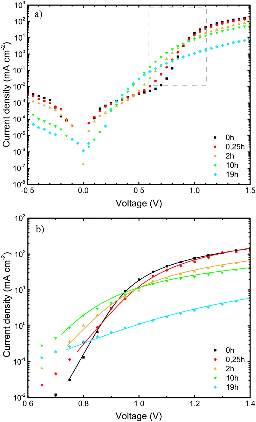 | ||
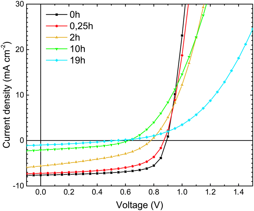
| Fig. 2 (a) Dark J–V characteristics of ITO/MoO3/TQ1:PC70BM/LiF/Al devices, upon exposure of the TQ1:PC70BM active layer to 1 sun (AM1.5) and ambient air for different lengths of time. The gray framed area in (2a) represents a section of the J–V characteristics enlarged in (2b). (b) High voltage region of dark J–V characteristics that was fitted to eqn (2). The lines represent the fitted results. | ||
The ideality factor (n) values, obtained from eqn (1), were introduced into eqn (2), which was used to fit the high forward bias region (see Fig. 4b) in order to extract the series resistance RS. The n and RS values for the different exposure times are listed in Table 1. The value obtained for the ideality factor n for the unexposed sample is 1.24, as seen in Table 1. This is well within the interval 1.2–1.3, which is commonly reported for polymer:fullerene systems42–44 and attributed by Wetzelaer et al.43 to the presence of the fullerene derivatives in the active layer blend. As the exposure progresses, the ideality factor increases to values of about 2 for the 2 h and 10 h exposed samples, indicating that the recombination mechanism has become trap-assisted37 at that point. For the 19 h exposed sample the obtained ideality factor is unrealistically high and the Shockley model fails.
 | ||
| Fig. 3 J–V characteristics measured under AM1.5 illumination of ITO/MoO3/TQ1:PC70BM/LiF/Al solar cells, upon exposure of the TQ1:PC70BM active layer to 1 sun (AM1.5) and ambient air for different lengths of time. | ||
| Exposure time (h) | V OC (V) | J SC (mA cm−2) | FF (%) | PCE (%) |
|---|---|---|---|---|
| 0 | 0.89 ± 0.01 | 7.47 ± 0.28 | 68.3 ± 0.9 | 4.53 ± 0.23 |
| 0.25 | 0.87 ± 0.02 | 7.28 ± 0.69 | 58.2 ± 0.8 | 3.68 ± 0.05 |
| 2 | 0.78 ± 0.01 | 5.21 ± 0.35 | 40.1 ± 1.1 | 1.63 ± 0.09 |
| 10 | 0.63 ± 0.02 | 2.03 ± 0.14 | 39.3 ± 4.9 | 0.50 ± 0.05 |
| 19 | 0.52 ± 0.04 | 0.73 ± 0.21 | 21.9 ± 0.8 | 0.09 ± 0.07 |
3.3 External quantum efficiency (EQE) and UV-vis absorption spectroscopy
In order to investigate which wavelengths of incident light generate charges, the external quantum efficiency (EQE) spectrum was measured. The EQE spectra of the devices were then correlated with the UV-vis absorption spectra of the active layers, with the purpose of determining which stages of light-to-electrical current conversion (photon absorption or charge transport) were affected by the photo-degradation.As shown in Fig. 4, the EQE decreases with increasing exposure time throughout the entire wavelength range 300–700 nm. This result is in agreement with the decrease of JSC with increasing exposure time, as observed in the light J–V characteristics. The decrease is, initially, slightly more pronounced in the 500–700 nm range, where TQ1 is the main absorber. Fig. 5a shows the UV-vis absorption spectrum of TQ1 polymer films, exhibiting two characteristic absorption bands around 350 nm and 620 nm.31,45 The pure TQ1 films photobleach rapidly under simulated sunlight in ambient air, which is seen by the decrease in intensity of both absorption bands.27,46 However, in Fig. 5b, it can be seen that the photobleaching of the TQ1:PC70BM (1:3) blend film in the 500–700 nm range is moderate compared to that of the pure TQ1 film.
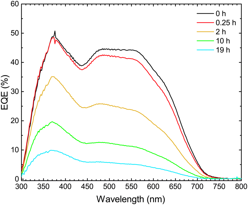 | ||
| Fig. 4 External quantum efficiency spectra of ITO/MoO3/TQ1:PC70BM/LiF/Al solar cells upon exposure of the TQ1:PC70BM active layer to 1 sun (AM1.5) and ambient air for different lengths of time. | ||
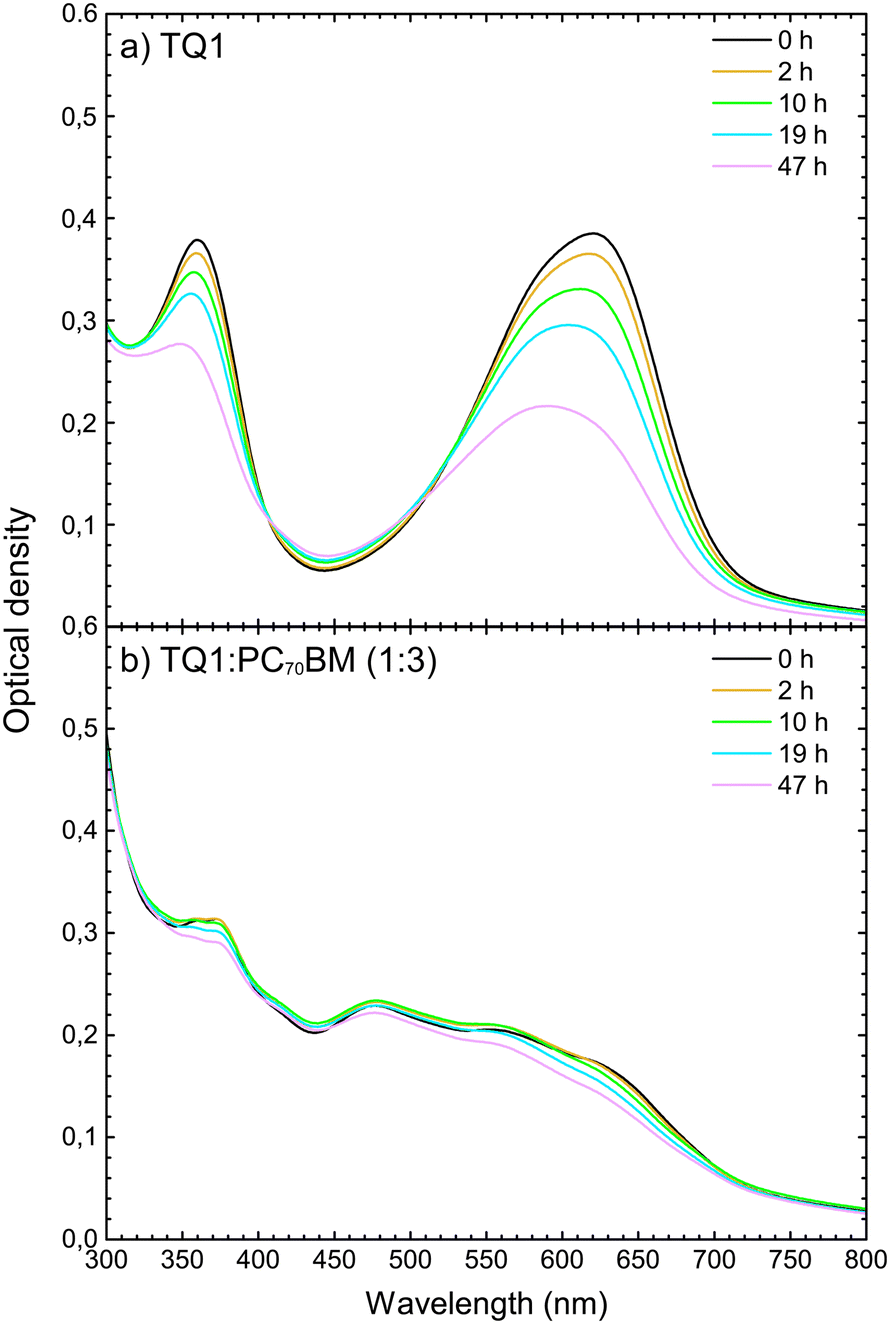 | ||
| Fig. 5 UV-vis absorption spectra of (a) TQ1 films; and (b) TQ1:PC70BM blend films, spin-coated on quartz glass from o-DCB with 2% CN, upon exposure to simulated sunlight and ambient air for different lengths of time. | ||
Comparing the effects of the photo-oxidation of the active layer on the EQE spectra (Fig. 4) and on the absorption spectra (Fig. 5b), we observe that the decrease of EQE of the solar cell is much faster than the decrease in absorption of the active layer. From this comparison it can be deduced that the photobleaching of the active layer is not the major cause of the decrease in short circuit current of the solar cells, observed when the active layer is intentionally exposed to simulated sunlight in ambient air. Therefore, we focus now on the PC70BM component, and investigate whether the electron transport properties and electron collection at the electrodes are affected in this photodegradation process.
3.4 NEXAFS of PC70BM
X-ray absorption resonances in NEXAFS spectra represent transitions from C1s core levels to unoccupied molecular states. As unoccupied molecular states depend on the type of interatomic bonding, these spectra can be used as molecular fingerprints. Hence, they provide insights into chemical changes due to the exposure to light in air. In an attempt to locate the degradation in the film, we investigate here how the surfaces and bulk of pure PC70BM films evolve with exposure time, by using different detection modes of NEXAFS spectroscopy.Fig. 6a–c show C1s NEXAFS spectra of PC70BM, spin coated from chloroform, recorded in PEY, TEY and transmission modes, respectively. The positions of the three peaks (284.3, 285 and 286.1 eV) are similar to those found in the NEXAFS spectra that were published previously.47 The first peak has been assigned to the C1s → π* transitions in the PC70BM molecule and the main contributions are likely to be from the sp2 carbons of the fullerene cage, as is the case for PC60BM.48 The peak intensity, i.e., the probability of transitions, can to some extent be related to the density of available final states for this transition, in other words the density of states (DoS) in the LUMO.
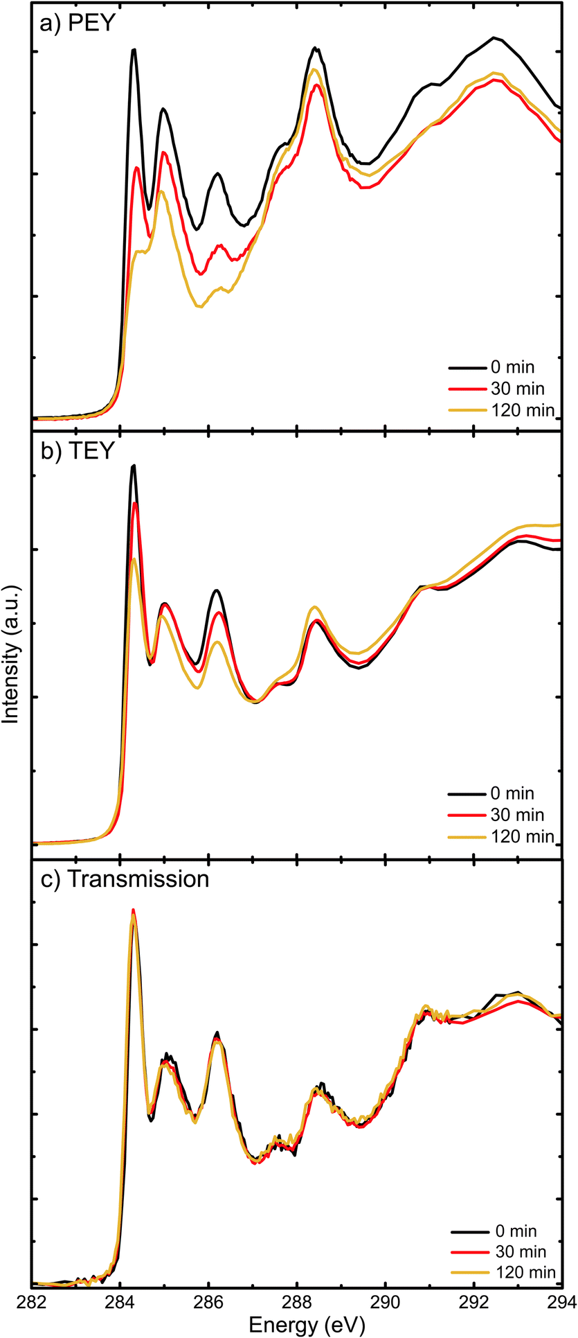 | ||
| Fig. 6 C1s NEXAFS spectra of PC70BM thin films in (a) partial electron yield (PEY) mode; (b) total electron yield (TEY) mode; and (c) transmission mode, upon exposure to simulated sunlight and ambient air for different lengths of time. | ||
As seen in the PEY spectrum (Fig. 6a), the peak at 284.3 eV of the C1s → π* transition from the fullerene cage decreases strongly with increasing exposure time. After 30 minutes of exposure to simulated sunlight and ambient air, the decrease is significant. This is in agreement with the collapse of the C1s → π* peak observed in the PEY-NEXAFS spectra of PC60BM films exposed to light and air.27 In the TEY spectrum (Fig. 6b), the decrease of the peak intensity is not as pronounced. After 2 hours of exposure, the peak is reduced in PEY mode by 55%, but in TEY mode by 25%, with respect to the initial intensities. In transmission mode (Fig. 6c), the changes are negligible. As the PEY and TEY modes have different probing depths, about 3 nm and 10 nm, respectively, the comparison of Fig. 6a and b with the transmission mode (Fig. 6c) shows that the surfaces and near surface regions of the PC70BM films are affected much more rapidly than the bulk by exposure of the films. This indicates that the PC70BM molecules in the film surface lose their conjugated character early in the exposure process (within the first 30 minutes) due to the breaking of the CC bonds of the cage,17,49 which allows the formation of photo-oxidation products. This early carbonyl formation after 15 min exposure is not directly observable in the FT-IR absorption spectrum (Fig. 1b), because the FT-IR measurements are performed in transmission mode and are therefore much less surface sensitive compared to NEXAFS spectroscopy. This would imply that the surfaces of the PC70BM films start to degrade already within 30 min of exposure, as seen from the decrease in the density of unoccupied states by the surface sensitive PEY-NEXAFS, while bulk sensitive transmission NEXAFS cannot detect the presence of significant photodegradation products at all.
3.5 Kelvin probe measurements of PC70BM
As the results obtained from dark J–V measurements indicate the formation of trap states due to the oxidation of PC70BM, pure PC70BM films were investigated further using a Kelvin probe. Work function, SPV and SPS measurements were performed in order to confirm the existence of the traps and determine their nature and their locations in the gap.The work function, measured in the dark in N2, of a freshly spin-coated PC70BM film on a Si substrate is about 4.32 ± 0.01 eV. These PC70BM films do not show any significant surface photovoltage (30 ± 10 mV). After exposure to light in air for 2 hours, the work function of the PC70BM film increases to 4.68 ± 0.01 eV and the SPV signal increases to about 200 mV, both measured using a Kelvin probe in N2. The work function and band bending values are given in Table S1 in the ESI.† The SPV signal is interpreted as due to band flattening under illumination. In the case of photo-oxidized PC70BM films, this is an indication of the presence of an upward band bending. The band bending is induced due to the trap states at the PC70BM surface rather than the PC70BM/substrate interface. This is indicated by the surface photovoltage data and in agreement with the changes observed by surface-sensitive NEXAFS spectroscopy. After longer exposure times, the SPV signal decreases again, reaching 20 mV after 47 hours of exposure (see Fig. S2 in the ESI†), while the work function remains stable (see Fig. S1 in the ESI†).
Fig. 7 shows the surface photovoltage spectrum in the photon energy range 1.1–1.7 eV of a PC70BM film exposed for 2 hours to simulated sunlight in ambient air. From the spectrum the optical gap Eg (position represented by a black, dashed line) was estimated, by plotting the d(CPD)/dE−E diagram and finding the position of the maximum value on the ordinate axis (not shown).39 The obtained value for the optical gap Eg is 1.72 eV, which is similar to values that have been reported previously for the parent molecule C70.50,51
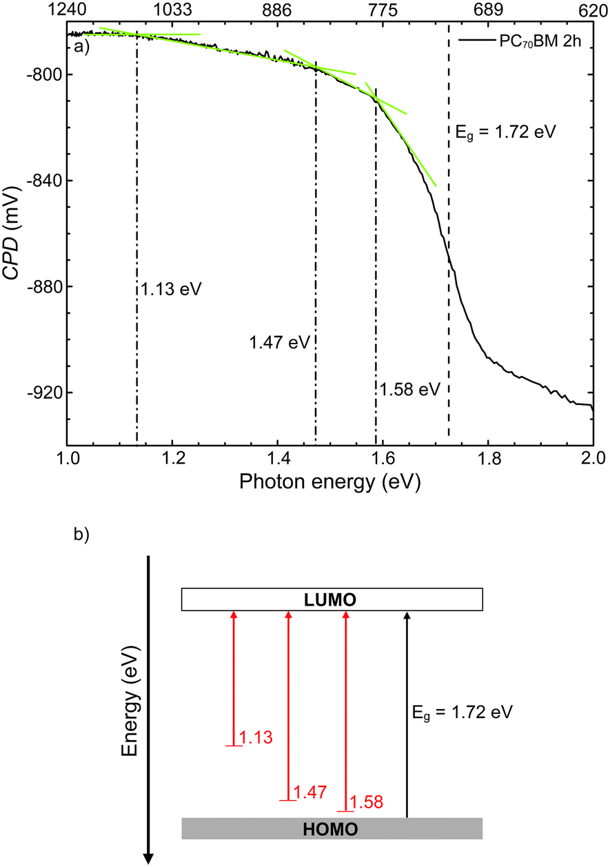 | ||
| Fig. 7 (a) Surface photovoltage spectrum of a PC70BM thin film on a silicon substrate after 2 h exposure to simulated sunlight in ambient air. The black, dashed line indicates the optical gap Eg = 1.72 eV, determined by the global maximum position in d(CPD)/dE − E. The dashed-dotted lines represent the estimated positions of the transitions from filled gap states to the LUMO, at 1.58 eV, 1.47 eV and 1.13 eV, respectively, resulting from the changes in slope of the SPS spectrum. (b) Energy band diagram of the PC70BM film, based on the extracted values for the band gap and transitions from gap states to the LUMO band from the SPS spectrum (a). | ||
From the changes in slope in the SPV spectrum, or by plotting the d2(CPD)/dE2−E diagram, one can estimate the energy positions and the nature of gap states. Three gap states can be identified at the surface of PC70BM exposed for 2 hours, at 1.58 eV, 1.47 eV and 1.13 eV from the HOMO. Their positions with respect to one of the bands are found by determining the crossing points of the tangents to the linear parts of the sub-bandgap part of the SPS spectrum, as indicated in Fig. 7. In the case where the slope decreases (i.e., d2(CPD)/dE2 < 0), these positions correspond with transitions from the filled gap state (near the HOMO) to the LUMO band and, vice versa, if the slope increases (i.e., d2(CPD)/dE2 > 0), the positions correspond to transitions from the HOMO to empty gap states near the LUMO (Fig. 7).39,52,53 Therefore, on 2 hour exposed PC70BM, the observed states near the HOMO (filled states) donate electrons to the LUMO upon illumination, hence flattening the band (donor type). Given that the blend film and PC70BM film undergo similar degradation, as shown by FT-IR results, these gap states in the photodegraded PC70BM films may also be present on the surface of the TQ1:PC70BM blend active layer, and hence act as traps in the solar cell.
4. Discussion
In this work we set out to investigate the causes of the electrical performance degradation in a polymer–fullerene solar cell when its photoactive layer, consisting of the TQ1:PC70BM (1:3) blend, is intentionally exposed to light and air. By a set of spectroscopy techniques we studied the effects of such exposure on the material properties of the donor:acceptor blend and its individual components, and correlate that with the performance of the corresponding solar cell, for increasing exposure times.
We have found that upon intentional exposure to light and air: (1) the absorption of the TQ1:PC70BM blend film decreases (almost) linearly by roughly 18% within 47 h exposure time over the 500–700 nm spectral range, but at a considerably lower rate than that of the pristine TQ1 film; (2) PC70BM molecules lose their conjugation, which indicates that the density of states in the LUMO in PC70BM decreases; (3) this loss of conjugation of PC70BM occurs mainly at the surfaces and in the sub-surface regions (10 nm) of the PC70BM films, while the PC70BM in the bulk remains mainly undisturbed for shorter exposure times; (4) carbonyls are formed in films of TQ1, on the fullerene cage of PC70BM, and in the blend films after exposure times of 2 hours and longer; and (5) filled gap states are found near the HOMO in the PC70BM films exposed for 2 hours, and an upward band bending develops as a consequence of charge redistribution at the surface.
From the electrical characterisation of the OSC devices based on these photoactive layers, exposed for different duration times and completed by a fresh LiF/Al cathode, we found that: (1) the forward-bias current (in the dark) and the short circuit current (under illumination) decrease with increasing exposure time due to the increase of the series resistance RS; (2) the diode ideality factor, n, increases from 1.2 to 2; (3) the built-in potential does not change up to 10 hours of exposure, but changes drastically after 19 hours; and (4) the EQE decreases over the whole spectral range with exposure time, with a significantly faster rate than the decrease in absorption.
The increased series resistance is in line with the loss of conjugation in PC70BM molecules and the consequent less efficient electron transport through degraded PC70BM, in the dark as well as under illumination. While demonstrated here by NEXAFS for pure PC70BM films, this loss of conjugation in PC70BM also occurs in blend films where PC70BM is surrounded with TQ1. Breaking of CC bonds allows the attachment of the oxygen from ambient air, leading to the formation of carbonyl (CO) in the TQ1 and PC70BM pristine films as well as in the blend thin films, as seen from FT-IR spectra. The comparable amounts of carbonyl growth observed in the FT-IR spectra of the PC70BM and TQ1:PC70BM blend films strengthen this argument and indicate that the presence of TQ1 does not hinder the photo-oxidation of PC70BM in the blend.
The increased ideality factor is consistent with the existence of charge traps and development of the trap-assisted recombination. The presence of traps was deduced from the observation of upward band bending developing during the first 2 hours of exposure of the neat PC70BM films. These shallow states may serve as electron traps in PC70BM. Both the ideality factor and the band bending start to increase significantly already after 15 minutes of exposure, and become fully developed after 2 hours of exposure. The early photo-oxidation of PC70BM and the formation of shallow traps near the HOMO may also account for the decrease of the fill factor. For the 2 h exposure time the locations of the most significant gap states in the neat PC70BM films were found to be filled donor-type states close to the HOMO. These shallow states in PC70BM may serve as electron traps.
The drastic change in the built-in potential after 19 hours of exposure indicates that other additional processes are activated for longer exposure times. This change in dark and light characteristics is in line with the decrease of the SPV signal (band bending) observed for the 19 and 47 h exposed PC70BM films, which is likely to be an indication for a wider distribution of gap states of different types (filled and unfilled) throughout the bandgap. Since this occurs without any significant change in the work function, it must mean that the LUMO (electron affinity) of the PC70BM has changed after these long exposure times. That is likely to contribute significantly to the loss of VOC and the built-in potential in these cases. In addition, the degradation of the density of states of the HOMO of TQ1 after long exposure times, reported earlier (see Hansson et al.27), may also contribute to this loss in voltage.
Since the decrease in EQE of the solar cells is stronger than the decrease in absorption of the corresponding degraded active layer, we conclude that the loss in light absorption is not the major contributor to the decreasing performance of TQ1:PC70BM organic solar cells. It is rather the deficient charge transport and the increased trap-assisted recombination that are responsible for the device degradation.
The mechanism for the loss of conjugation due to the breaking of CC bonds in the PC70BM cage is similar to what has been previously established for PC60BM, both theoretically by Brumboiu et al.48,54 and experimentally by Anselmo et al.25 The breaking of CC bonds may also lead to the opening of the C70 cage.17 In contrast to the TQ1:PC60BM blend (Hansson et al.27), the presence of TQ1 decelerates the photo-oxidation of the PC70BM component in the TQ1:PC70BM blend. Given the slightly lower rate of photo-oxidation for PC70BM as compared to PC60BM,26 this then implies that the TQ1:PC70BM blend must be more stable against photo-oxidation than the TQ1:PC60BM blend.
The formation of trap states near the HOMO, as observed here for photo-oxidized PC70BM thin films, has also been predicted for PC60BM through DFT calculations by Lee et al.24 They showed that the photo-oxidation products of PC60BM, including epoxides, diols and carbonyls, shift the positions of the LUMO and the HOMO by different amounts, due to the formation of trap states near the LUMO and the HOMO. Our SPS spectrum for the 2 hour exposed PC70BM film does not show any evidence for the presence of gap states near the LUMO. However, this does not exclude the possibility that after longer exposure times other types of trap states may form near the LUMO, as a consequence of the development of more complex oxidation products. An indication of that is our observation that the intensity of the SPV signal decreases from 200 mV (after 2 h exposure) to 20 mV (after 47 h exposure), as shown in Fig. S2 in the ESI.† This decrease in the band bending may indicate the development of a wider distribution of gap states, both of acceptor and donor types. A similar effect was shown for C60 by Mishori et al.38 An increased exposure time could then lead to a decrease of the fullerene's LUMO, as suggested for PC60BM from time-dependent DFT calculations by Reese et al.23
5. Conclusions
In this work, we have studied the effect that the exposure of TQ1:PC70BM active layers (prior to cathode deposition) to simulated sunlight and ambient air has on the performance of solar cells with the conventional structure (ITO/MoO3/TQ1:PC70BM/LiF/Al) and have correlated the electrical degradation with the photo-oxidation of the active layer materials. Electrical characterisation results (dark and light J–V, EQE) compared with UV-vis spectra indicate that the major contribution to the performance degradation comes from a decline of the charge transport and collection, rather than from the decreased absorption. The transport and collection of charge carriers are affected by the formation of traps at the surface of the active layer. In pristine PC70BM films exposed for 2 hours, the presence of trap states near the HOMO and the consequent upward band bending at the surface are demonstrated. We propose here that the origin of these trap states is the photo-oxidation products of PC70BM, which have a significant carbonyl signature observed in FT-IR spectra. Moreover, FT-IR spectroscopy also shows that even TQ1 photo-oxidizes. This study demonstrates that the photo-oxidation of fullerenes is the main cause of performance loss in OPV devices when exposed to air. Replacing fullerenes as electron acceptor materials with more stable non-fullerene acceptors may, apart from their improved power conversion efficiencies, also be beneficial for extending the device lifetime.Conflicts of interest
There are no conflicts of interest to declare.Acknowledgements
The authors thank Sebastian Ekhagen at Karlstad University for complementary Kelvin Probe experiments. The authors are grateful to Dr Ben Watts for technical advice and assistance at the beamline PolLux (X07DA) of the Swiss Light Source, at the Paul Scherrer Institute, Villigen, Switzerland. Beamline staff at beamline D1011 at MAX IV is acknowledged for technical assistance during the NEXAFS measurements. E. M. acknowledges the COST Action MP1307 StableNextSol for STSM support to the Weizmann Institute of Science in Israel. E. M. acknowledges financial support for this research from the Swedish Energy Council, contract number 38327-1, the Swedish Research Council, grant 2015-03778, and the Knut and Alice Wallenberg Foundation, contract 2016.0059.References
- R. Søndergaard, M. Hösel, D. Angmo, T. T. Larsen-Olsen and F. C. Krebs, Roll-to-roll fabrication of polymer solar cells, Mater. Today, 2012, 15, 36–49 CrossRef.
- J. Huang, X. Zhang, D. Zheng, K. Yan, C.-Z. Li and J. Yu, Boosting Organic Photovoltaic Performance Over 11% Efficiency With Photoconductive Fullerene Interfacial Modifier, Sol. RRL, 2017, 1, 1600008 CrossRef.
- K. Feng, J. Yuan, Z. Bi, W. Ma, X. Xu, G. Zhang and Q. Peng, Low-Energy-Loss Polymer Solar Cells with 14.52% Efficiency Enabled by Wide-Band-Gap Copolymers, Science, 2019, 12, 1–12 CAS.
- G. Liu, J. Jia, K. Zhang, X. Jia, Q. Yin, W. Zhong, L. Li, F. Huang and Y. Cao, 15% Efficiency Tandem Organic Solar Cell Based on a Novel Highly Efficient Wide-Bandgap Nonfullerene Acceptor with Low Energy Loss, Adv. Energy Mater., 2019, 9, 1803657 CrossRef.
- Z. Bi, Q. Zhu, X. Xu, H. B. Naveed, X. Sui, J. Xin, L. Zhang, T. Li, K. Zhou, X. Liu, X. Zhan and W. Ma, Efficient Quaternary Organic Solar Cells with Parallel-Alloy Morphology, Adv. Funct. Mater., 2019, 29, 1806804 CrossRef.
- V. I. Madogni, B. Kounouhéwa, A. Akpo, M. Agbomahéna, S. A. Hounkpatin and C. N. Awanou, Comparison of degradation mechanisms in organic photovoltaic devices upon exposure to a temperate and a subequatorial climate, Chem. Phys. Lett., 2015, 640, 201–214 CrossRef CAS.
- S. Rafique, S. M. Abdullah, K. Sulaiman and M. Iwamoto, Fundamentals of bulk heterojunction organic solar cells: an overview of stability/degradation issues and strategies for improvement, Renewable Sustainable Energy Rev., 2018, 84, 43–53 CrossRef.
- M. Jørgensen, K. Norrman and F. C. Krebs, Stability/degradation of polymer solar cells, Sol. Energy Mater. Sol. Cells, 2008, 92, 686–714 CrossRef.
- E. Voroshazi, B. Verreet, A. Buri, R. Müller, D. Di Nuzzo and P. Heremans, Influence of cathode oxidation via the hole extraction layer in polymer:fullerene solar cells, Org. Electron., 2011, 12, 736–744 CrossRef CAS.
- M. Bag, S. Banerjee, R. Faust and D. Venkataraman, Self-healing polymer sealant for encapsulating flexible solar cells, Sol. Energy Mater. Sol. Cells, 2016, 145, 418–422 CrossRef CAS.
- W. R. Mateker and M. D. McGehee, Progress in Understanding Degradation Mechanisms and Improving Stability in Organic Photovoltaics, Adv. Mater., 2017, 29, 1603940 CrossRef PubMed.
- X. Guo, N. Zhou, S. J. Lou, J. Smith, D. B. Tice, J. W. Hennek, R. P. Ortiz, J. T. L. Navarrete, S. Li, J. Strzalka, L. X. Chen, R. P. H. Chang, A. Facchetti and T. J. Marks, Polymer solar cells with enhanced fill factors, Nat. Photonics, 2013, 7, 825–833 CrossRef CAS.
- V. Shrotriya, G. Li, Y. Yao, C.-W. Chu and Y. Yang, Transition metal oxides as the buffer layer for polymer photovoltaic cells, Appl. Phys. Lett., 2006, 88, 073508 CrossRef.
- E. Andreoli, K.-S. Liao, A. Haldar, N. J. Alley and S. A. Curran, PPy:PSS as alternative to PEDOT:PSS in organic photovoltaics, Synth. Met., 2013, 185–186, 71–78 CrossRef CAS.
- M. Manceau, E. Bundgaard, J. E. Carlé, O. Hagemann, M. Helgesen, R. Søndergaard, M. Jørgensen and F. C. Krebs, Photochemical stability of π-conjugated polymers for polymer solar cells: a rule of thumb, J. Mater. Chem., 2011, 21, 4132 RSC.
- M. Wohlers, H. Werner, D. Herein, T. Schedel-Niedrig, A. Bauer and R. Schlögl, Reaction of C60 and C70 with molecular oxygen, Synth. Met., 1996, 77, 299–302 CrossRef CAS.
- M. Wohlers, H. Werner, T. Belz, T. Rühle and R. Schlögl, C60: a host lattice for the intercalation of oxygen?, Mikrochim. Acta, 1997, 125, 401–406 CrossRef CAS.
- M. Wohlers, A. Bauer, T. Rühle, F. Neitzel, H. Werner and R. Schlögl, The Dark Reaction of C 60 and of C 70 with Molecular Oxygen at Atmospheric Pressure and Temperatures between 300 K and 800 K, Fullerene Sci. Technol., 1997, 5, 49–83 CrossRef CAS.
- S. Chambon, A. Rivaton, J.-L. Gardette and M. Firon, Photo- and thermal degradation of MDMO-PPV:PCBM blends, Sol. Energy Mater. Sol. Cells, 2007, 91, 394–398 CrossRef CAS.
- P. C. Eklund, A. M. Rao, P. Zhou, Y. Wang, K.-A. Wang, G. T. Hager and J. M. Holden, Optical studies of fullerene-based solids, Mater. Sci. Eng., B, 1993, 19, 154–161 CrossRef.
- R. A. Assink, J. E. Schirber, D. A. Loy, B. Morosin and G. A. Carlson, Intercalation of molecular species into the interstitial sites of fullerene, J. Mater. Res., 1992, 7, 2136–2143 CrossRef CAS.
- C. C. Eloi, D. J. Robertson, A. M. Rao, P. Zhou, K.-A. Wang and P. C. Eklund, An investigation of photoassisted diffusion of oxygen in solid C60 films using resonant alpha-scattering, J. Mater. Res., 1993, 8, 3085–3089 CrossRef CAS.
- M. O. Reese, A. M. Nardes, B. L. Rupert, R. E. Larsen, D. C. Olson, M. T. Lloyd, S. E. Shaheen, D. S. Ginley, G. Rumbles and N. Kopidakis, Photoinduced Degradation of Polymer and Polymer–Fullerene Active Layers: Experiment and Theory, Adv. Funct. Mater., 2010, 20, 3476–3483 CrossRef CAS.
- H. K. H. Lee, A. M. Telford, J. A. Röhr, M. F. Wyatt, B. Rice, J. Wu, A. de Castro Maciel, S. M. Tuladhar, E. Speller, J. McGettrick, J. R. Searle, S. Pont, T. Watson, T. Kirchartz, J. R. Durrant, W. C. Tsoi, J. Nelson and Z. Li, The role of fullerenes in the environmental stability of polymer:fullerene solar cells, Energy Environ. Sci., 2018, 11, 417–428 RSC.
- A. S. Anselmo, A. Dzwilewski, K. Svensson and E. Moons, Photodegradation of the electronic structure of PCBM and C60 films in air, Chem. Phys. Lett., 2016, 652, 220–224 CrossRef CAS.
- V. Blazinic, L. K. E. Ericsson, S. A. Muntean and E. Moons, Photo-degradation in air of spin-coated PC60BM and PC70BM films, Synth. Met., 2018, 241, 26–30 CrossRef CAS.
- R. Hansson, C. Lindqvist, L. K. E. Ericsson, A. Opitz, E. Wang and E. Moons, Photo-degradation in air of the active layer components in a thiophene–quinoxaline copolymer:fullerene solar cell, Phys. Chem. Chem. Phys., 2016, 18, 11132–11138 RSC.
- E. M. Speller, J. D. McGettrick, B. Rice, A. M. Telford, H. K. H. Lee, C.-H. Tan, C. S. De Castro, M. L. Davies, T. M. Watson, J. Nelson, J. R. Durrant, Z. Li and W. C. Tsoi, Impact of Aggregation on the Photochemistry of Fullerene Films: Correlating Stability to Triplet Exciton Kinetics, ACS Appl. Mater. Interfaces, 2017, 9, 22739–22747 CrossRef CAS PubMed.
- Y. Matsuo, A. Ozu, N. Obata, N. Fukuda, H. Tanaka and E. Nakamura, Deterioration of bulk heterojunction organic photovoltaic devices by a minute amount of oxidized fullerene, Chem. Commun., 2012, 48, 3878 RSC.
- N. Y. Doumon, F. V. Houard, J. Dong, P. Christodoulis, M. V. Dryzhov, G. Portale and L. J. A. Koster, Improved photostability in ternary blend organic solar cells: the role of [70]PCBM, J. Mater. Chem. C, 2019, 7, 5104–5111 RSC.
- E. Wang, L. Hou, Z. Wang, S. Hellström, F. Zhang, O. Inganäs and M. R. Andersson, An Easily Synthesized Blue Polymer for High-Performance Polymer Solar Cells, Adv. Mater., 2010, 22, 5240–5244 CrossRef CAS PubMed.
- W. Kern, The Evolution of Silicon Wafer Cleaning Technology, J. Electrochem. Soc., 1990, 137, 1887 CrossRef CAS.
- B. Watts, L. Thomsen and P. C. Dastoor, Methods in carbon K-edge NEXAFS: experiment and analysis, J. Electron Spectrosc. Relat. Phenom., 2006, 151, 105–120 CrossRef CAS.
- B. Watts and H. Ade, A simple method for determining linear polarization and energy calibration of focused soft X-ray beams, J. Electron Spectrosc. Relat. Phenom., 2008, 162, 49–55 CrossRef CAS.
- W. N. Hansen and G. J. Hansen, Standard reference surfaces for work function measurements in air, Surf. Sci., 2001, 481, 172–184 CrossRef CAS.
- T. Kirchartz, F. Deledalle, P. S. Tuladhar, J. R. Durrant and J. Nelson, On the Differences between Dark and Light Ideality Factor in Polymer:Fullerene Solar Cells, J. Phys. Chem. Lett., 2013, 4, 2371–2376 CrossRef CAS.
- G.-J. A. H. Wetzelaer and P. W. M. Blom, Diffusion-driven currents in organic-semiconductor diodes, NPG Asia Mater., 2014, 6, e110–e110 CrossRef CAS.
- B. Mishori, E. A. Katz, D. Faiman and Y. Shapira, Studies of electron structure of C60 thin films by surface photovoltage spectroscopy, Solid State Commun., 1997, 102, 489–492 CrossRef CAS.
- L. Kronik, Surface photovoltage phenomena: theory, experiment, and applications, Surf. Sci. Rep., 1999, 37, 1–206 CrossRef CAS.
- Y. Wang, M. J. Jafari, N. Wang, D. Qian, F. Zhang, T. Ederth, E. Moons, J. Wang, O. Inganäs, W. Huang and F. Gao, Light-induced degradation of fullerenes in organic solar cells: a case study on TQ1:PC71BM, J. Mater. Chem. A, 2018, 6, 11884–11889 RSC.
- U. Dettinger, H.-J. Egelhaaf, C. J. Brabec, F. Latteyer, H. Peisert and T. Chassé, FTIR Study of the Impact of PC[60]BM on the Photodegradation of the Low Band Gap Polymer PCPDTBT under O2 Environment, Chem. Mater., 2015, 27, 2299–2308 CrossRef CAS.
- L. J. A. Koster, V. D. Mihailetchi, R. Ramaker and P. W. M. Blom, Light intensity dependence of open-circuit voltage of polymer:fullerene solar cells, Appl. Phys. Lett., 2005, 86, 123509 CrossRef.
- G. A. H. Wetzelaer, M. Kuik, M. Lenes and P. W. M. Blom, Origin of the dark-current ideality factor in polymer:fullerene bulk heterojunction solar cells, Appl. Phys. Lett., 2011, 99, 153506 CrossRef.
- K. Tvingstedt and C. Deibel, Temperature Dependence of Ideality Factors in Organic Solar Cells and the Relation to Radiative Efficiency, Adv. Energy Mater., 2016, 6, 1502230 CrossRef.
- R. Singh, G. Pagona, V. G. Gregoriou, N. Tagmatarchis, D. Toliopoulos, Y. Han, Z. Fei, A. Katsouras, A. Avgeropoulos, T. D. Anthopoulos, M. Heeney, P. E. Keivanidis and C. L. Chochos, The impact of thienothiophene isomeric structures on the optoelectronic properties and photovoltaic performance in quinoxaline based donor–acceptor copolymers, Polym. Chem., 2015, 6, 3098–3109 RSC.
- P. Henriksson, C. Lindqvist, B. Abdisa, E. Wang, Z. George, R. Kroon, C. Müller, T. Yohannes, O. Inganäs and M. R. Andersson, Stability study of quinoxaline and pyrido pyrazine based co-polymers for solar cell applications, Sol. Energy Mater. Sol. Cells, 2014, 130, 138–143 CrossRef CAS.
- B. Watts, S. Swaraj, D. Nordlund, J. Lüning and H. Ade, Calibrated NEXAFS spectra of common conjugated polymers, J. Chem. Phys., 2011, 134, 024702 CrossRef CAS PubMed.
- I. E. Brumboiu, L. Ericsson, R. Hansson, E. Moons, O. Eriksson and B. Brena, The influence of oxygen adsorption on the NEXAFS and core-level XPS spectra of the C60 derivative PCBM, J. Chem. Phys., 2015, 142, 054306 CrossRef PubMed.
- M. Wohlers, A. Bauer, T. Belz, T. Rühle, T. Schedel-Niedrig, R. Schlögl, H. Werner and A. Bauer, The mechanism of oxidation of fullerenes with molecular oxygen, ACS Div. Fuel Chem. Prepr., 1996, 41, 108–112 CAS.
- W. Zhou, S. Xie, S. Qian, T. Zhou, R. Zhao, G. Wang, L. Qian and W. Li, Optical absorption spectra of C70 thin films, J. Appl. Phys., 1996, 80, 459–463 CrossRef CAS.
- H. Habuchi, S. Nitta, D. Han and S. Nonomura, Localized electronic states related to O2 intercalation and photoirradiation on C60 films and C70 films, J. Appl. Phys., 2000, 87, 8580–8588 CrossRef CAS.
- E. Fefer, Y. Shapira and I. Balberg, Direct determination of the band-gap states in hydrogenated amorphous silicon using surface photovoltage spectroscopy, Appl. Phys. Lett., 1995, 67, 371–373 CrossRef CAS.
- B. Mishori, Y. Shapira, A. Belu-Marian, M. Manciu and A. Devenyi, Studies of C60 thin films using surface photovoltage spectroscopy, Chem. Phys. Lett., 1997, 264, 163–167 CrossRef CAS.
- I. E. Brumboiu, A. S. Anselmo, B. Brena, A. Dzwilewski, K. Svensson and E. Moons, Near-edge X-ray absorption fine structure study of the C60-derivative PCBM, Chem. Phys. Lett., 2013, 568–569, 130–134 CrossRef.
Footnote |
| † Electronic supplementary information (ESI) available. See DOI: 10.1039/c9cp04384e |
| This journal is © the Owner Societies 2019 |