
 Open Access Article
 This Open Access Article is licensed under a Creative Commons Attribution-Non Commercial 3.0 Unported Licence
Refractive index change dominates the transient absorption response of metal halide perovskite thin films in the near infrared†
Hannu P.
Pasanen
 *a,
Paola
Vivo
a,
Laura
Canil
b,
Antonio
Abate
b and
Nikolai
Tkachenko
*a
*a,
Paola
Vivo
a,
Laura
Canil
b,
Antonio
Abate
b and
Nikolai
Tkachenko
*a
aChemistry and Advanced Materials Group, Faculty of Engineering and Natural Sciences, Tampere University, Korkeakoulunkatu 8, FI-33720 Tampere, Finland. E-mail: hannu.pasanen@tuni.fi; nikolai.tkachenko@tuni.fi; Tel: +358 408746170
bHelmholtz-Zentrum Berlin für Materialien und Energie, Kekuléstraße 5, 12489 Berlin, Germany
First published on 6th June 2019
Abstract
Perovskites have lately attracted a lot of attention as promising materials for the next-generation of efficient, low-cost, and solution processable optoelectronics. Their complex transient photophysics, in time scales ranging from femtoseconds to seconds, have been widely investigated. However, in most of the reported works the spectral window of ultrafast transient absorption (TA) spectroscopy of perovskite films is limited to the visible region, hence missing crucial information coming from the near-infrared (NIR). Furthermore, the measured TA responses are affected by light interference in a thin perovskite layer making data interpretation a challenge even in the visible part of the spectrum. Here, we demonstrate a method that allows us to separately obtain the changes in absorption and refractive index from conventional transmission and reflection pump–probe measurements. We show that the contribution of the absorption change to the response of metal halide perovskite thin films in the NIR is much smaller than that of the refractive index change. Furthermore, the spectral shape of TA responses in the NIR range is predominantly determined by perovskite layer thickness and its refractive index. However, the time profile of the responses bears important information on the carrier dynamics and makes the NIR a useful range to study perovskite photophysics.
1 Introduction
Recently, metal halide perovskites have gained extensive interest as wonder materials for photovoltaics due to the skyrocketing enhancements in the power conversion efficiencies, up to 24.2%, in just less than a decade.1–3 In addition, perovskites have proven to be promising semiconductors for other applications as well, and particularly for light-emitting diodes,4,5 lasers,6 and photodetectors.7,8 The remarkable performance of perovskite materials in different optoelectronics applications is attributed to their high absorption coefficient, low charge carrier recombination, low exciton binding energy, high charge-carrier mobility, long charge diffusion length for both electrons and holes, and tunable bandgap in the visible range.9The photophysical properties of perovskite complexes have been extensively investigated by steady-state and time-resolved absorption and photoluminescence spectroscopy in a broad time domain ranging from femtoseconds to seconds.10–13 Ultrafast transient absorption (TA) provides key information on the excited state dynamics in perovskites, and particularly on the free carrier dynamics, charge recombination, effective mass, and bandgap renormalization.14–17 However, in most of the reported works the spectral window of TA spectroscopy of perovskite films is limited to the visible region, thus precluding crucial information coming from the near-infrared (NIR).18 On the other hand, TA measurements in the NIR are easy to conduct because relatively thick samples can be utilized. A reason for the scarce investigation in the NIR region can be an unusual spectral pattern that makes the data interpretation challenging. Indeed, in both the visible and NIR range, the transmission spectral shape is affected by the overlapping of simultaneous changes in the absorption coefficient (Δα) and in the refractive index (Δn) because the change in the refractive index manifests itself as the change in reflectance. Lately, several methods to quantify the photoinduced refractive index changes in metal halide perovskite films have been proposed.14,19–22 Nevertheless, the approaches proposed so far are either very difficult to implement experimentally or have led to different interpretations of the importance and scale of the phenomena.21 Tamming et al. have modified a standard TA setup with a white light pulse interferometer to probe the refractive index changes on ultrafast time scales,14 but these modifications severely limited the timescale and require further updates, making it a difficult approach from a practical perspective. Other groups have used Kramers–Kronig (KK) relations to calculate Δn,19,22 but in order to use KK the change in the absorbance coefficient must already be known or approximated in some way. Hence for accurate results the two values, Δn and Δα, must be solved simultaneously.
Here, we demonstrate a method to obtain the changes in absorption and in the refractive index from standard transmission and reflectance pump–probe measurements of thin metal halide perovskite films with homogeneous coverage. The method can be applied to study photo-dynamics of any homogeneous layer with uniform charge carrier distribution and thickness from sub- to few microns, and is particularly useful for measurements in the wavelength ranges outside of the layer absorption bands. In the case of perovskite these are the wavelengths on the red side of the band gap, typically >800 nm. We found that for a roughly 500 nm thick perovskite layer the TA response in the NIR is dominated by the refractive index change, which can be interpreted as the change of the medium polarizability and thus reflects the carrier dynamics. However, this also means that great care needs to be taken not to mischaracterize TA peaks generated by refractive index change when using NIR to study phenomena such as polarons23 or charge transfers from the metal halide perovskite layer to other layers.24
2 Theory and data analysis
We want to account for the active film thickness which is compatible with the monitoring light wavelength and results in an interference pattern in the transmission and reflectance spectra of the sample. For this purpose we will use a simplified sample presentation assuming that our perovskite thin layer has uniform thickness and it is deposited on a thick transparent substrate such as a glass plate. The light propagation through such a sample is schematically presented in Fig. 1.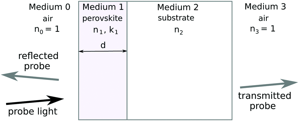 | ||
| Fig. 1 The sample structure and important parameters (refractive indexes) accounted for by the model. | ||
When the thickness of the photo-active layer (metal halide perovskite layer in our case) is comparable with the wavelength, the interference of the waves reflected from the air–layer and layer–glass interfaces affects the spectra of transmitted and reflected light. We will use a theory/model developed by Barybin and Shapovalov,25 and adapt it to the case of the transient absorption measurements of a photo-active medium which is transparent or slightly absorbing in the wavelength range of interest. In application to the model presented in ref. 25 this means:
Medium 0 is air on one side of the layer of interest, it has refractive index n0 = 1 (air), and monitoring (and excitation) light propagates through the sample from this side;
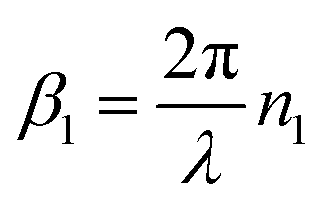
Medium 1 is the photo-active layer of interest (metal halide perovskite film in our case) that has complex refractive index ñ1 = n1 + ik1, where the absorption coefficient is α1 = 2πk1/λ. It is a slightly absorbing medium, meaning n12 ≫ k12; this layer is responsible for the interference pattern and its photo-excitation leads to a (small) change of both the real, Δn1, and imaginary, Δk1, parts of the refractive index, thus contributing to the transient absorption response of the sample;
Medium 2 is the substrate, it is thick (thickness ≫ λ) meaning that it does not contribute to the interference pattern, and it is a transparent medium ñ2 = n2 + ik2 = n2 (or k2 = 0);
Medium 3 is “air” after the sample, or n3 = 1.
In addition, we will consider only the case of normal light incidence. Measurements were done with a small angle of incidence (≈8°) in both reflectance and transmittance modes, which produces negligible difference.
The reflectance (R) and transmittance (T) coefficients were derived in ref. 25 (eqn (60) and (61)) and will be used here:
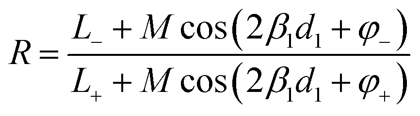 | (1) |
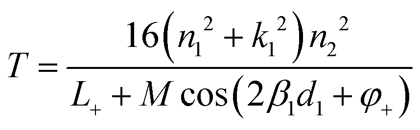 | (2) |
 . The expressions for L± and M can be found in ESI.†
The pump–probe experiments are carried out with low excitation density; therefore we can limit our consideration to small changes of the real part of the refractive index n1(t) = n1 + Δn1(t) and the imaginary part k1(t) = k1 + Δk1(t). Thus we can expect only a small change in transmittance and reflectance, and use the linear approximation
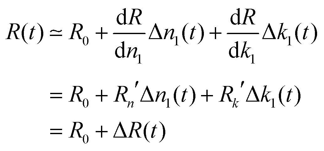 | (3) |
 | (4) |
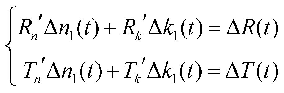 | (5) |
The solutions for Δn1 and Δk1 are
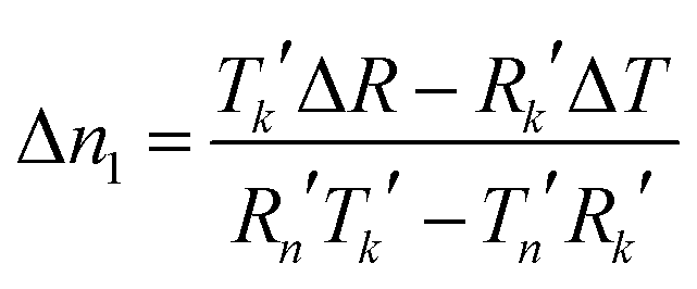 | (6) |
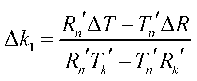 | (7) |
Next we need to find connections between “standard” pump–probe measurements and ΔR and ΔT. The typical output of pump–probe measurements is the photo-induced change of optical density
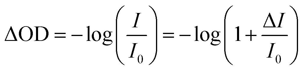 | (8) |
Standard pump–probe measurements are transmittance mode measurements, and the monitoring intensity changes as 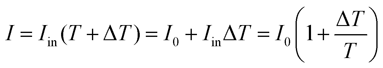 . Therefore, the relation between ΔOD and ΔT is
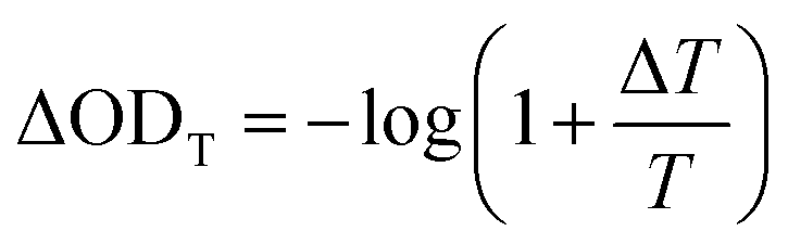 | (9) |
If the detection is switched to measure probe light reflected from the sample surface, the intensities I0 and I are intensities of the reflected light without and with excitation, and the measured value is
 | (10) |
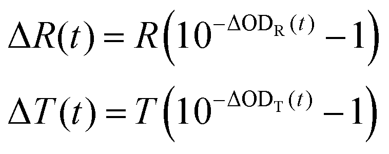 | (11) |
In conclusion, the measurements and data analysis will be carried out following the steps:
1. measure steady state absorption spectra and do initial estimation of the sample thickness by fitting the transmission spectrum provided by eqn (2) to the measured one,
2. carry out pump–probe measurements in transmittance (ΔODT) and reflectance (ΔODR) modes in otherwise identical conditions,
3. do necessary group velocity compensation to align in time the measured spectra, and
4. use eqn (6) and (7) to calculate Δn1 and Δk1 at the delay time and wavelength of interest or to obtain complete wavelength–delay time dependence, Δn1(t,λ) and Δk1(t,λ).
In the last step attention needs to be paid to the determinant of system (5), Rn′Tk′–Tn′Rk′, since it may approach zero as will be discussed later.
3 Results and discussion
The measurements have been performed on metal halide perovskite layers deposited on soda-lime glass through spin coating, following the procedure described by Saliba et al. for high efficiency perovskite solar cells.26 The composition is FAMACs-perovskite, i.e. the so called “triple cation perovskite”, which is well known for giving solar cells with good stability and efficiencies exceeding 20%.26–283.1 Steady state absorption and reflectance spectra
The measured spectrum of a sample prepared for transient absorption studies is shown in Fig. 2. It has strong absorption in the visible part, a sharp drop of the absorption at the wavelength corresponding to the band gap, around 780 nm, and a wavy shape absorption in the near infrared part of the spectrum. The real absorption in the NIR is negligibly small as the perceived absorption is almost entirely caused by reflectance and this wavy shape is due to the interference of light reflected from both sides of the thin perovskite layer. To model sample transmittance T and reflectance R, the perovskite spectra n1(λ) and k1(λ) reported by Phillips et al.29 were used. The k1(λ) spectrum is presented in Fig. 2. The glass substrate n2(λ) spectrum was modelled using the Sellmeier equation with coefficients provided for BK7 glass (see ESI†). The model absorbance spectrum (OD calc.) was obtained by using eqn (2) and converting it to OD = log(−T). To achieve a reasonable agreement of calculated OD with the measured one, the spectra n1(λ) and k1(λ) were shifted by −9 nm to match the band gap and the thickness of the perovskite layer d was set to 524 nm. This gave a good match of the wavy shapes of the measured and modelled spectra in the NIR range and rather good agreement of absorption values at the band gap at 725 nm. The model transmittance (T) and reflectance (R) are also shown in Fig. 2 for reference.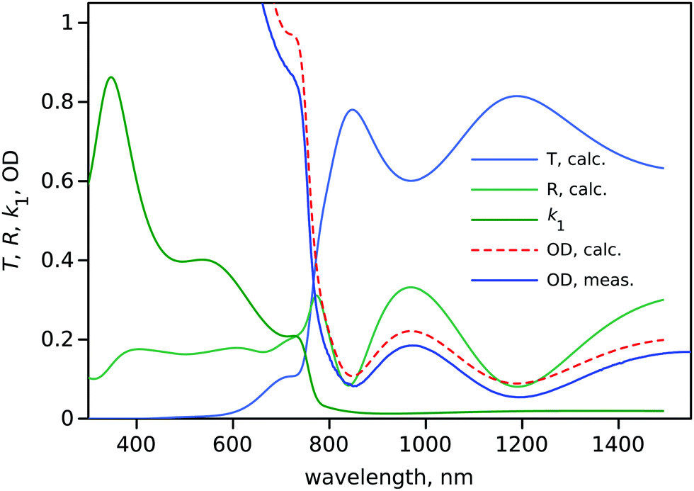 | ||
| Fig. 2 Measured (OD, meas.) and modelled (OD, calc.) absorption spectrum of the perovskite sample, together with the k1 perovskite spectrum used for modelling and modelled transmittance and reflectance spectra. Modelled spectra were calculated for sample thickness d = 524 nm. | ||
3.2 Transient absorption responses in transmittance and reflectance modes
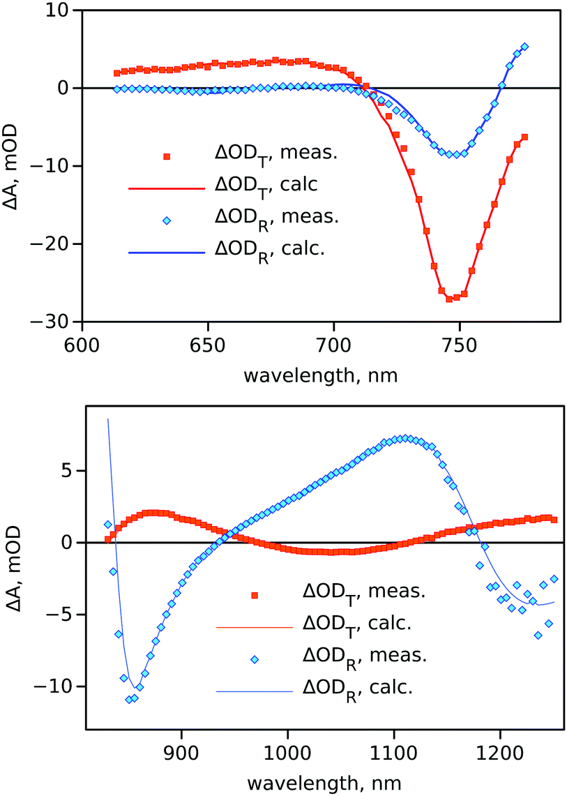
“Standard” pump–probe measurements of the sample with reasonably low excitation density (see ESI,† Fig. S2 for the excitation density dependence measurements) resulted in a rather simple response as presented in Fig. 3. The main signal is a bleaching signal at the edge of the band gap close to 750 nm. There is a slight change in the transient absorption spectrum shape in a few hundreds of femtoseconds usually attributed to thermal relaxation of the photo-generated carriers to the bottom of the conduction band. However, from 1 ps till 1 ns the response remains virtually unchanged. This is a very typical behaviour of this type of metal halide perovskite film.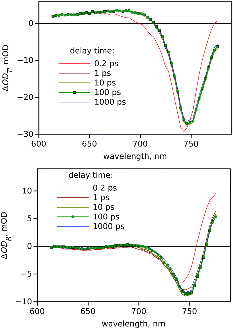 | ||
| Fig. 3 Time resolved transient absorption spectra of the perovskite layer measured in the band gap wavelength region in transmittance (top) and reflectance (bottom) modes. Delay times are indicated in the plots, and the spectrum at 100 ps delay is used for further analysis. | ||
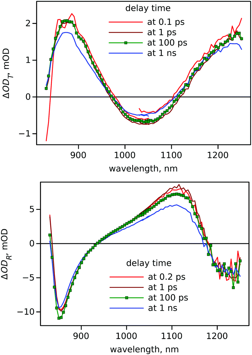
NIR pump–probe responses bring a surprise in transmittance mode – we see a negative signal in the range where the sample has no ground state absorption nor emission (Fig. 4). Otherwise similarly to the visible part of the spectrum the TA signal is formed almost instantly and there is virtually no change till 1 ns delay time.
 | ||
| Fig. 4 Time resolved transient absorption spectra of the perovskite layer in the NIR part of the spectrum obtained in transmittance (top) and reflectance (bottom) modes. The delay times are indicated in the plots. | ||
The “negative” absorption in the 1000–1100 nm range cannot be explained by the change in absorption since this wavelength range is below the band gap. It is also important to recall the wavy shape of the absorption spectrum in this region and notice that the “wave” in the transient absorption is shifted relative to that in the steady state.
The most reasonable explanation of the observed phenomenon is change of reflectance caused by the photo-induced change of the refractive index. To check this hypothesis the measurements were repeated with detection of the reflected light instead of transmitted. The results of the measurements are shown in Fig. 4. The response spectrum shape is also “wavy” and to some extent it is complementary to that obtained in transmittance mode, as expected.
3.3 Calculations of refractive index change (real and imaginary parts)
The spectra Δn1(λ) and Δk1(λ) at a given delay time t can be calculated using eqn (6) and (7). The input parameters for the calculations are the pair of corresponding measured spectra ΔODT(λ) and ΔODR(λ) (Fig. 4), model spectra n1(λ), k1(λ) and n2(λ), and perovskite layer thickness d. In our calculations we used d as a fit parameter to obtain continuous spectra Δn1(λ) and Δk1(λ). The results of calculations for data at 100 ps delay time are presented in Fig. 5, for which the best thickness d was set to 522.4 and 520.6 nm for the visible and NIR parts of the spectrum, respectively. It has to be noted that Δk1 is a dimensionless value and the absorption coefficient change can be calculated as α1 = 2πk1/λ, and Δα1 = 2πΔk1/λ, respectively.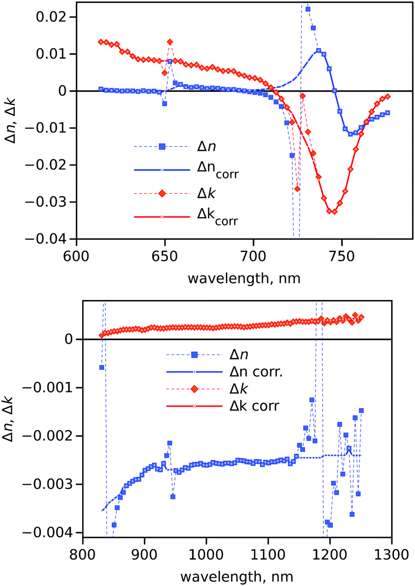 | ||
| Fig. 5 The photo-induced change of n1 and k1 at 100 ps delay time. The spectra calculated directly from the experimental results are shown by symbols connected by fine dashed lines, and smoothed spectra used for further modelling (see text for details) are shown by solid lines with fine marks. | ||
First of all, the calculations show only a small increase in absorption (Δk1) in the NIR part, as can be expected. Secondly, the transient response in the NIR is mostly determined by the change in the refractive index, which is at the level Δn1 ≈ 0.003 at the excitation density used. The contribution of the absorption change is rather minor, Δk1 ≈ 0.0002, which corresponds to the absorption coefficient change of Δα1 ≈ 0.001 μ−1, or the sample absorbs ≈0.05% more light in the excited state than in the ground state.
In the visible part calculations bring no surprises as well. Both Δk1(λ) and Δn1(λ) spectra agree well with previously published results14,19,21 and point to a significant contribution of the refractive index change to the experimentally measured probe light intensity change, as was also noted previously.30
The calculated Δk1 in the NIR is fairly small, ≈0.0002, and satisfies well the assumption of a slightly absorbing medium, n12 ≫ k12. In the visible part the relation is also satisfied for the spectral range used, λ > 600 nm, with k12 being a hundred times smaller than n12. However at shorter wavelengths the approximation of a slightly absorbing medium is ill justified.
The Δn1(λ) spectrum has three wavelengths with highest “distortions” in the NIR at roughly 840, 945 and 1185 nm and two wavelengths, 670 and 715 nm, in the visible region (Fig. 5). These are roughly the wavelengths at which the transient reflectance (TR) spectra cross the zero line in the NIR. Inspection of the data revealed that these are the wavelengths at which the determinant for solving eqn (3) and (4) is close to zero and solutions are the least accurate. A solution to the problem can be an approximation of the Δn1 and Δk1 spectra at such wavelengths using the data from nearby wavelengths. Alternatively, one may use a more physically meaningful approach to gather data at these wavelengths, such as using Kramers–Kronig relations which rely on the knowledge of Δn1 and Δk1 outside the wavelengths in question. Since the distortions affect the Δn1 plot more than the Δk1 plot, Δk1 can be used with Kramers–Kronig relations to estimate Δn1 at the distorted wavelengths. The sample thickness d was optimized to reduce distortion at 945 nm in the NIR, though a small variation of d within 1 nm can reduce distortion at 840 or 1185 nm at the expense of larger distortions at other wavelengths. We can also notice that the “optimum” sample thickness, d, used in the NIR and visible region is slightly different, 520.6 and 522.4 nm, respectively. The most probable reason for this is a mismatch between the real spectra of n1(λ) and n2(λ) and the tabular values used for the modelling.
The distortions were smoothed manually to yield spectra shown in Fig. 5 by solid lines. It is interesting to notice that the Δn1(λ) spectrum is much more distorted than Δk1(λ). The corrected (smoothed) spectra Δncorr and Δkcorr in Fig. 5 were used to calculate expected responses (ΔODT and ΔODT) using the same eqn (5). The results of the calculations are presented in Fig. 6 together with the measured data. The correction has only a minor effect on the ΔODT and ΔODT spectra, and the difference between the measured and corrected spectra seems to be within experimental error.
 | ||
| Fig. 6 Measured ΔODT and ΔODR spectra (symbols) and the spectra calculated after smoothing n1 and k1 (lines) as presented in Fig. 5. Experimental data at 100 ps delay time were used. | ||
It has to be noted that, for non-corrected Δn1 and Δk1, back calculations to ΔODT and ΔODT reproduce the measured values exactly since eqn (5) is the exact mathematical conversion from Δn1 and Δk1 to ΔODT and ΔODT and back. In order to better compare our calculations to work previously done by others, we also simulated ΔODT and ΔODT spectra with the standard Fresnel-equation based transfer matrix method31 which is a common method for simulating thin film reflectance and transmittance (see ESI† for details). Fig. 7 shows that thus calculated Δn1 and Δk1 (with smoothing) reproduce the experimental data with reasonable accuracy also in this simulation.
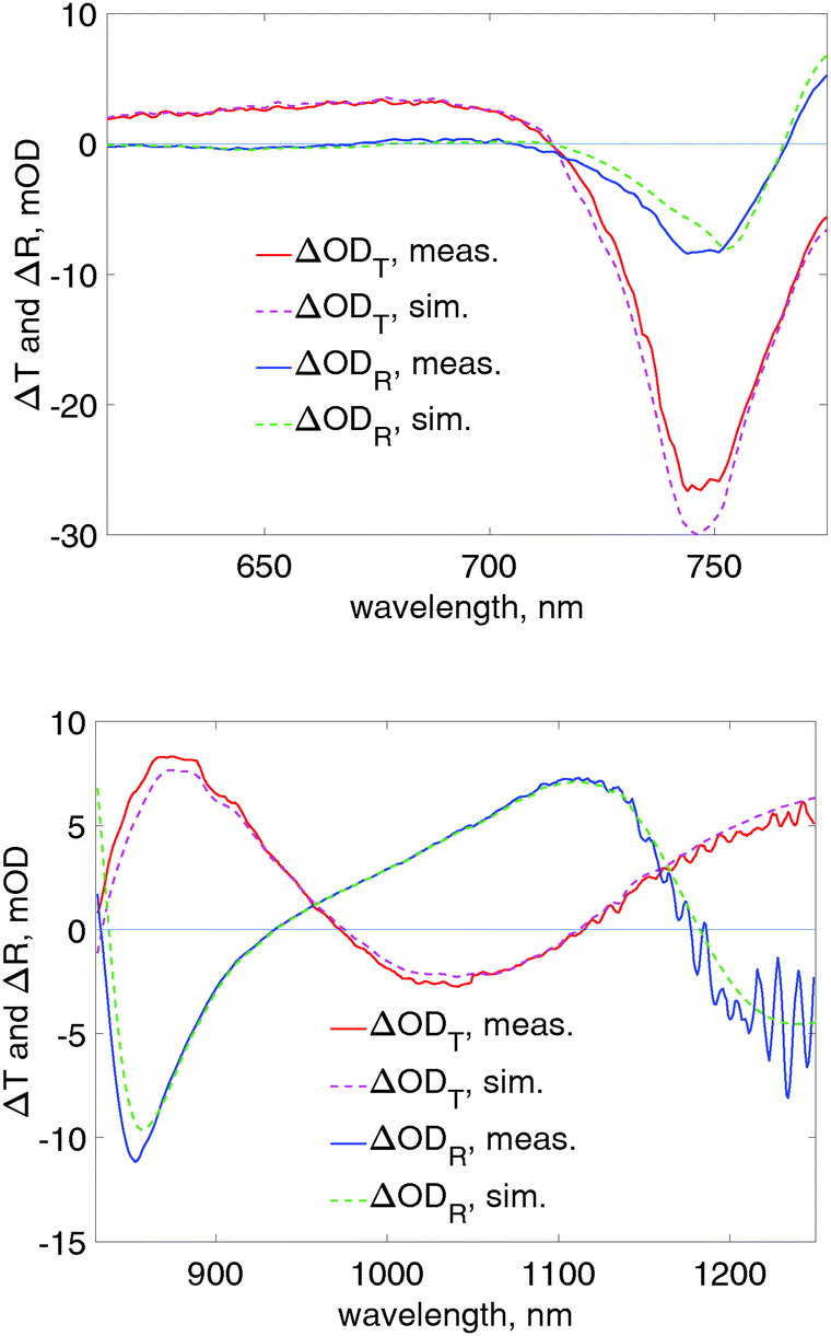 | ||
| Fig. 7 Fresnel-equation based simulation of TA and TR spectra in the visible range (top) and near-infrared (bottom). In the bottom figure ΔODT was multiplied by 4 for clarity. | ||
Our model is limited by the sample structure presented in Fig. 1. We assume here that (1) the photo-active layer, metal halide perovskite, is flat and uniform, and (2) the change in both Δn1 and Δk1 is homogeneous through the hole sample thickness. The latter means that the model is limited to equilibrium photo-carrier distribution through the sample, which is definitely not the case at short delay times and for samples with high optical densities at the excitation wavelength. This was the reason to use an excitation wavelength close to the band-gap and 100 ps delay time in the above analysis as it is believed that at this delay time the carriers are distributed homogeneously enough through the sample to not impact the signal in any significant way. Without these precautions the reflectance may be affected by the non-uniform charge carrier distribution.
The problem of the sample (surface) roughness can be accounted for by splitting the perovskite layer into few layers such as the top rough part and the homogeneous bulk sample. Actually the same approach can be used to account for carrier distribution across the sample created in the samples with high absorbance. This, however, would make the analysis much more complicated and hardly possible if more layers need to be taken into account. The problem is that we need analytical expressions for R and T to calculate derivatives  and so on. The transfer matrix method can be used to simulate the effect of surface roughness on TA and TR responses by splitting the perovskite layer into multiple layers with appropriate n and k. In our simulations we did not find significant difference from having a roughness layer compared to the simple flat layer. Scattering is another problem: although scattering usually doesn’t change upon excitation, it does influence the steady-state measurements and hence makes modelling more difficult.
In application to metal halide perovskite layers, our results show that if only the dynamics of carrier relaxation is of interest, one can do standard measurements in the NIR, select the wavelength of the strongest signal and focus on the time profile of the response. The spectrum of the response is determined by the static refractive index n1 and the sample thickness d, which are not parameters of interest in the case of time resolved measurements. But the signal intensity is proportional to the change of the refractive index which depends on the sample polarizability or the density of free carriers, and thus can be used as a measure of the density of free carriers. An advantage of using NIR monitoring is that there is next to no sample ground state absorption and samples with high absorption in the visible can be studied equally well. However, if one wants to study the absorbance response from a more complex sample than just perovskite, such as electron or hole transport layers (ETL and HTL), then the number of parameters affecting the measurements (refractive indexes and absorption coefficient of other layers) is greater than two and all unknown parameters cannot be extracted from two independent measurements (reflectance and transmittance).
Switching to the reflectance measurement mode had an effect of stronger response and better signal-to-noise ratio in our case. This requires very minor modification of a standard pump–probe instrument. We used a slightly tilted sample and a mirror in front of the sample, which directed the reflected probe light to the detection system. Otherwise the measurement procedure was exactly the same as for the standard pump–probe in transmission mode.
4 Conclusions
Herein we propose an approach which allows us to extract the change in absorption and refractive index from standard transient absorption and reflectance measurements. The method can be applied to any semitransparent photo-active layer with thickness comparable to the wavelength and it accounts for interference of the probe light reflected from two sides of the layer. To apply the method one needs to obtain spectra of the refractive indexes of the studied layer and supporting substrate, and the absorption coefficient of the layer in addition to transient measurements.We applied this technique to study a metal halide perovskite layer for which a few groups have reported recently on the necessity to account for the change in the refractive index when analyzing transient absorption measurements in the band gap wavelength range. Our results support this notion, but we extended the spectral range to the near infrared (NIR) and show that in this range the transient response is determined predominantly by the photo-induced change of the refractive index. After excitation the refractive index decreases and it has mostly a flat spectrum in the range 850–1250 nm. The refractive index depends on the medium polarizability, and its change should follow the change of free carriers in the sample. Therefore transient absorption measurements in the NIR range can be useful to study carrier dynamics, but the spectral features of the response in the NIR are primarily caused by light interference in the thin metal halide perovskite layer.
5 Experimental
FAMACs-perovskite was deposited on soda-lime glass substrates through spin coating.Soda-lime glass substrates (Thermo Scientific™) were washed by sonication for 15 min with Mucasol solution 2% in water, isopropanol and acetone respectively. After 15 min of O3 and ultraviolet (UV) treatment, the samples were taken to a N2-filled glovebox for perovskite spin coating. Regarding the FAMACs-perovskite solution, stock solutions of PbI2 (1.5 M, TCI) and PbBr2 (1.5 M, TCI) in anhydrous dimethylformamide (DMF)/dimethyl sulfoxide (DMSO) = 4![[thin space (1/6-em)]](https://www.rsc.org/images/entities/char_2009.gif) :1 (v:v, Sigma-Aldrich) were previously prepared and heated overnight at 60 °C in a thermoshaker before use. Methylammonium (MA) bromide and formamidinium (FA) iodide powders (dyenamo) were weighed out in two separate vials and then the suitable volume of PbI2 (PbBr2) stock solutions was calculated and added to the vials containing the FAI (MABr) powder to get a stoichiometry of FAI:PbI2 (MABr:PbBr2) of 1:1.09. Before deposition, the solutions were mixed as follows: FAPbI3:MAPbBr3 = 85:15 (v:v). Further CsI (1.5 M, Sigma-Aldrich) from a stock solution in DMSO was eventually added to the precursor solution to produce a final composition with the stoichiometry (CsI)0.05[((MAPbBr3)0.15(FAPbI3)0.85)]0.95. 80 μL of perovskite solution was then drop-cast on the 2.5 × 2.5 cm2 substrate and spin coated in a two-step program at 1000 rpm for 10 s and 6000 rpm for 20 s. 5 s prior to the end of the program, 100 μL of anhydrous chlorobenzene was poured on the spinning substrate. Subsequently, the sample was annealed at 100 °C for 1 h.
:1 (v:v, Sigma-Aldrich) were previously prepared and heated overnight at 60 °C in a thermoshaker before use. Methylammonium (MA) bromide and formamidinium (FA) iodide powders (dyenamo) were weighed out in two separate vials and then the suitable volume of PbI2 (PbBr2) stock solutions was calculated and added to the vials containing the FAI (MABr) powder to get a stoichiometry of FAI:PbI2 (MABr:PbBr2) of 1:1.09. Before deposition, the solutions were mixed as follows: FAPbI3:MAPbBr3 = 85:15 (v:v). Further CsI (1.5 M, Sigma-Aldrich) from a stock solution in DMSO was eventually added to the precursor solution to produce a final composition with the stoichiometry (CsI)0.05[((MAPbBr3)0.15(FAPbI3)0.85)]0.95. 80 μL of perovskite solution was then drop-cast on the 2.5 × 2.5 cm2 substrate and spin coated in a two-step program at 1000 rpm for 10 s and 6000 rpm for 20 s. 5 s prior to the end of the program, 100 μL of anhydrous chlorobenzene was poured on the spinning substrate. Subsequently, the sample was annealed at 100 °C for 1 h.
Ultrafast transient absorption and reflectance responses of the samples were measured in ambient conditions using a pump–probe system described previously.32,33 Briefly, the samples were excited by laser pulses at 600 or 700 nm (Libra F, Coherent Inc., coupled with Topas C, Light Conversion Ltd). A white continuum generator (sapphire crystal) was used to produce the probe beam. The TA responses were measured using an ExciPro TA spectrometer (CDP, Inc.) equipped with a CCD array for the visible spectral range (460–770 nm), and an InGa diode array for the near-infrared wavelengths (measured in two ranges 840–1050 and 1050–1260 nm). The pulse repetition rate of the laser system was 1 kHz and the spectra were typically acquired by averaging over 5 s. Typical time resolution of the instrument was 100 fs. The sample was tilted slightly (roughly 8 degrees) to allow both transmittance and reflectance mode measurements. The transmittance mode measurements were acquired by detecting the probe passing the sample. In the reflectance mode the probe light reflected from the sample was directed to the detection system by a mirror placed in front of the sample. Data collected in the three wavelength ranges were fitted globally to a sum of exponential functions. The fit program accounted for the instrument response (through a de-convolution process) and did the group velocity dispersion compensation.
Conflicts of interest
There are no conflicts to declare.Acknowledgements
The work is part of the Academy of Finland Flagship Programme, Photonics Research and Innovation (PREIN), decision 320165. Paola Vivo and Hannu P. Pasanen thank the Jane & Aatos Erkko foundation (project ASPIRE) and the doctoral program of Tampere University for financial support. Financial support from Business Finland/Forschungszentrum Jülich GmbH (SolarWAVE project) is also gratefully acknowledged.Notes and references
- NREL, Best Research-cell Efficiency Chart, https://www.nrel.gov/pv/assets/pdfs/best-reserch-cell-efficiencies.pdf, Accessed: April 15, 2019.
- N.-G. Park, M. Grätzel, T. Miyasaka, K. Zhu and K. Emery, Nat. Energy, 2016, 1, 16152 CrossRef CAS.
- A. Jena, A. Kulkarni and T. Miyasaka, Chem. Rev., 2019, 119, 3036–3103 CrossRef CAS PubMed.
- K. Lin, J. Xing, L. Quan, F. P. G. de Arquer, X. Gong, J. Lu, L. Xie, W. Zhao, D. Zhang, C. Yang, W. Li, X. Liu, Y. Lu, J. Kirman, E. Sargent, Q. Xiong and Z. Wei, Nature, 2018, 562, 245–248 CrossRef CAS PubMed.
- B. Zhao, S. Bai, V. Kim, R. Lamboll, R. Shivanna, F. Auras, J. Richter, L. Yang, L. Dai, M. Alsari, X.-J. She, L. Liang, J. Zhang, S. Lilliu, P. Gao, H. Snaith, J. Wang, N. Greenham, R. Friend and D. Di, Nat. Photonics, 2018, 12, 783–789 CrossRef CAS.
- K. Wang, S. Wang, S. Xiao and Q. Song, Adv. Opt. Mater., 2018, 6, 1800278 CrossRef.
- X. Wang, M. Li, B. Zhang, H. Wang, Y. Zhao and B. Wang, Org. Electron., 2018, 52, 172–183 CrossRef CAS.
- F. Yao, P. Gui, Q. Zhang and Q. Lin, Mol. Syst. Des. Eng., 2018, 3, 702–716 RSC.
- L. Herz, ACS Energy Lett., 2017, 2, 1539–1548 CrossRef CAS.
- S. Stranks, G. Eperon, G. Grancini, C. Menelaou, M. Alcocer, T. Leijtens, L. Herz, A. Petrozza and H. Snaith, Science, 2013, 342, 341–344 CrossRef CAS PubMed.
- M. Li, B. Wu and T.-C. Sum, The photophysics of halide perovskite solar cells, Wiley-VCH Verlag GmbH Co. KGaA, Germany, 2019 Search PubMed.
- M. Johnston and L. Herz, Acc. Chem. Res., 2016, 49, 146–154 CrossRef CAS PubMed.
- J. Shi, Y. Li, Y. Li, D. Li, Y. Luo, H. Wu and Q. Meng, Joule, 2018, 2, 879–901 CrossRef CAS.
- R. R. Tamming, J. Butkus, M. B. Price, P. Vashishtha, S. K. K. Prasad, J. E. Halpert, K. Chen and J. M. Hodgkiss, ACS Photonics, 2019, 6, 345–350 CrossRef CAS.
- Y. Yang, Nat. Photonics, 2016, 10, 53–59 CrossRef CAS.
- K. G. Stamplecoskie, J. S. Manser and P. V. Kamat, Energy Environ. Sci., 2015, 8, 208–215 RSC.
- O. Flender, J. R. Klein, T. Lenzer and K. Oum, Phys. Chem. Chem. Phys., 2015, 17, 19238–19246 RSC.
- G. Grancini, D. Viola, Y. Lee, M. Saliba, S. Paek, K. Cho, S. Orlandi, M. Cavazzini, F. Fungo, M. Hossain, A. Belaidi, N. Tabet, G. Pozzi, G. Cerullo and M. Nazeeruddin, ChemPhysChem, 2017, 18, 2381–2389 CrossRef CAS PubMed.
- M. B. Price, J. Butkus, T. C. Jellicoe, A. Sadhanala, A. Briane, J. E. Halpert, K. Broch, J. M. Hodgkiss, R. H. Friend and F. Deschler, Nat. Commun., 2015, 6(8420), 1–8 Search PubMed.
- J. Werner, G. Nogay, F. Sahli, T. C.-J. Yang, M. Bräuninger, G. Christmann, A. Walter, B. A. Kamino, P. Fiala, P. Löper, S. Nicolay, Q. Jeangros, B. Niesen and C. Ballif, ACS Energy Lett., 2018, 3, 742–747 CrossRef CAS.
- T. Ghosh, S. Aharon, A. Shpatz, L. Etgar and S. Ruhman, ACS Nano, 2018, 12, 5719–5725 CrossRef CAS PubMed.
- Y. Yang, Y. Yan, M. Yang, S. Choi, K. Zhu, J. Luther and M. Beard, Nat. Commun., 2017, 6, 7961 CrossRef PubMed.
- M. Park, A. J. Neukirch, S. E. Reyes-Lillo, M. Lai, S. R. Ellis, D. Dietze, J. B. Neaton, P. Yang, S. Tretiak and R. A. Mathies, Nat. Commun., 2018, 9, 2525 CrossRef PubMed.
- P. Piatkowski, B. Cohen, F. J. Ramos, M. D. Nunzio, M. K. Nazeeruddin, M. Grätzel, S. Ahmad and A. Douhal, Phys. Chem. Chem. Phys., 2015, 17, 14674–14684 RSC.
- A. Barybin and V. Shapovalov, Int. J. Opt., 2010, 137572 Search PubMed.
- M. Saliba, J.-P. Correa-Baena, C. M. Wolff, M. Stolterfoht, N. Phung, S. Albrecht, D. Neher and A. Abate, Chem. Mater., 2018, 30, 4193–4201 CrossRef CAS.
- M. Saliba, T. Matsui, J.-Y. Seo, K. Domanski, J.-P. Correa-Baena, M. K. Nazeeruddin, S. M. Zakeeruddin, W. Tress, A. Abate, A. Hagfeldtd and M. Grätzel, Energy Environ. Sci., 2016, 9, 1989–1997 RSC.
- J. A. Christians, P. Schulz, J. S. Tinkham, T. H. Schloemer, S. P. Harvey, B. J. T. de Villers, A. Sellinger, J. J. Berry and J. M. Luther, Nat. Energy, 2018, 3, 68–74 CrossRef CAS.
- L. J. Phillips, A. M. Rashed, R. E. Treharne, J. Kay, P. Yates, I. Z. Mitrovic, A. Weerakkody, S. Hall and K. Durose, Data Brief, 2015, 5, 926–928 CrossRef PubMed.
- J. Liu, J. Leng, S. Wang, J. Zhang and S. Jin, J. Phys. Chem. Lett., 2019, 10, 97–101 CrossRef CAS PubMed.
- A. Yariv and P. Yeh, Photonics: Optical Electronics in Modern Communications, Oxford University Press, 6th edn, 2007 Search PubMed.
- K. Virkki, S. Demir, H. Lemmetyinen and N. V. Tkachenko, J. Phys. Chem. C, 2015, 119, 17561–17572 CrossRef CAS.
- K. Stranius, L. George, A. Efimov, T.-P. Ruoko, J. Pohjola and N. V. Tkachenko, Langmuir, 2015, 31, 944–952 CrossRef CAS PubMed.
Footnote |
| † Electronic supplementary information (ESI) available: Method details for Δn and Δk calculations and transfer matrix based simulations, including a steady-state transmittance and reflectance simulation. ESI also has an example of primary TA absorption measurements and TA decay profiles and different excitation intensities. See DOI: 10.1039/c9cp02291k |
| This journal is © the Owner Societies 2019 |