
 Open Access Article
 This Open Access Article is licensed under a
 Creative Commons Attribution 3.0 Unported Licence
Enhancing the electrocatalytic activity of 2H-WS2 for hydrogen evolution via defect engineering†
Longfei
Wu
 a,
Arno J. F.
van Hoof
a,
Nelson Y.
Dzade
b,
Lu
Gao
a,
Marie-Ingrid
Richard
cd,
Heiner
Friedrich
e,
Nora H.
De Leeuw
b,
Emiel J. M.
Hensen
a and
Jan P.
Hofmann
*a
a,
Arno J. F.
van Hoof
a,
Nelson Y.
Dzade
b,
Lu
Gao
a,
Marie-Ingrid
Richard
cd,
Heiner
Friedrich
e,
Nora H.
De Leeuw
b,
Emiel J. M.
Hensen
a and
Jan P.
Hofmann
*a
aLaboratory for Inorganic Materials and Catalysis, Department of Chemical Engineering and Chemistry, Eindhoven University of Technology, P.O. Box 513, 5600 MB Eindhoven, The Netherlands. E-mail: J.P.Hofmann@tue.nl
bFaculty of Geosciences, Utrecht University, P.O. Box 80.021, 3508 TA Utrecht, The Netherlands
cAix Marseille Université, CNRS, Université de Toulon, IM2NP UMR 7334, 13397 Marseille, France
dID01/ESRF, The European Synchrotron, 71 rue des Martyrs, 38043 Cedex Grenoble, France
eLaboratory of Materials and Interface Chemistry, Department of Chemical Engineering and Chemistry, Eindhoven University of Technology, P.O. Box 513, 5600 MB Eindhoven, The Netherlands
First published on 21st February 2019
Abstract
Transition metal dichalcogenides (TMDs), such as MoS2 and WS2, are promising alternative non-noble metal catalysts to drive the electrocatalytic H2 evolution reaction (HER). However, their catalytic performance is inherently limited by the small number of active sites as well as their poor electrical conductivity. Here, we grow vertically aligned 2H-WS2 on different substrates to expose their edge sites for the HER and introduce a scalable approach to tune these active sites via defect engineering. In a thermal hydrogen treatment procedure, sulfur vacancies and metallic tungsten nanoparticles are formed. The extent of desulfurization, and thus the HER activity, can be tuned via controlling the H2 annealing conditions. The obtained W/WS2−x electrocatalysts are evaluated experimentally and theoretically to arrive at a better understanding of how to modify the inherently inert 2H-WS2 for more efficient HER.
Introduction
The growing demand for energy has stimulated global efforts to explore renewable energy sources such as wind and solar. However, efficient energy storage to solve the issue of their intermittency remains to be solved.1–4 Hydrogen is arguably the most promising alternative fuel due to its cleanness, renewability, and high gravimetric energy density.5 Hydrogen production via electrochemical water splitting (hydrogen evolution reaction, HER) has been emerging as a promising sustainable approach.6 The key challenge for enabling this process at a large scale is the development of efficient, durable and low cost electrocatalysts for HER. Currently, platinum-based materials serve as the benchmark catalysts for HER due to their high catalytic activity;7 yet, the scarcity and cost of Pt significantly hamper their widespread application.2,8 Transition metal dichalcogenides (TMDs) with two-dimensional (2D)-layered crystal structures, such as MoS2 and WS2, have been extensively used as HER catalysts.9 Both experimental6 and computational10 studies show comparable catalytic activity with commercial Pt/C composites, as such potentially rivalling state-of-the-art catalysts in electrochemical or photoelectrochemical cells.9,11Although the (0001) basal planes of semiconductor phase TMDs (2H-TMDs) are not active HER catalysts, the edge sites of 2H-TMDs were theoretically predicted12 and experimentally13 verified to be active for HER. Many efforts have been devoted to maximally expose those edge sites by various methods such as nano-structuring,13 size-controlling,14 and defect engineering.15,16 However, the guiding principle for all these approaches usually has been to optimize the active sites rather than tailor the inert basal planes because the edge sites have been identified to be HER active exhibiting a similar Gibbs free energy for atomic hydrogen adsorption (ΔGH) as the most active Pt-group metals.17 Specifically for MoS2, extensive efforts have been devoted in developing feasible ways for engineering higher densities of active sites.18 As to the edge sites of 2H-TMDs, only pure metal edges or metal edges passivated with S-monomers are preferably favorable for HER, whereas the configuration with full S-passivation (S-dimers) is too inert for these relevant catalytic reactions to occur.19,20 Thus, active sites can be created on either the (0001) basal plane of 2H-TMDs or at the inert S-dimer edges. Tsai and co-workers demonstrate an electrochemical process for generating S-vacancies in monolayer and polycrystalline MoS2 to tune the HER activity.21 Cheng et al. reported a remote hydrogen-plasma process to create sulfur vacancies on the basal plane of monolayer crystalline TMDs while maintaining the pristine morphology and structure.22 Aside from desulfurization, other studies report on maximizing the number of exposed active metal sites to achieve an enhancement for HER activity. Woods et al.23 and Wang et al.24 present a unique vertically aligned MoS2 and MoS2/WS2 structure with exposed metal edge sites which show notable HER activity. This prominent improvement in activity was ascribed to the distinct vertical structure maximizing the exposure of catalytically active sites. Other approaches such as thermal annealing25 or ball milling26 were also applied to tune the HER activity of TMDs. However, even though a lot of efforts have been devoted to developing versatile methods to tune the structure of 2H-TMDs and to increase the number of HER active sites, deeper understanding of the structural evolution during treatment (for instance, texturization25 and desulfurization26) processes and how to correlate structural changes to HER activity needs to be developed.
Here, we have selected WS2 as a platform to induce more active HER sites in the 2H phase via a controllable and effective thermal H2 treatment procedure. Vertically aligned 2H-WS2 was grown on various substrates (SiO2/Si, Si3N4 and carbon fiber paper) using sulfurization of sputter-deposited metal tungsten. By annealing in a hydrogen atmosphere, sulfur vacancies and tungsten nanoparticles were formed which are supposed to act as active sites for HER. Further hydrogen treatment yielded a highly defective tungsten sulfide (WS2−x). In addition, extended H2 annealing led to a complete change of the initial structure and emergence of new morphologies such as nanotubes and porous structures. The as-derived highly defective WS2−x shows prominent HER activity compared to the pristine 2H-WS2 and reported tungsten sulfide materials in the literature. A detailed nanostructure analysis has been conducted on the highly defective WS2−x, applying XPS, HR-TEM, HAADF-STEM and synchrotron-based nano-focus XRD to shed light on the observed significant improvement in HER activity.
Experimental
Materials synthesis
2H-WS2 films were prepared via sulfurization of sputtered metal tungsten on different substrates in a thermal chemical vapor deposition (CVD) system (Fig. S1, ESI†).27 Specifically, SiO2 (300 nm)/Si sputter-coated with 20 nm W was placed at the center of a tube furnace. After loading 500 mg (99.98%, Aldrich) sulfur powder at the upstream, the tube was sealed, evacuated and refilled with N2 three times to remove O2 in the system. Then, the tube was flowed with Ar (100 sccm) for 15 min. Afterwards, the furnace was heated up with a heating rate of 20 °C min−1 and kept for 15 min at the target temperature (600 °C). The sulfur powder was heated to 170 °C accordingly. Defective tungsten sulfide was prepared by a post-synthetic treatment under similar conditions. The sulfur source was cooled down and subsequently H2 with certain flow rate was introduced at the target temperature. Samples for transmission electron microscopy (TEM) analysis were prepared on custom-made TEM grids (Lionix BV) which consist of a silicon frame and a central part that was etched away to create a 15–20 nm thick silicon nitride membrane window (100 × 100 μm2) where the electron beam can pass.28–31 Prior to tungsten sputtering, the TEM grids were calcined in dry air to form a 3 nm thick surface layer of silicon oxide.28Characterization
X-ray photoelectron spectroscopy (XPS) was recorded on a Thermo Scientific K-Alpha instrument equipped with a monochromatic X-ray source (hν(Al Kα) = 1486.6 eV). Binding energy calibration was performed by using the sp3 C 1s peak of adventitious carbon at 284.6 eV as reference. Spectra were fitted by Casa XPS software. Raman spectra measurements were performed on a Renishaw Raman InVia microscope equipped with a 514 nm laser, integrated switchable gratings with 600 or 1800 lines per mm, and a CCD detector. For each scan, 5 accumulations with acquisition time of 10 s were taken. TEM images were acquired with a FEI Tecnai 20 transmission electron microscope equipped with a LaB6 filament and operated at an acceleration voltage of 200 kV. High resolution TEM (HR-TEM) and high angle annular dark field scanning transmission electron microscopy (HAADF-STEM) imaging were performed at room temperature on a FEI CryoTitan transmission electron microscope which is equipped with a field emission electron gun and operated at 300 kV. HR-TEM and select area electron diffraction (SAED) images were acquired using a Gatan 2K CCD camera. STEM images were acquired using a probe convergence angle of 10 mrad, a dwell time of 2 μs and a camera length of 115 mm in combination with a Fischione HAADF detector. Nano X-ray diffraction analysis was performed at the European Synchrotron (ESRF) at the ID01 X-ray diffraction and scattering beamline with beam energy of 8.0 keV and beam size of 100 × 400 nm2. Energy dispersive X-ray spectroscopy (EDX) was obtained on a Phenom ProX scanning electron microscope with 5 kV acceleration voltage. Grazing incidence X-ray diffraction (GI-XRD) measurement was performed on a Panalytical X Pert PRO MRD employing Cu Kα (1.54 Å) radiation with an incidence angle of 0.5° with respect to the substrate plane. Near Ambient Pressure XPS (NAP-XPS) was conducted on a SPECS system with a PHOIBOS 150 NAP hemispherical energy analyzer in 5 mbar H2 pressure at 600 °C.Electrochemical measurements
Electrochemical measurements were performed in a three-electrode electrochemical cell with saturated calomel electrode (SCE) (0.269 V vs. reversible hydrogen electrode (RHE)) as the reference electrode, Pt foil (1 × 2 cm2) as the counter electrode, and 0.5 M H2SO4 (99.999%, Sigma-Aldrich) as electrolyte. The electrolyte was prepared with 18 MΩ cm deionized Milli-Q water and purged with Ar for 20 min to remove O2 in the solution prior to the measurements. Cyclic voltammetry and linear sweep voltammetry curves were recorded on a Metrohm Autolab PGSTAT302N potentiostat, and current density values are normalized by geometric area. IR correction has been done before normalization on geometric area. AC electrochemical impedance spectroscopy (amplitude: 10 mV) was recorded at open circuit potential (OCP) in the frequency range of 100 kHz to 1 Hz. Stability tests were conducted by recording chronopotentiostatic responses with glassy carbon as a counter electrode to exclude possible contamination by Pt.Results and discussion
Reduced WS2−x as catalyst for HER
The synthesis method to prepare defective tungsten sulfide is schematically depicted in Fig. 1a. Elemental W films (20 nm) were deposited on a SiO2 (300 nm)/Si ((100) orientation, type: P/B, resistivity: 0–100 Ohm cm) substrate by magnetron sputtering, then reacted with sulfur, as described in the experimental section to produce WS2. Fig. 1b shows a typical TEM image of a WS2 film revealing the presence of vertically aligned layers with an inter-layer spacing of ∼0.67 nm.32 Grazing-incidence X-ray diffraction (Fig. S2, ESI†) indicates a strong peak at 2θ = 14.12° which corresponds to the (002) reflection (interlayer spacing = 0.67 nm) of the semiconducting 2H phase of WS2.32.33 The as-prepared 2H-WS2 was annealed at 600 °C with 10% H2 concentration (total flow: 100 sccm, Ar as balance) for 6 h to remove sulfur atoms and produce metal sites or clusters. The TEM image in Fig. 1c shows that nanoparticles with an average size of 3 nm were formed on the film along with an overall sulfur/tungsten (S/W) ratio of 1.82 as obtained by X-ray photoelectron spectroscopy (XPS, Fig. 2). Interestingly, when we further prolonged the H2 annealing time to 10 h, the initial vertical structure turned into new structures such as multi-walled WS2−x nanotubes (lattice spacing: 0.67 nm) with an outer diameter of 10–17 nm (Fig. 1d and Fig. S4, ESI†),34–36 along with a decrease of the S/W ratio to 0.37. | ||
| Fig. 1 (a) Scheme showing the transformation of WS2 to W/WS2−x upon annealing in H2 atmosphere; (b) TEM images of pristine WS2.08, inset: lattice spacing obtained from HRTEM; (c) TEM image of WS1.82 obtained via annealing in 10% H2 at 600 °C for 6 h, arrows indicate the formation of nanoparticles, inset: lattice spacing obtained from HRTEM; (d) TEM image of WS0.37 obtained via H2 annealing (10%) at 600 °C for 10 h, inset: lattice spacing obtained from HRTEM; (e) size distribution of W nanoparticles for WS1.82 obtained from the TEM image shown in (c). | ||
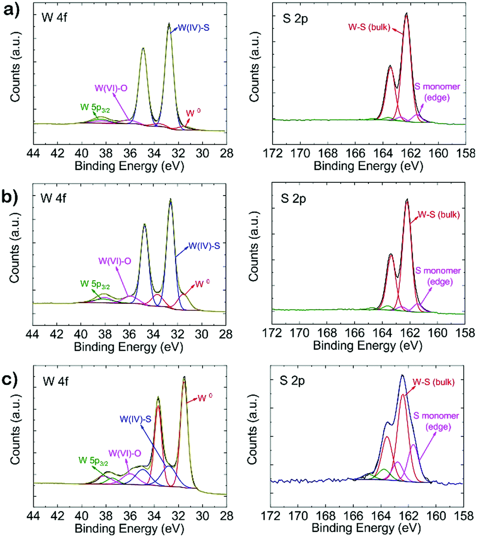 | ||
| Fig. 2 W 4f and S 2p XP spectra of pristine WS2.08 (a), WS1.82 (b) and WS0.37 (c). | ||
A detailed XPS analysis of the different tungsten sulfide samples is shown in Fig. 2. The W 4f spectrum can be deconvoluted into four components. The peak at 38.6 eV corresponds to W 5p3/2. Two characteristic peaks of WS2 centered at 32.7 eV (W 4f7/2) and 34.9 eV (W 4f5/2) are observed, while the high binding energy peak at 36.1 eV corresponds to the W 4f7/2 component of WO3 which might be due to a slight oxidation of the films resulting from sample handling in air.14,37,38 Aside from the decreasing S/W ratio, the obvious increase of the W 4f7/2 peak at 31.4 eV demonstrates that metallic phase W0 has been produced. This is substantiated by the S 2p XP spectra. Here, except for the main doublet centered at binding energies of 162.3 and 163.4 eV corresponding to the S 2p3/2 and S 2p1/2 components of WS2, respectively, the increase of sulfur monomer (edge) species at 161.5 eV (2p3/2) and 162.6 eV (2p1/2) also indicates that more W–S (bulk) bonds were broken generating more sulfur monomers.19 To assess the progressing reduction of WS2, we applied Near Ambient Pressure (NAP)-XPS to monitor in situ changes in S and W speciation during annealing in a H2 atmosphere. Fig. S3 (ESI†) shows that the S/W ratio decreases from 2.89 to 1.91 within two hours of H2 treatment at 600 °C under 5 mbar H2 pressure.
The as-prepared vertically aligned and defective tungsten sulfide is further characterized by Raman spectroscopy.39Fig. 3 shows the normalized Raman spectra of tungsten sulfide with stoichiometric ratio (WS2.08), treated with H2 annealing (WS1.80, WS1.62), and highly defective WS0.37 after prolonged hydrogen treatment. The peaks at ∼355 and 420 cm−1 are assigned to the first-order modes at the Brillouin zone center of E12g (Γ) (in plane vibration phonon mode) and A1g (Γ) (out-of-plane vibration phonon mode) of 2H-WS2 respectively.32
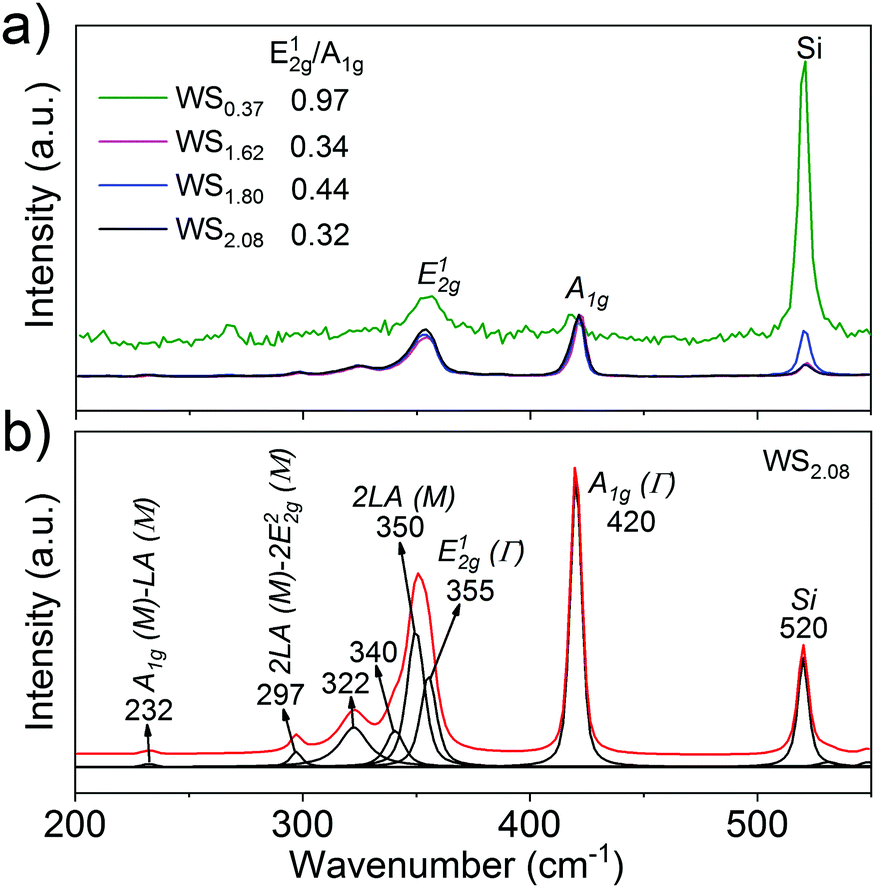 | ||
| Fig. 3 (a) Raman spectra (normalized on the A1g peak) of tungsten sulfide films prepared on SiO2/Si substrates; (b) fitted (Gaussian–Lorentzian) spectra of WS2.08. | ||
Other small features at ∼297 and ∼232 cm−1 are assigned to the second longitudinal acoustic mode (2LA (M)) of 2 E22g and A1g (M)–LA (M) respectively, which are consistent with those observed in the literature.32,40–42 One unique feature observed in our Raman spectra is that the intensity ratio of E12g/A1g is below unity for stoichiometric and less defective tungsten sulfide, which indicates a prominent out-of-plane vibration (A1g) over the in-plane vibration (E12g) mode. The small E12g/A1g ratio indicates a more pronounced presence of vertically aligned layers which is consistent with the TEM results in Fig. 1b.31,39,41 However, for highly defective tungsten sulfide (WS0.37), the Raman intensity of the material was significantly weakened along with an increase of the E12g/A1g ratio to 0.97. The former indicates that the crystallinity of the tungsten sulfide films has decreased, while the latter points to a progressing loss of vertical alignment under the applied harsh reduction conditions.
The as-prepared tungsten sulfide films were investigated as electrocatalysts for HER in a standard three-electrode electrochemical cell in 0.5 M H2SO4 electrolyte. Fig. 4 displays the linear sweep voltammetry (LSV) curves of tungsten sulfide films with various S/W ratios. With decreasing S/W ratio, the LSV curves demonstrate higher current density and the Tafel slope decrease accordingly, which means that the increase of sulfur vacancies and the presence of metal sites contribute to the improvement of HER activity. Despite the increase of tungsten oxide species detected by XPS with decreasing S/W ratio, we do not observe any notable reduction peaks in the CV curves (Fig. S7, ESI†), which suggests that the defective tungsten sulfide films are stable in acid media.38
 | ||
| Fig. 4 (a) Linear sweep voltammetry curves of tungsten sulfide obtained with different S/W ratios in 0.5 M H2SO4. Scan rate: 5 mV s−1. (b) Tafel slopes obtained from LSV curves in (a). | ||
To further investigate the local crystal structure and phase composition of defective tungsten sulfide, TEM images with corresponding selected area electron diffraction (SAED) patterns as well as HAADF-STEM are displayed for WS0.95 in Fig. 5. This sample was directly prepared on a TEM grid and annealed at 600 °C with 10% H2, where a and b represent two typical regions on the grid. In Fig. 5a and b, the TEM image of (a1) shows that the majority of the vertically aligned layered structure is well maintained except for some nanoparticles, which can be either metal W or sulfur as residue from the sulfurization process; (b0) and (b1) display a region where most of the aligned lamellar structure is destroyed and a lot of holes and pits on a sub-μm scale have appeared (bright in BF-TEM (a0, b0), dark in HAADF-STEM (a1, b1)) across the film. The significant morphological difference in these two regions of the same sample led us to further investigate their crystal structures. The appearance of rings in the SAED patterns indicates the presence of multiple crystalline orientations with respect to the electron beam within the probed area, highlighting the polycrystalline nature of the regions a1 and b1 (Fig. 5). The radial average of the SAED patterns obtained in both regions is plotted in Fig. 5c. For comparison, standard diffraction data for W (dark yellow, JCPDS card number: 01-1203) and WS2 (green, JCPDS card number: 08-0237) are included. Interestingly, both W and WS2 are present (Fig. 5c) in regions a and b, while region a has less W content compared to that of region b based on W(110), (211), (310) etc. At lower magnifications in STEM, the defective tungsten sulfide can be clearly divided into a WS2-rich and W-rich zone, respectively, which can be a result of non-uniformity across the film during the H2 treatment process. Moreover, we conducted synchrotron-based nano-focus X-ray diffraction to examine the local crystal structure in small sample areas. The co-existence of W and WS2 on a sub-μm scale (100 × 400 nm2) is evident; results are shown in Fig. S15 (ESI†), where clear W(110) reflections at 2θ = 40.2° could be observed next to reflections of WS2. In order to complete the microstructural analysis, we have conducted SEM and EDX mapping measurements to check the morphology and distribution of elements on the μm scale. The pinholes (dark regions) shown in SEM images obtained with a back-scattered electron detector (BSE) (Fig. S16a, ESI†) are caused by nano-structuring during the H2 treatment process. The merged EDX mapping of O and S indicates that there is a slight oxidation of the film.
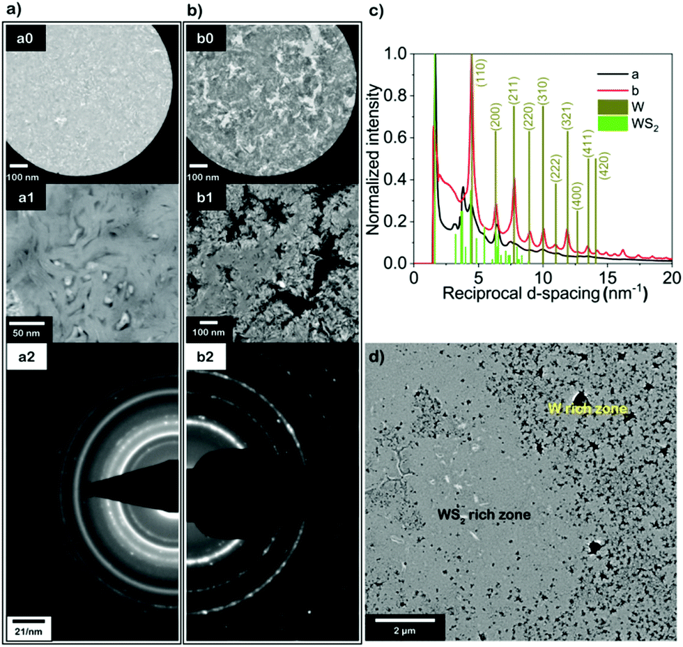 | ||
| Fig. 5 (a and b) Selected area bright field TEM (BF-TEM) images (a0 and b0) and HAADF-STEM images (a1 and b1) of WS0.95, (a) and (b) corresponding to different regions of the sample, typical selected area electron diffraction (SAED) patterns of (a1) and (b1) are shown in (a2) and (b2), respectively; (c) radially averaged SAED signal for (a1) (black curve) and (b1) (red curve); (d) low magnification STEM image of WS0.95. | ||
Comparison with metallic W
We also compared HER activities of the highly defective tungsten sulfide (WS0.37) with sputtered metallic tungsten (Fig. S5, ESI†). Remarkably, WS0.37 shows both lower onset potential and much higher current density than those of sputtered W. The enhanced HER activity is further illustrated by comparing the Tafel slopes (Fig. S5d, ESI†), where WS0.37 exhibits a smaller value of 77 mV per decade (without uncompensated resistance correction) as compared to sputtered W (145 mV per decade). Additionally, Nyquist plots shown in Fig. S5c (ESI†) indicate that the impedance of W is almost three times higher than that of WS0.37 (83 Ω for W and 32 Ω for WS0.37), which is ascribed to the serious surface oxidation of sputtered W (Fig. S6, ESI†). The earlier onset of catalytic activity and lower Tafel slope of highly defective tungsten sulfide suggest that the free binding energy of hydrogen to WS0.37 is much closer to equilibrium than stoichiometric WS2 and metallic W.Influence of H2 annealing temperature
To evaluate the influence of annealing temperature on the structure and activity change of 2H-WS2, we treat the as-prepared films at 700 °C in 10% H2 for different time. Fig. S8 (ESI†) shows the XP spectra of defective tungsten sulfide obtained at 700 °C indicating that the S/W ratio decreases from 2.07 to 1.18 after 1.5 h H2 treatment and further decreases to 0.17 after 3 h. As mentioned before, the presence of sulfur monomer (edge) species at BE(S 2p3/2) = 161.5 eV is an indication of the breaking of W–S (bulk) bonds. The increasing proportion of this kind of sulfur bond further evidences the generation of more defect sites. The morphology of defective tungsten sulfide prepared at 700 °C was also studied by TEM shown in Fig. S9 (ESI†). The vertically aligned layered WS2 evolves into an irregular defect-rich structure with long tubes after 1 h H2 treatment at 700 °C, whereas the tubes disappear and more defects are generated with longer annealing time. Further Raman characterization (Fig. S10, ESI†) shows that the intensity of the E12g and A1g peaks gradually decreases with increasing H2 annealing time, which is further evidence of the increasing loss of crystallinity. Electrochemical tests were performed on the aforementioned tungsten sulfide films to evaluate their HER activity. The CV and LSV curves in Fig. S11 (ESI†) demonstrate a dramatic increase of the current density and lower onset potential for films treated at 700 °C in 10% H2 for 0.5 to 3 h compared with pristine WS2. Surprisingly, further extension of H2 annealing at 700 °C to 6 h shows a much lower HER activity compared with H2 treatment for 3 h. Such a trend is also reflected in impedance spectra shown in Fig. S11d (ESI†), where a larger uncompensated resistance value is observed for 6 h.Under even higher annealing temperature of 850 °C, the S/W ratio sharply decreases to 0.16 even with 5% H2 after 3 h. No further decrease of S/W ratio could be observed even if we prolong the annealing time to 6 or 10 h as shown in Fig. S12 (ESI†). The influence of high temperature annealing on the crystal structure is also reflected in Raman spectra (Fig. S13, ESI†), which show no obvious Raman features of WS2 upon annealing at 850 °C in H2 (5%) atmosphere for 3 h. Hydrogen evolution activity tests in Fig. S14 (ESI†) show that WS0.16 exhibits much higher activity than pristine, stoichiometric WS2. However, extended exposure to H2 at 850 °C results in a decrease of current density and an increase of electron transfer resistance, which is consistent with what we observed for defective tungsten sulfide films prepared at 700 °C. Even though for tungsten sulfide films prepared at 600 °C a lower S/W ratio resulted in a higher HER activity, it seems that a higher H2 annealing temperature together with prolonged treatment time leads to a delamination of the films, thereby hampering the electron transfer process from substrate to catalyst.
Fig. 6 summarizes the comparison of defective tungsten sulfide films prepared at different temperatures. (S)TEM images show that under different annealing temperatures the initial vertically aligned lamella structure turns into highly defective structures with the presence of nanotubes (WS0.37, Fig. 6a) and discontinuous flakes (WS0.14, Fig. 6c). The electrocatalytic activity towards HER of the as-prepared tungsten sulfide films has also been evaluated (Fig. 6d and e). Both CV and LSV curves exhibit a prominent increase of current density and an earlier onset of catalytic activity. Despite the fact that the smaller S/W ratio suggests that more sulfur vacancies are produced which would contribute to an improved HER activity, the highly defective tungsten sulfides WS0.17 and WS0.14 have issues such as severe film discontinuities and loss of catalyst material as evidenced by the appearance of Si in the XPS survey spectrum. Electrochemical impedance spectroscopy (EIS) is presented in Fig. 6f to investigate the electrode kinetics under HER conditions. The measurements were carried out from 100 kHz to 1 Hz at open-circuit potential (OCP). The impedance data demonstrate an uncompensated resistance of 31 Ω for WS0.37, while tungsten sulfide films annealed at higher temperature present almost two (52 Ω for WS0.17) or three (86 Ω for WS0.14) times larger values. Besides, the S/W ratio decreases rapidly at high H2 annealing temperature, which makes it difficult to control the generation of sulfur vacancies and W metal clusters. Therefore, a moderate annealing temperature (i.e. 600 °C) is ideal to produce highly defective tungsten sulfide with nanostructures that provide more exposed active sites for hydrogen evolution without slowing down the kinetic processes such as electron or charge transfer in the films.
 | ||
| Fig. 6 (a–c) TEM images of WS0.37 (600 °C) (a), WS0.17 (700 °C) (b) and WS0.14 (850 °C) (c); cyclic voltammetry (d) and linear sweep voltammetry (e) curves of highly defective tungsten sulfide prepared at different temperatures in 0.5 M H2SO4. Scan rate: 50 mV s−1 for CV and 5 mV s−1 for LSV; (f) Tafel slopes obtained from LSV curves in (e); (g) EIS Nyquist plots of corresponding films collected at open circuit potential in 0.5 M H2SO4 electrolyte with an AC amplitude of 10 mV. | ||
Electrochemical evaluation of defective WS2−x on porous carbon fiber paper support
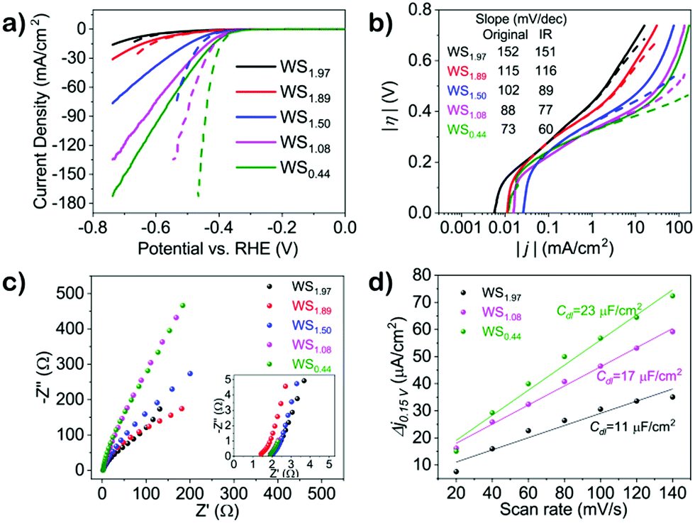
To further demonstrate the applicability of the H2 annealing method to prepare efficient HER catalysts, we have used conductive porous carbon fiber paper (CFP) as substrate. The polarization curves shown in Fig. 7a demonstrate the HER activities of tungsten sulfide with different S/W ratios (XPS shown in Fig. S17, ESI†), which show similar trends for those on SiO2/Si substrates: the smaller the S/W ratio, the higher the HER activity. The linear portions of the Tafel plots before (solid lines, Fig. 7c) and after uncompensated resistance correction (iR-corrected, dashed lines, Fig. 7c) are fitted to the Tafel equation (η = b![[thin space (1/6-em)]](https://www.rsc.org/images/entities/char_2009.gif) logj + a, where j is the current density and b is the Tafel slope), yielding Tafel slopes of ∼73 (without iR correction) or ∼60 mV per decade (iR-corrected). Typically, a Tafel slope of ∼120 mV per decade indicates that the rate-limiting step is the Volmer reaction (H+ + e− → Hads) and the rate-limiting step becomes the Heyrovsky reaction (Hads + H+ + e− → H2) when the Tafel slope is ∼40 mV per decade.22 Therefore, the substantially decreased Tafel slope from 152 mV per decade (WS1.97) to 60 mV per decade (WS0.44) suggests that the HER mechanism on highly defective tungsten sulfide becomes Volmer–Heyrovsky-type with electrochemical desorption of hydrogen as the rate-limiting step.22,43
logj + a, where j is the current density and b is the Tafel slope), yielding Tafel slopes of ∼73 (without iR correction) or ∼60 mV per decade (iR-corrected). Typically, a Tafel slope of ∼120 mV per decade indicates that the rate-limiting step is the Volmer reaction (H+ + e− → Hads) and the rate-limiting step becomes the Heyrovsky reaction (Hads + H+ + e− → H2) when the Tafel slope is ∼40 mV per decade.22 Therefore, the substantially decreased Tafel slope from 152 mV per decade (WS1.97) to 60 mV per decade (WS0.44) suggests that the HER mechanism on highly defective tungsten sulfide becomes Volmer–Heyrovsky-type with electrochemical desorption of hydrogen as the rate-limiting step.22,43
 | ||
| Fig. 7 (a) Linear sweep voltammetry (LSV) curves of WS2−x prepared on carbon fiber paper; dashed lines are obtained after film resistance correction; (b) Tafel slopes for WS2−x obtained from LSV curves in (a); (c) EIS Nyquist plots of corresponding samples collected at open circuit potential with an AC amplitude of 10 mV, inset: zoom-in Nyquist plots; (d) electrochemical double layer capacitance (Cdl) of WS1.97, WS1.08 and WS0.44. Electrolyte: 0.5 M H2SO4, LSV scan rate: 5 mV s−1. | ||
To evaluate the relative differences in electrochemical active surface area of tungsten sulfide with various S/W ratios, we have used cyclic voltammetry (CV). There, we have assumed that the current response recorded in the potential window (0.1–0.2 V vs. RHE) with different scan rates (20–180 mV s−1) (Fig. S19, ESI†) is only due to the capacitive charging of the double layer. By drawing the differences between anodic and cathodic current densities (Δj = ja − jc) against the CV scan rates at a given potential (0.15 V vs. RHE), a linear fitting can be conducted from the curve which is shown in Fig. 7d. The significant increase of active sites for highly defective tungsten sulfide is illustrated by the increase of Cdl from 11 μF cm−2 (WS1.97) to 23 μF cm−2 (WS0.44). Since the significant increase of HER activity far exceeds the increase of surface area, we assume this trend to be related to the intrinsically more active nature of the highly defective tungsten sulfide.
Next to its activity, the stability is a similarly important criterion of a promising electrocatalyst. To evaluate the stability of the as-prepared defective tungsten sulfide, long-duration chronopotentiometric measurements of HER were conducted at a constant current density of 4.45 mA cm−2 for WS0.44, as shown in Fig. S20 (ESI†). There is a slight decrease of the potential at the beginning which quickly stabilizes and remains constant within ±5 mV until the end of the test after 24 h. XPS sputter depth profiling of WS0.44 after HER testing (Fig. S21, ESI†) shows the initial appearance of a sulfate peak and an increase of W(VI)–O peak, which is due to the oxidation of the surface in the electrolyte. However, after 10 cycles (∼20 nm) of Ar+ sputtering, the content of W(VI)–O is similar to fresh samples indicating that oxidation is confined to the topmost surface layers. The highly defective tungsten sulfide film (WS0.44) exhibits a low Tafel slope of 54 mV per decade, which compares well with other reported WS2-based HER catalysts (see Table S1, ESI†).26,44–47
DFT modelling of H adsorption on defective WS2−x
To gain atomic-level insight into the enhanced intrinsic HER activity of W/WS2−x, we have performed DFT calculations to investigate the hydrogen adsorption free energies of the defective tungsten sulfides for HER. Firstly, the Gibbs free energies for hydrogen adsorption (ΔGH) on a stoichiometric WS2(0001) basal plane (BP) (without sulfur vacancies) and defective BP (with S vacancy site) have been calculated, where ΔGH shows a much smaller value of +0.17 eV on an S vacancy site compared to +2.33 eV on the perfect BP (Fig. S22, ESI†). However, the positive value of ΔGH indicates that hydrogen adsorption on both WS2 BP and defective BP is endothermic and therefore unlikely to occur. As discussed, in the H2-annealed material, there co-exist a WS2-rich zone and a W-rich zone where both perfect and defective WS2 BP are present. Even though XPS analysis shows the presence of W–O species on the surface, former studies indicate that W sites in WO3 are inert for hydrogen adsorption.48,49 Also, according to the Pourbaix diagram for the tungsten-water system at 25 °C, the prevailing phase under the applied potential/pH conditions should be W0.50 Therefore, we have calculated ΔGH on a plausible active site model structure in the form of a tetrahedral W4 cluster supported on either perfect (Fig. 8) or defective (Fig. S23, ESI†) basal planes of 2H-WS2. Now, adsorption energies are exothermic and in both cases show a value that is much closer to equilibrium, which indicates that they are HER-active sites. | ||
| Fig. 8 Calculated Gibbs free energy for hydrogen adsorption on the probable adsorption sites of a tetrahedron W cluster on the perfect WS2 basal (0001) plane (BP). | ||
Additionally, we propose that the creation of W-rich zones through the growth of W-clusters on both the perfect and defective WS2 BP may impact on the electronic structure and improve the intrinsic electronic conductivity of the WS2 nanosheets. To verify this hypothesis, we have calculated the partial density of states (PDOS) of the perfect WS2 monolayer and those with a tetrahedral W4 cluster supported on either the perfect or defective basal planes, as shown in Fig. S24 (ESI†). The results indicate that compared to the perfect WS2 monolayer bandgap of 1.98 eV, the growth of the W-clusters on the perfect WS2 monolayer (S/W = 1.72) introduces donor states (intermediate states) in the band gap, whereas W-clusters on the defective WS2 monolayer (S/W = 1.52) narrow the bandgap to 0.85 eV. Through both the intermediate states and the narrowed bandgap, electrons at the valence band edge can be excited more easily to the conduction band edge, suggesting that the growth of W-clusters could introduce more charge carriers and improve the intrinsic conductivity of the WS2 material. The enhanced electrical conductivity together with more optimal hydrogen adsorption energies on the W-clusters are primary reasons leading to the enhanced HER activity of the WS2 materials with lower S/W ratios.
Conclusions
We have presented a versatile method to prepare highly defective tungsten sulfide which exhibits an improved activity in the electrochemical H2 evolution reaction. We have demonstrated the generality of this method by applying it to WS2 supported on various substrates (SiO2/Si, Si3N4, and carbon fiber paper). The S/W ratio, and with that the HER activity, can be tuned via changing the H2 annealing temperature, time and H2 concentration. With decreasing S/W ratio, we succeeded in tuning the amount of S vacancies and W nanoparticles which both are intrinsically more active than the basal planes of WS2. The increased catalytic activity towards hydrogen evolution has been supported by a low Tafel slope of 60 mV per decade for highly defective tungsten sulfide (WS0.44). We presume that the improved HER performance of the highly defective tungsten sulfide films relates to their unique properties which feature the following advantages: (1) nanostructuring and texturization during H2 treatment generate more active sites; (2) the intrinsic catalytic activity of the W clusters on either perfect or defective basal planes contributes to the improvement of activity; (3) the presence of metallic W in the defective WS2−x films improves the intrinsic electronic conductivity thus facilitating charge transfer through the films. Our approach does not only provide a fundamental platform to study the role of sulfur vacancies and W content in highly defective WS2−x in the HER, but it is also applicable to a wide range of other transition metal chalcogenides. To arrive at a conclusive understanding of the role of metallic W species in the HER over-defective WS2−x, further studies, ideally under electrochemical operando conditions, are needed.Conflicts of interest
There are no conflicts to declare.Acknowledgements
This work is part of the program “CO2-neutral fuels” (project 13-CO26) of the Foundation for Fundamental Research on Matter (FOM), which was financially supported by the Netherlands Organization for Scientific Research (NWO). This research program was co-financed by Shell Global Solutions International B.V. Dr Akhil Sharma and Dr Ageeth A. Bol are acknowledged for their assistance in Raman spectra and GI-XRD measurements. Yue Zhang (Eindhoven University of Technology, TU/e) and ESRF beamline staff are acknowledged for their support in μXRD measurements at ESRF during beamtime MA3574. We would like to thank Dr Freddy Oropeza Palacio and Marco Etzi Coller Pascuzzi of TU/e for support in NAP-XPS experiments.References
- B. Seo, G. Y. Jung, Y. J. Sa, H. Y. Jeong, J. Y. Cheon, J. H. Lee, H. Y. Kim, J. C. Kim, H. S. Shin, S. K. Kwak and S. H. Joo, ACS Nano, 2015, 9, 3728–3739 CrossRef CAS PubMed.
- S. S. Chou, N. Sai, P. Lu, E. N. Coker, S. Liu, K. Artyushkova, T. S. Luk, B. Kaehr and C. J. Brinker, Nat. Commun., 2015, 6, 8311–8318 CrossRef CAS PubMed.
- A. A. Tedstone, D. J. Lewis and P. O’Brien, Chem. Mater., 2016, 28, 1965–1974 CrossRef CAS.
- X. Chia, A. Ambrosi, Z. Sofer, J. Luxa and M. Pumera, ACS Nano, 2015, 9, 5164–5179 CrossRef CAS PubMed.
- J. Hu, B. Huang, C. Zhang, Z. Wang, Y. An, D. Zhou, H. Lin, M. K. H. Leung and S. Yang, Energy Environ. Sci., 2017, 10, 593–603 RSC.
- J. D. Benck, Z. Chen, L. Y. Kuritzky, A. J. Forman and T. F. Jaramillo, ACS Catal., 2012, 2, 1916–1923 CrossRef CAS.
- K. Chang, X. Hai, H. Pang, H. Zhang, L. Shi, G. Liu, H. Liu, G. Zhao, M. Li and J. Ye, Adv. Mater., 2016, 28, 10033–10041 CrossRef CAS PubMed.
- F. Wang, J. Li, F. Wang, T. A. Shifa, Z. Cheng, Z. Wang, K. Xu, X. Zhan, Q. Wang, Y. Huang, C. Jiang and J. He, Adv. Funct. Mater., 2015, 25, 6077–6083 CrossRef CAS.
- C. G. Morales-Guio, L.-A. Stern and X. Hu, Chem. Soc. Rev., 2014, 43, 6555–6569 RSC.
- J. K. Norskov, T. Bligaard, J. Rossmeisl and C. H. Christensen, Nat. Chem., 2009, 1, 37–46 CrossRef CAS PubMed.
- Q. Lu, Y. Yu, Q. Ma, B. Chen and H. Zhang, Adv. Mater., 2016, 28, 1917–1933 CrossRef CAS PubMed.
- Z. W. Seh, J. Kibsgaard, C. F. Dickens, I. Chorkendorff, J. K. Norskov and T. F. Jaramillo, Science, 2017, 355, eaad4998 CrossRef PubMed.
- J. Kibsgaard, Z. Chen, B. N. Reinecke and T. F. Jaramillo, Nat. Mater., 2012, 11, 963–969 CrossRef CAS PubMed.
- X. Zhao, X. Ma, J. Sun, D. Li and X. Yang, ACS Nano, 2016, 10, 2159–2166 CrossRef CAS PubMed.
- H. Li, C. Tsai, A. L. Koh, L. Cai, A. W. Contryman, A. H. Fragapane, J. Zhao, H. S. Han, H. C. Manoharan, F. Abild-Pedersen, J. K. Nørskov and X. Zheng, Nat. Mater., 2015, 15, 48–53 CrossRef PubMed.
- G. Ye, Y. Gong, J. Lin, B. Li, Y. He, S. T. Pantelides, W. Zhou, R. Vajtai and P. M. Ajayan, Nano Lett., 2016, 16, 1097–1103 CrossRef CAS PubMed.
- T. F. Jaramillo, K. P. Jørgensen, J. Bonde, J. H. Nielsen, S. Horch and I. Chorkendorff, Science, 2007, 317, 100–102 CrossRef CAS PubMed.
- H. Wang, H. Yuan, S. S. Hong, Y. Li and Y. Cui, Chem. Soc. Rev., 2015, 44, 2664–2680 RSC.
- Y.-R. An, X.-L. Fan, Z.-F. Luo and W.-M. Lau, Nano Lett., 2016, 17, 368–376 CrossRef PubMed.
- Y. Yang, H. Fei, G. Ruan, Y. Li and J. M. Tour, Adv. Funct. Mater., 2015, 25, 6199–6204 CrossRef CAS.
- C. Tsai, H. Li, S. Park, J. Park, H. S. Han, J. K. Norskov, X. Zheng and F. Abild-Pedersen, Nat. Commun., 2017, 8, 15113 CrossRef PubMed.
- C.-C. Cheng, A.-Y. Lu, C.-C. Tseng, X. Yang, M. N. Hedhili, M.-C. Chen, K.-H. Wei and L.-J. Li, Nano Energy, 2016, 30, 846–852 CrossRef CAS.
- J. M. Woods, Y. Jung, Y. Xie, W. Liu, Y. Liu, H. Wang and J. J. Cha, ACS Nano, 2016, 10, 2004–2009 CrossRef CAS PubMed.
- H. Wang, Z. Lu, S. Xu, D. Kong, J. J. Cha, G. Zheng, P. C. Hsu, K. Yan, D. Bradshaw, F. B. Prinz and Y. Cui, Proc. Natl. Acad. Sci. U. S. A., 2013, 110, 19701–19706 CrossRef CAS PubMed.
- D. Kiriya, P. Lobaccaro, H. Y. Nyein, P. Taheri, M. Hettick, H. Shiraki, C. M. Sutter-Fella, P. Zhao, W. Gao, R. Maboudian, J. W. Ager and A. Javey, Nano Lett., 2016, 16, 4047–4053 CrossRef CAS PubMed.
- Z. Wu, B. Fang, A. Bonakdarpour, A. Sun, D. P. Wilkinson and D. Wang, Appl. Catal., B, 2012, 125, 59–66 CrossRef CAS.
- L. Wu, N. Y. Dzade, L. Gao, D. O. Scanlon, Z. Ozturk, N. Hollingsworth, B. M. Weckhuysen, E. J. Hensen, N. H. de Leeuw and J. P. Hofmann, Adv. Mater., 2016, 28, 9602–9607 CrossRef CAS PubMed.
- G. J. A. Mannie, J. van Deelen, J. W. Niemantsverdriet and P. C. Thüne, Appl. Phys. Lett., 2011, 98, 051907 CrossRef.
- G. J. A. Mannie, J. van Deelen, J. W. Niemantsverdriet and P. C. Thüne, Appl. Surf. Sci., 2014, 309, 263–270 CrossRef CAS.
- E. Erasmus, P. C. Thüne, M. W. G. M. Verhoeven, J. W. Niemantsverdriet and J. C. Swarts, Catal. Commun., 2012, 27, 193–199 CrossRef CAS.
- P. C. Thüne, C. J. Weststrate, P. Moodley, A. M. Saib, J. van de Loosdrecht, J. T. Millerc and J. W. Niemantsverdrieta, Catal. Sci. Technol., 2011, 1, 689–697 RSC.
- Y. Jung, J. Shen, Y. Liu, J. M. Woods, Y. Sun and J. J. Cha, Nano Lett., 2014, 14, 6842–6849 CrossRef CAS PubMed.
- T. A. Loh, D. H. Chua and A. T. Wee, Sci. Rep., 2015, 5, 18116 CrossRef CAS PubMed.
- L. Ma, J. Peng, C. Wu, L. He and Y. Ni, ACS Nano, 2017, 11, 2928–2933 CrossRef CAS PubMed.
- Y. D. Li, X. L. Li, R. R. He, J. Zhu and Z. X. Deng, J. Am. Chem. Soc., 2002, 124, 1411–1416 CrossRef CAS PubMed.
- S. M. Ng, H. F. Wong, W. C. Wong, C. K. Tan, S. Y. Choi, C. L. Mak, G. J. Li, Q. C. Dong and C. W. Leung, Mater. Chem. Phys., 2016, 181, 352–358 CrossRef CAS.
- L. Ma, Y. Hu, G. Zhu, R. Chen, T. Chen, H. Lu, Y. Wang, J. Liang, H. Liu, C. Yan, Z. Tie, Z. Jin and J. Liu, Chem. Mater., 2016, 28, 5733–5742 CrossRef CAS.
- F. Wang, P. He, Y. Li, T. A. Shifa, Y. Deng, K. Liu, Q. Wang, F. Wang, Y. Wen, Z. Wang, X. Zhan, L. Sun and J. He, Adv. Funct. Mater., 2017, 27, 1605802 CrossRef.
- M. A. Pimenta, E. Del Corro, B. R. Carvalho, C. Fantini and L. M. Malard, Acc. Chem. Res., 2015, 48, 41–47 CrossRef CAS PubMed.
- A. Berkdemir, H. R. Gutiérrez, A. R. Botello-Méndez, N. Perea-López, A. L. Elías, C.-I. Chia, B. Wang, V. H. Crespi, F. López-Urías, J.-C. Charlier, H. Terrones and M. Terrones, Sci. Rep., 2013, 3, 1755 CrossRef.
- A. Molina-Sánchez and L. Wirtz, Phys. Rev. B: Condens. Matter Mater. Phys., 2011, 84, 155413 CrossRef.
- A. P. S. Gaur, S. Sahoo, M. Ahmadi, M. J. F. Guinel, S. K. Gupta, R. Pandey, S. K. Dey and R. S. Katiyar, J. Phys. Chem. C, 2013, 117, 26262–26268 CrossRef CAS.
- Y. Li, H. Wang, L. Xie, Y. Liang, G. Hong and H. Dai, J. Am. Chem. Soc., 2011, 133, 7296–7299 CrossRef CAS PubMed.
- D. Voiry, H. Yamaguchi, J. Li, R. Silva, D. C. B. Alves, T. Fujita, M. Chen, T. Asefa, V. B. Shenoy, G. Eda and M. Chhowalla, Nat. Mater., 2013, 12, 850–855 CrossRef CAS PubMed.
- J. Yang, D. Voiry, S. J. Ahn, D. Kang, A. Y. Kim, M. Chhowalla and H. S. Shin, Angew. Chem., Int. Ed., 2013, 52, 13751–13754 CrossRef CAS PubMed.
- L. Cheng, W. Huang, Q. Gong, C. Liu, Z. Liu, Y. Li and H. Dai, Angew. Chem., Int. Ed., 2014, 53, 7860–7863 CrossRef CAS PubMed.
- J. Duan, S. Chen, B. A. Chambers, G. G. Andersson and S. Z. Qiao, Adv. Mater., 2015, 27, 4234–4241 CrossRef CAS PubMed.
- F. Wang, C. Di Valentin and G. Pacchioni, J. Phys. Chem. C, 2012, 116, 10672–10679 CrossRef CAS.
- T. Zheng, W. Sang, Z. He, Q. Wei, B. Chen, H. Li, C. Cao, R. Huang, X. Yan, B. Pan, S. Zhou and J. Zeng, Nano Lett., 2017, 17, 7968–7973 CrossRef CAS PubMed.
- S. Bothra, H. Sur and V. Liang, Microelectron. Reliab., 1999, 39, 59–68 CrossRef.
Footnote |
| † Electronic supplementary information (ESI) available: Experimental details and additional characterization. See DOI: 10.1039/c9cp00722a |
| This journal is © the Owner Societies 2019 |