
 Open Access Article
 This Open Access Article is licensed under a Creative Commons Attribution-Non Commercial 3.0 Unported Licence
Nanoplatelet cryoaerogels with potential application in photoelectrochemical sensing†
Anja
Schlosser
ab,
Lea C.
Meyer
ab,
Franziska
Lübkemann
ab,
Jan F.
Miethe
ab and
Nadja C.
Bigall
 *ab
*ab
aInstitute of Physical Chemistry and Electrochemistry, Leibniz Universität Hannover, Callinstr. 3A, 30167 Hannover, Germany. E-mail: nadja.bigall@pci.uni-hannover.de; Fax: +49 511 762 19121; Tel: +49 511 762 3185
bLaboratory of Nano and Quantum Engineering (LNQE), Leibniz Universität Hannover, Schneiderberg 39, 30167 Hannover, Germany
First published on 6th March 2019
Abstract
Semiconductor nanoparticle based porous 3D assemblies are interesting materials for various applications in the fields of photovoltaics, catalysis, or optical sensing. For use as photoelectrodes in photoelectrochemical sensors they need to be characterised by a high porosity, a good photostability, and a high charge carrier mobility. Our work reports on the preparation of cryoaerogel photoelectrodes based on CdSe nanoplatelets and their photoelectrochemical characterisation by means of linear sweep voltammetry (LSV) and intensity modulated photocurrent spectroscopy (IMPS). The obtained open-pored cryoaerogel films were observed to produce much higher photocurrents than comparable drop-cast films. By means of IMPS, the performance differences could be linked to the occurrence of charge carrier movement, which could solely be proven for the cryoaerogels. In a proof-of-principle experiment, the potential of the prepared photoelectrodes for application in photoelectrochemical sensing was moreover demonstrated.
Introduction
Photoelectrochemical sensors based on semiconductor nanoparticles (NPs) have been intensively researched in recent decades, as they exhibit high sensitivities, fast responses, and a broad analyte range.1–3 One particular advantage of this sensor type is the independence of the excitation signal (light) and the detection signal (current), which does not only yield low detection limits but could also enable the detection of multiple analytes by one and the same probe.1,4 To date, numerous types of semiconductor NP sensitised photoelectrodes for sensing applications have already been developed, including self-assembled NP monolayers,5–9 and layer-by-layer,10–14 and cross-linked15,16 assemblies. Multilayered systems in general were shown to exhibit distinctly higher photocurrents than comparable monolayer systems, with the photocurrent being observed to scale with the number of layers deposited.13–16 However, in order to avoid charging of the NPs and to mediate the electron transfer between the particles within the assembly, incorporation of redox-active species into the multilayers was often required.13,15 Although the application of these species leads to enhanced photocurrents, they may interfere with analyte molecules if the photoelectrodes are to be applied as photoelectrochemical sensors.1,17 Therefore it is desirable to avoid the use of redox-active species in the construction of photoelectrodes while preserving the high charge carrier transfer rates between the particles.As one alternative to the afore-mentioned NP assemblies, porous self-supporting NP (aero)gels could be considered. (Aero)gels are characterised by a high porosity and large surface areas (and, due to their hierarchical porosity, by good accessibility of the surface), as well as particle–particle contacts which enable charge carrier mobility.18–21 Semiconductor NP based gels can be formed from colloidal NP solutions e.g. by the addition of chemical reagents which are able to remove the stabilising ligands from the NP surface18–20,22 or to serve as cross-linkers,23,24 or by physical methods.21,25 Through the use of mild gelation conditions it is possible to assemble NPs in such a way that their nanoscopic properties are partially retained even though they are in direct contact with each other. The direct particle–particle contacts were observed to facilitate the charge carrier delocalisation and transport within the structures, leading to prolonged fluorescence lifetimes as well as enhanced photoelectrochemical performance.19,26,27 In this work, we report on the fabrication and photoelectrochemical characterisation of cryoaerogel coated photoelectrodes which can be applied as photolectrochemical sensors. The prepared cryoaerogels are based on quasi-rectangular CdSe nanoplatelets (NPLs) with a thickness of 4 monolayers (MLs), which should show excellent electrochemical properties due to their very high surface-to-volume ratio. However, CdSe NPLs could so far only be assembled into stable 3D structures by time-consuming chemical gelation or by polymer encapsulation.20,28 By application of the comparably mild cryoaerogelation method, it was possible to assemble NPLs into open and porous structures consisting of stacked sheets (Fig. 1) without them being altered. The thickness and morphology of the obtained structures could easily be modified by the variation of different manufacturing parameters, such as the particle concentration and amount. The cryoaerogel morphology was observed to strongly influence the charge carrier transport within the structures and therefore their photoelectrochemical performance, which was proven by means of intensity modulated photocurrent spectroscopy (IMPS). Until now, IMPS was mainly employed in the characterisation of materials for solar or photoelectrochemical cells,29–32 as well as nanoparticle monolayers.9,33,34 We have recently demonstrated that IMPS can also be a useful method to gain insights into the charge carrier dynamics in nanoparticle assemblies.27,28 The IMPS investigations on cryoaerogels, as shown in the present work, revealed that charge carriers are able to move through the NPL network, which leads to a significant enhancement of the photocurrent. To moreover demonstrate the applicability of the cryoaerogel coated photoelectrodes for photoelectrochemical sensing, we finally conducted a proof-of-principle experiment comprising the measurement of the photoresponse to ferricyanide ions.
 | ||
| Fig. 1 Schematic drawing of the cryoaerogel photoelectrode preparation process. After the synthesis in organic solvents (1), the NPLs were transferred to an aqueous phase by ligand exchange (2). Afterwards, the concentrated aqueous NPL solutions were dropped onto functionalised tin doped indium oxide (ITO) coated glass electrodes (3) and flash-frozen in liquid nitrogen (4). Finally, the ice crystals which were formed during the freezing process were removed by lyophilisation (5) to yield highly porous cryoaerogel films on the electrode surface. | ||
Experimental
Chemicals
Cadmium nitrate tetrahydrate (Cd(NO3)2·4H2O, >98%), sodium myristate (Na(myr), >99%), 1-octadecene (ODE, 90%), cadmium acetate dihydrate (Cd(OAc)2·2H2O, >98%), oleic acid (OLA, >90%), n-hexane (≥99%), 11-mercaptoundecanoic acid (MUA, 95%), acetone (99.5%), potassium hydroxide (KOH, >85%), ammonium hydroxide (NH4OH, 28–30%), hydrogen peroxide (H2O2, 30%), toluene (99.7%), (3-mercaptopropyl)trimethoxysilane (MPTMS, 95%), sulfuric acid (H2SO4) (95–97%), potassium ferricyanide(III) trihydrate (≥98.5%), sodium dihydrogen phosphate dihydrate (99%), and disodium hydrogen phosphate dodecahydrate (99%) were purchased from Sigma-Aldrich. Methanol (MeOH, ≥99.8%), 2-propanol (99.5%), and ethanol (EtOH, ≥99.8%) were purchased from Roth. Selenium (200 mesh, 99.999%) was purchased from Alfa Aesar. Sodium sulfite (Na2SO3) (>97%) was purchased from Fisher Scientific. All chemicals were used as received without further purification.Synthesis procedures
Photoelectrode preparation
![[thin space (1/6-em)]](https://www.rsc.org/images/entities/char_2009.gif) :1:1 v/v% H2O:NH3:H2O2 solution (2 h at 50 °C). Afterwards, the cleaned electrodes were carefully rinsed with water, isopropanol, and toluene. Following this, the electrodes were functionalised in a solution containing 1 v/v% of MPTMS in toluene (2 h at 50 °C). Finally, the electrodes were removed from the functionalisation solution and excess MPTMS was rinsed off with toluene.
:1:1 v/v% H2O:NH3:H2O2 solution (2 h at 50 °C). Afterwards, the cleaned electrodes were carefully rinsed with water, isopropanol, and toluene. Following this, the electrodes were functionalised in a solution containing 1 v/v% of MPTMS in toluene (2 h at 50 °C). Finally, the electrodes were removed from the functionalisation solution and excess MPTMS was rinsed off with toluene.
Characterisation methods
Linear sweep voltammograms were recorded in a 0.5 M Na2SO3 buffer solution at different pH values between 9 and 6. The solution pH was adjusted with H2SO4 and measured with a calibrated pH probe. During the LSV measurement, the bias potential was swept from −600 mV to 300 mV versus Ag/AgCl with a sweep velocity of 4 mVs−1.
Intensity modulated photocurrent spectra were recorded in a 0.5 M Na2SO3 buffer solution at pH 7. Unless otherwise stated, the experiments were performed at a bias potential of 300 mV versus Ag/AgCl with applied iR-drop compensation of the potentiostat. The photon flux was modulated with a sine wave function in the frequency range between 10 kHz and 1 Hz. The frequency dependent photon flux of the LED was determined by a Si photodiode (Fig. S36, ESI†).
Chronoamperograms were measured to demonstrate the applicability of the fabricated electrodes for photoelectrochemical sensing. All measurements were carried out in a 0.1 M HPO42/H2PO4− buffer at pH 8. Prior to increasing the analyte concentration in the electrolyte, all electrodes were immersed for one hour in the phosphate buffer solution. Then, a 10 mM solution of K3[Fe(CN)6] dissolved in phosphate buffer was added progressively. The bias potential was kept constant at −450 mV versus Ag/AgCl.
Results and discussion
Fabrication and morphological characterisation of NPL cryoaerogel photoelectrodes
CdSe NPLs with a thickness of approximately 1.2 nm, corresponding to 4 monolayers (MLs), were synthesised according to a previously published procedure.36 A TEM micrograph of the as-synthesised sample in hexane (Fig. 2A) reveals that NPLs with a quasi-rectangular morphology and edge lengths of 22.8 nm ± 2.9 nm × 7.1 nm ± 1.4 nm were obtained. The full optical characterisation of the pristine NPLs is presented in the ESI† (Fig. S3). During the cryaerogelation process, the density anomaly of water is utilised to form porous aerogels out of highly concentrated nanoparticle solutions.21,38 Therefore, a phase transfer of the NPLs from hexane to an aqueous phase was necessary. Water soluble NPLs were synthesised by exchanging the native oleic acid ligands against bi-functional MUA ligands.37 The thiol group of the MUA ligand binds strongly to the surface of the NPLs, whereas the carboxyl group enables the water solubility at neutral to basic pH-values. Due to the ligand exchange with MUA, a bathochromic shift and a weakening of the excitonic absorption features of the NPLs are observed, as can been seen in the UV/vis spectra (Fig. 2B).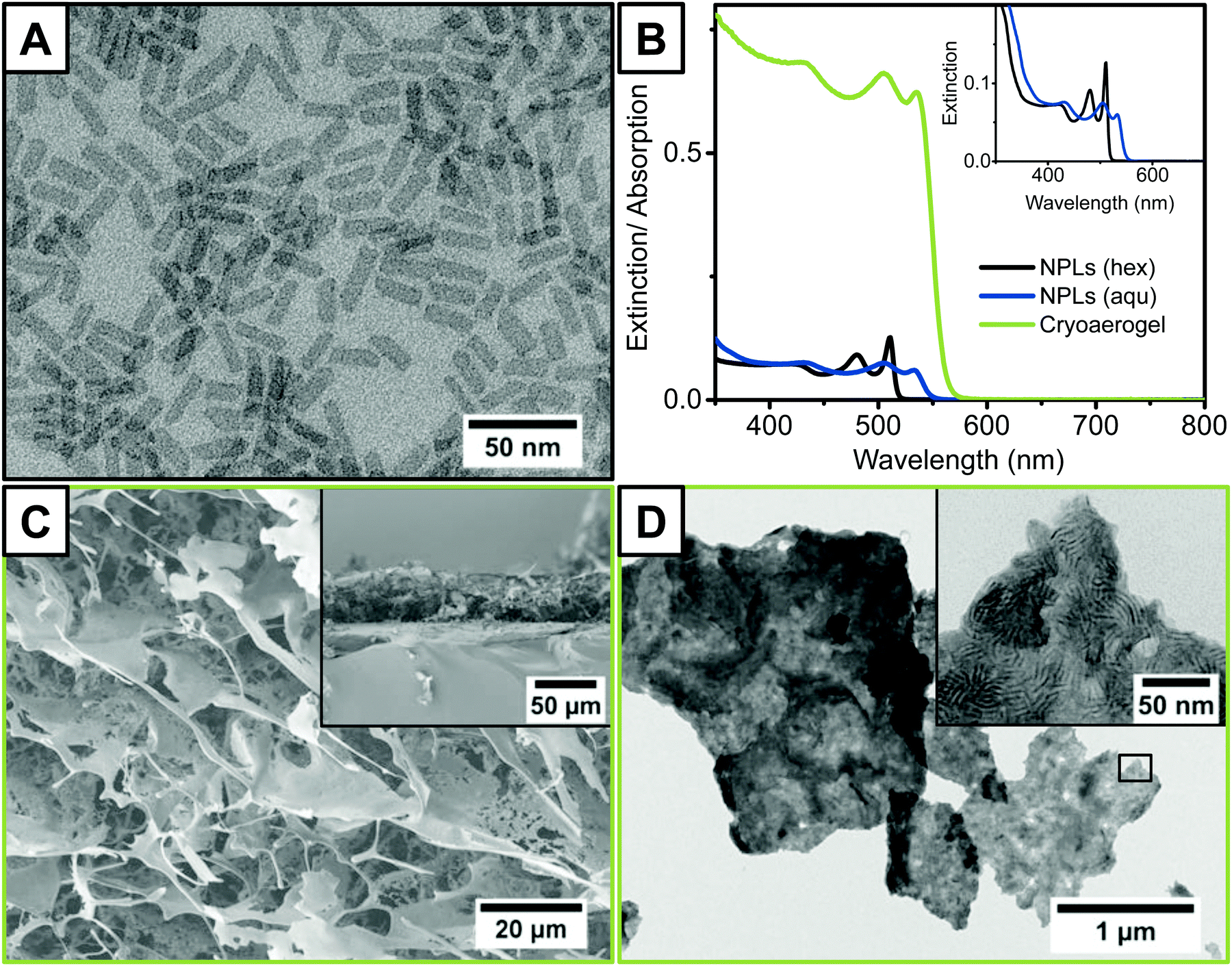 | ||
| Fig. 2 Morphological and optical characterisation of the NPL building blocks (A and B) and the cryoaerogel films (B–D). (A) TEM micrograph of as-synthesised CdSe NPLs with a thickness of 4 MLs. (B) Extinction spectra of as-synthesised CdSe NPLs (grey) and phase-transferred CdSe NPLs (blue) measured at the same Cd concentration of 41 µM, and the absorption spectrum of a NPL cryoaerogel film on an ITO coated glass electrode (20 µL cm−2, 28 mM Cd concentration, 1 × 10⁻² M KOH). The inset shows a magnification of the OD region between 0 and 0.2 for a better comparison of the NPL spectra. Normalised spectra of all three samples can be found in the ESI† (Fig. S5). (C and D) SEM (C) and TEM (D) micrographs of the respective NPL cryoaerogel in different magnifications. The inset in (C) shows the cross-section of a CdSe NPL cryoaerogel film on an ITO-coated glass electrode. | ||
Subsequently, the aqueous NPL solution was dropped into a mold created out of adhesive tape on functionalised ITO glass. The electrode was then dipped rapidly into liquid nitrogen to shock-freeze the NPL solution and to create a large number of small ice crystallites. Finally, the ice was removed by lyophilisation. To ensure the formation of stable cryoaerogel thin films, the ligand concentration in the employed nanoparticle solution needs to be sufficiently low.21 If the ligand concentration is too high, sheet-like structures typical for cryoaerogels are still formed (Fig. S23, ESI†), but they are only weakly attached to the glass electrode surface. The electrode surface was functionalised with MPTMS prior to cryoaerogelation to improve the wettability of the surface and to facilitate the (electrical) interconnection between the NPLs and the electrode. However, if the concentration of free ligands in the applied NPL solution is much higher than the MPTMS concentration on the electrode surface, no driving force for the adsorption of the NPLs onto the electrode surface is present. The reduction of the concentration of the free ligands in the NPL solution was achieved by introducing a washing step prior to re-dispersion of the NPLs in the respective aqueous KOH solution. In this way, cryoaerogel films sufficiently attached to the ITO glass surface could be obtained (Fig. 2C, inset). The scanning electron microscopy (SEM) image of the film surface (Fig. 2C) illustrates the morphology of the CdSe NPL cryoaerogel films. The observed structure consisting of interconnected sheet-like assemblies which are partially scrolled to wires is comparable to previous reports on cryoaerogels based on other nanoparticle materials.21,38,39 Due to the directed stacking of the sheets, macroporous assemblies are obtained, as can be derived from the Kr physisorption measurements (Fig. S24, ESI†). The sheets themselves exhibit a filigree fine-structure with lots of holes. In the transmission electron microscopy (TEM) image (Fig. 2D), some single cryoaerogel sheets are visible. The higher magnification TEM image (Fig. 2D, inset) reveals that the sheets consist of stacked and folded NPLs, which are in close proximity to each other. Stacked NPLs perpendicular to the TEM grid appear as dark stripes whereas NPLs parallel to the TEM grid appear in a lighter grey, due to the differences in the TEM contrast. The NPL building blocks therefore seem to remain unaltered in the cryoaerogel formation process. The preservation of the crystal structure and the crystallite size was moreover confirmed by XRD (Fig. S11, ESI†). The positions of the main reflections of the cryoaerogel sample are only negligibly shifted towards higher 2θ compared to the aqueous NPL building blocks. In the UV/vis absorption spectrum of the cryoaerogel films (Fig. 2B), the typical sharp absorption features of CdSe NPLs are still present and only slightly shifted towards longer wavelengths by 2 nm (9 meV) compared to the aqueous NPL solution. This again confirms the retention of the nanocrystallinity and therefore the quantum confinement in the solid.18–20 Moreover it can be derived that no remarkable changes in the NPL thickness due to the cryoaerogelation have occurred. If etching of the NPL building blocks were to take place, a strong hypsochromic shift of the absorption edge would be expected, as was observed for a chemically fabricated CdSe NPL aerogel.20 The slight bathochromic shift of the absorption maximum and the absorption onset, however, could originate either from enhanced electronic coupling due to much lower inter-particle distances or from growth of the crystallites.26,40 We moreover examined the homogeneity of the produced cryoaerogel coatings by UV/vis absorption spectroscopy and SEM. The results are presented in the ESI† (Fig. S12–S14).
In order to investigate the factors determining the cryoaerogel structure, we varied a range of parameters, such as the film thickness, the NPL concentration, and the KOH concentration. The film thickness can be easily influenced by varying the volume of the applied NPL solution. The lowest solution amount that can be uniformly distributed in the 1 cm2 mold is 10 µL. If no shrinkage during the cryoaerogelation process occurs, the resulting film thickness would be 106 µm. However, SEM images of the film cross-section (Fig. S15, ESI†) reveal a shrinkage of around 57%, so that a continuous film with an approximate thickness of 45.8 µm ± 6.2 µm was obtained. The film thickness can be increased to 120. 5 µm ± 12.9 µm, if 40 µL cm−2 of the NPL solution is applied. A further increase of the solution volume leads to inhomogeneous films, which often partially detach from the substrate. The morphology of the films, however, can be influenced by varying the NPL concentration or the KOH concentration. By a variation of the NPL concentration, the thickness and density of the sheet-like assemblies on the substrate surface can be changed. Fig. 3 shows SEM images of cryoaerogels obtained from differently concentrated NPL solutions. In the case of low NPL concentrations, the electrode surface is only partially covered by the cryoaerogel sheets (Fig. 3A left). The sheets are moreover randomly oriented and possess a rough surface, probably due to the formation of pure KOH crystallites within the sheets. If a NPL solution with a Cd concentration of 28 mM is applied (Fig. 3B), the whole substrate is covered by randomly oriented sheets with a slightly smoother surface, but lots of holes. A further increase of the NPL concentration leads to partially ordered assemblies of sheets on the substrate surface (Fig. 3C). The sheets themselves are observed to be much smoother and thicker than in the case of lower NPL concentrations. As a last parameter, the concentration of aqueous KOH, which was used for the re-dispersion of the phase transferred NPLs, was varied. The KOH concentration was observed to mainly influence the morphology of the fabricated cryoaerogels. SEM investigations (Fig. S22, ESI†) show that the typical cryoaerogel morphology is only obtained for KOH concentrations of less or equal than 1 × 10⁻² M. For higher KOH concentrations, dense and rather inhomogeneous particle layers are formed on the substrate (Fig. S22 left, ESI†). Within the dense coatings, large crystallites are visible, probably consisting of pure KOH. The completely different morphology of the obtained cryoaerogels could be attributed to the high amount of KOH, which might be able to disturb the formation of small ice crystals during the fast-freezing process. The morphological differences of cryoaerogels fabricated from lower concentrations of KOH (1 × 10⁻² M, 1 × 10⁻³ M, 1 × 10⁻⁵ M, or 0 M) are much smaller and can be most easily identified in the TEM images (Fig. S23, ESI†). The TEM contrast of the sheets decreases with the KOH concentration, thus the KOH concentration mainly affects the sheet thickness in this concentration regime, so that the thinnest sheets are consequently formed at the lowest KOH concentration.
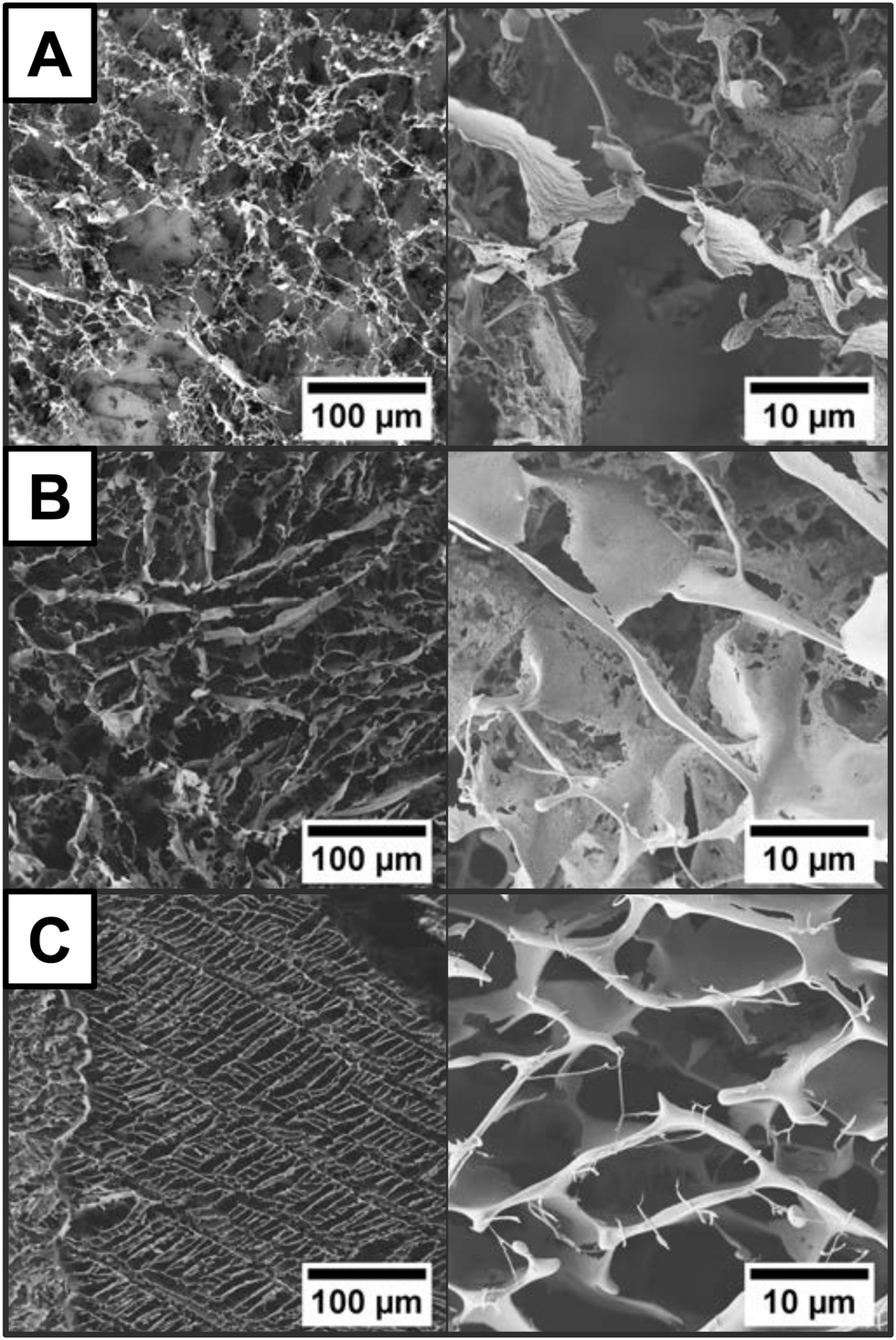 | ||
| Fig. 3 SEM images of different CdSe NPL cryoaerogel coatings. The concentration of Cd2+ in the original aqueous NPL solutions increases from panel A to C (A: 10 mM, B: 28 mM, and C: 70 mM). For the preparation of each sample, 20 µL of the respective NPL solution was used. The KOH concentration was kept constant at 1 × 10⁻² M. | ||
Photoelectrochemical characterisation of NPL cryoaerogel photoelectrodes
The obtained cryoaerogel-coated photoelectrodes were photoelectrochemically characterised by means of linear sweep voltammetry (LSV) and intensity modulated photocurrent spectroscopy (IMPS). All measurements were carried out in a self-built measurement cell34 using a three electrode setup comprising the NPL-coated electrode as the working electrode, a roughened Pt wire as the counter electrode, and a Ag/AgCl (3 M NaCl) reference electrode. As the electrolyte, a SO32−/HSO3− buffer at a concentration of 0.5 M was applied. Sodium sulfite acts as a hole scavenger and was already shown to effectively prevent photocorrosion of various cadmium chalcogenide NPs.28,34,41,42LSVs were recorded in a bias potential range between −600 mV and 300 mV (versus Ag/AgCl), in which CdSe NPLs should be neither oxidised nor reduced (Fig. S25, ESI†).43 The photoelectrodes were periodically illuminated with a 468 nm LED light source to evaluate the bias-dependent photoresponse of the prepared cryoaerogel films. Fig. 4A shows the LSVs of a CdSe NPL cryoaerogel film in comparison to LSVs of a CdSe NPL (sub-)monolayer and a CdSe NPL multilayer electrode. The preparation of the latter two photoelectrode types is described in the Experimental section. For all three electrode types, only positive photocurrents, which are related to sulfite oxidation (green arrows in Fig. S25, ESI†),9,34 are observed in the whole potential range. If the electrolyte pH is increased, however, also negative photocurrents can be recorded at negative bias potentials (Fig. S26, ESI†). The (sub-)monolayer electrodes show very low photocurrents in the nA-range, which may be explained by the sparse particle coverage of the electrode confirmed by the low absorption (Fig. S21, ESI†). An increase of the electrode surface coverage and light absorption by either applying multilayer or cryoaerogel coatings leads to orders of magnitude larger photocurrents. However, although the NPL amount deposited on the electrode was similar in both cases (multilayer and cryoaerogel), cryoaerogel photoelectrodes show enhanced photocurrent generation compared to their multilayer counterparts. This observation could be attributed to photocurrent contributions of NPLs, which are not directly connected to the electrode surface but part of the cryoaerogel network. Due to their open and porous structure, CdSe NPL cryoaerogels can be penetrated more quickly by the electrolyte than the corresponding dense multilayers. In addition, low interparticle distances of the NPLs within the sheets were observed for the NPL cryoaerogels (Fig. 2C and D), so that movement of charge carriers between particles should be possible. In the particle multilayers, in contrast, the interparticle distances are expected to be greater than or equal to the length of the MUA ligands.44
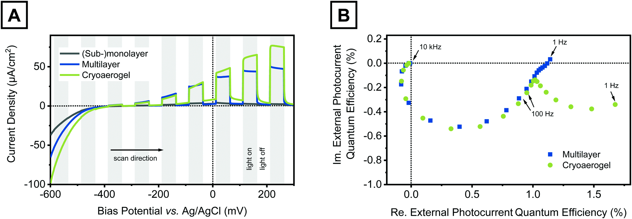 | ||
| Fig. 4 Photoelectrochemical characterisation results of different photoelectrodes coated with CdSe NPLs at pH 7. For the multilayer and cryoaerogel preparation, 20 µL of an aqueous NPL solution (28 mM) dispersed in 1 × 10⁻³ M KOH was used. (A) LSVs of a CdSe NPL (sub-)monolayer (grey), a multilayer (blue), and a cryoaerogel (green) coated photoelectrode recorded under alternating irradiation with a blue LED. (B) IMPS spectra of a multilayer (blue squares) and a cryoaerogel (green circles) coated photoelectrode recorded at a bias potential of 300 mV. | ||
We further investigated the charge carrier transport in both NPL assemblies by IMPS. Over the course of the IMPS experiments, the on–off frequency of the LED is varied (in our case from 10 kHz to 1 Hz) and the photocurrent response of the investigated system is recorded.45 In this way it is possible to distinguish between charge transfer processes occurring on different timescales, as long as their rate constants differ by at least one order of magnitude.34 The IMPS responses of the multilayer and the cryoaerogel coated electrodes are displayed in Fig. 4B. In the Nyquist complex plane plots, nearly perfect semicircles are observed in the frequency range between 10 kHz and 25 Hz for both photoelectrode types. These semicircles are related to the two charge transfer processes that are involved in the generation of positive photocurrents (green arrows in Fig. S25, ESI†). The crossover from the third to the fourth quadrant at high frequencies shows that the electron injection into the substrate is slightly delayed with respect to the hole transfer to sulfite.9 In the lower frequency range, a second semicircle adjacent to the first one is observed for the cryoaerogel coated photoelectrode. This semicircle cannot be related to the afore-mentioned charge transfer processes involving solely the first particle monolayer. We attribute this second semicircle to bias-potential driven charge carrier transport across the illuminated NPL assemblies.32,33,45 In the relevant frequency range, this process competes with the surface recombination of trapped charge carriers and back-electron transfer processes.9,29,30 However, the presence of these loss mechanisms would be reflected in a return of the IMPS response to the real axis or even a crossover into the first quadrant (photocurrent leads the light) combined with no further increase or even a decrease of the photocurrent.9,29,30,45 A comparable behaviour is only observed for the multilayer electrodes, so that the afore-mentioned loss mechanisms gain increased relevance for this assembly type, whereas for the cryoaerogel photoelectrodes the charge carrier diffusion seems to be the clearly dominating process in the low frequency regime. However, the comparison of the LSVs of both electrodes suggests not only the existence of inter-particle charge carrier movement but also its bias-potential dependence, as the photocurrent difference between both electrodes increases with increasing bias potential. To further corroborate this presumption, additional IMPS spectra of the cryoaerogel electrode were recorded at 0 and 150 mV bias potentials (Fig. S27, ESI†). These show that the ratio of the low frequency semicircle to the high frequency semicircle increases with the bias potential, hence the contribution of the charge carrier diffusion to the photocurrent increases likewise. For all three bias potentials it was moreover observed that the measured IMPS response does not return to the real axis (no phase lag of the photocurrent related to the photon flux), even at the lowest applied frequency of 1 Hz. This suggests that the investigated system has not reached its steady-state at that point,28,32 which is also reflected in the steady increase of the photocurrent during the illumination period (Fig. 4A, green curve).
The morphology of the cryoaerogel coatings was already shown to be strongly dependent on various manufacturing parameters. It is expected that the morphological differences will also be reflected in the photoelectrochemical performance. The film thickness mainly influences the amount of generated photocurrent, as can be seen from the LSVs (Fig. S28, ESI†). The photocurrent increases with increasing film thickness, however, no linear relation between both is observed. This implies that the efficiency of photoelectrodes with thinner films is remarkably higher than the efficiency of thicker film photoelectrodes. This observation could be explained by two synergistic effects. At first, the illumination intensity will be higher for particles close to the substrate compared to particles far away from the substrate, as the samples are typically illuminated from the substrate side only and as they are not optically thin. Furthermore, the IMPS response of the cryoaerogel electrode (Fig. 4B) already revealed that the photocurrent contribution of the particles directly attached to the substrate is slightly larger than the contribution of all other particles in total, as the charge carrier extraction from the outer layers is less effective due to the potential gradient and the occurrence of charge carrier recombination at the particle boundaries.
Fig. 5 shows the IMPS responses of cryoaerogel films with different thicknesses. The IMPS responses were recorded under backside and frontside illumination, respectively, at a bias potential of 300 mV. In all IMPS plots, two semicircles adjacent to each other were observed. Under backside illumination (Fig. 5A), the radius of the high frequency semicircle was observed to increase with increasing solution volume. However, the difference between the 10 µL sample (lowest thickness) and the 20 µL sample (medium thickness) is relatively small. This can be attributed to the fact that the density of particles directly attached to the electrode surface is similar for both electrodes, as in this specific case a nearly linear increase of the film thickness with the applied solution volume was observed (10 µL: 45.8 µm, 20 µL: 87.1 µm, derived from SEM cross-section measurements). For higher solution volumes, in contrast, a greater shrinkage of the cryoaerogels during the drying process occurred, so that the linear relation between the film thickness and solution volume is not longer valid (thickness of the 40 µL sample: 120.5 µm). This however leads to the formation of higher density cryoaerogels if large solution volumes (>20 µL) are applied, and a therefore larger particle amount at the interface with the substrate. The measured IMPS response for the 40 µL sample is in line with this observation (a larger high frequency semicircle).
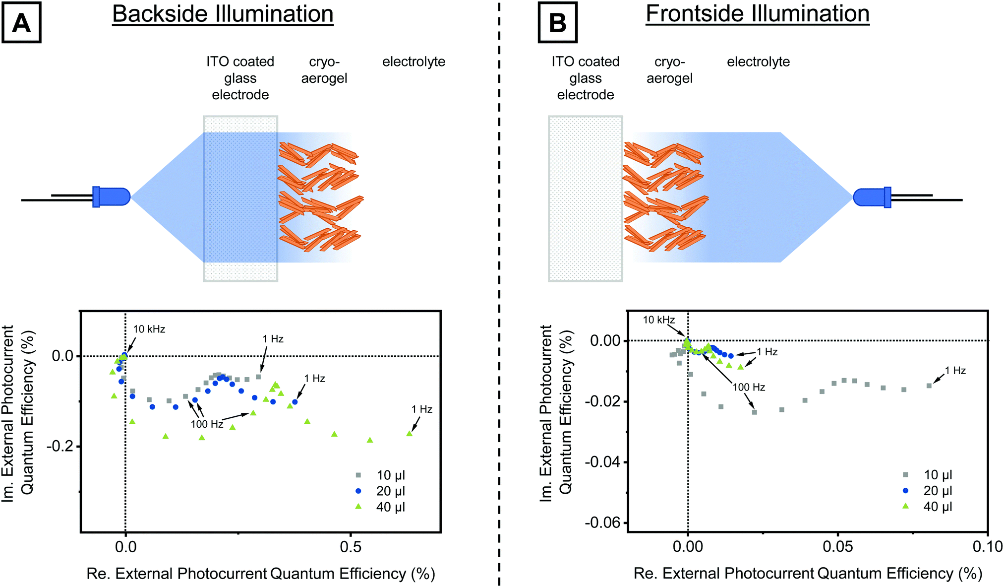 | ||
| Fig. 5 IMPS responses of cryoaerogel coated photoelectrodes with different film thicknesses. For the preparation of all samples, a 28 mM NPL solution dispersed in 1 × 10⁻² M KOH was applied. The samples were irradiated either from the backside (A) or from the frontside (B). The sketches (top) illustrate the differences between both types of irradiation. All IMPS spectra (bottom) were measured at a bias potential of 300 mV. | ||
The radius of the low frequency semicircle shows a strong dependence on the film thickness, too. The radius of this semicircle was observed to be largest for the highest solution amount; and the ratio between the low frequency and the high frequency semicircle also increases with increasing thickness. This implies that the photocurrent contribution of the charge carrier movement, reflected in the low frequency semicircle, increases with increasing film thickness. To further corroborate our interpretation of the low frequency semicircle to be related to the charge carrier movement, we performed similar IMPS experiments with reversed illumination geometry. Due to the frontside illumination, the light intensity gradient is reversed, so that fewer photons reach the particle–electrode interface. Therefore, the ratio of the second (low frequency) and the first (high frequency) semicircle should increase for samples illuminated from the frontside. This indeed was observed for all three film thicknesses as can be seen in Fig. 5B (bottom). From the IMPS plots it can moreover be derived that the highest photocurrent under frontside illumination is generated by the 10 µL sample. The radii of both the higher and the lower frequency semicircles were observed to be much larger than in the case of the thicker cryoaerogel films. The larger high frequency semicircle can be explained by the comparably low optical density of this cryoaerogel film (Fig. S19 and S20, ESI†) and the therefore higher amount of photons passing the outer, less active layers of the cryoaerogel and reaching the particle–substrate interface. The larger low frequency semicircle reveals that not all NPLs of the outer layers contribute equally to the photocurrent. It is more likely that the majority of the charge carriers reaching the electrode surface by diffusion through the NPL network are generated rather close to the electrode surface. The particle–particle contacts in the networks can therefore be considered as diffusion barriers and preferred charge trapping and recombination sites.
Following the afore-mentioned observations and conclusions, an increase of the particle density close to the substrate surface should be beneficial for the photoelectrochemical performance of the cryoaerogel coatings. Cryoaerogels with a higher sheet density could be obtained by increasing the NPL concentration of the applied NPL solution (Fig. 3C). The LSV and the IMPS responses of cryoaerogels fabricated from differently concentrated NPL solutions are shown in Fig. S29 and S30 (ESI†), respectively. The LSVs reveal that the photocurrent of these cryoaerogels is much more closely related to the absolute amount of particles on the electrode than the photocurrent of cryoaerogels with different film thicknesses. In the IMPS responses, an increase of the radius of the high frequency semicircle was observed with increasing NPL concentration. A particularly large difference was registered between the electrodes produced from the 28 mM and 70 mM NPL solutions. We attribute this observation to the morphological differences of both cryoaerogels, especially to the alignment of the sheets in the case of the cryoaerogel fabricated from the 70 mM NPL solution (Fig. 3C). Due to the long-range order of the sheets, channels in the cryoaerogel structure are created, which facilitate the electrolyte diffusion through the cryoaerogel structure. The electrolyte diffusion should further be enhanced by the cracks in the cryoaerogel coating (Fig. S14C, ESI†), which probably result from shrinkage during the drying process.
In conclusion, the highest anodic photocurrents of up to 80 µA cm−2 were observed for the cryoaerogel coated photoelectrodes. This value is comparable to the one reported for a CdSe nanoparticle gel-film26 but significantly larger than all compared values reported for CdSe and CdS nanoparticle mono- and multilayers.5,7,15,33,34,46 The photocurrent direction could be influenced by the solution pH, so that at higher pH also cathodic photocurrents were observed. By means of IMPS it was shown that the majority of the photocurrent is generated directly at the particle–electrode interface by tunnelling processes. However, the IMPS experiments also revealed remarkable photocurrent contributions of charge carrier diffusion processes in the case of the cryoaerogels. These processes are easily distinguishable from the latter ones due to the varying timescales.
Application of NPL cryoaerogel photoelectrodes for photoelectrochemical sensing
In order to prove the applicability of the fabricated cryoaerogel photoelectrodes for photoelectrochemical sensing, we measured the photocurrent response of the electrodes in the presence of differently concentrated ferricyanide solutions. Ferricyanide is a commonly known electron acceptor, which was already applied to demonstrate the electron transfer ability of illuminated semiconductor nanoparticles immobilised on metal photoelectrodes.5 The photocurrent responses of a multilayer and a cryoaerogel photoelectrode to ferricyanide solutions with concentrations between 0 mM (pure phosphate buffer) and 4.3 mM are shown in Fig. 6. It needs to be mentioned that also a (sub-)monolayer coated electrode was exposed to ferricyanide solutions, but only negligible changes in the photocurrent were detected (Fig. S32, ESI†). For the multilayer and the cryoaerogel electrodes, however, increases of the photocurrent of 1.80 µA cm−2 and 6.63 µA cm−2, respectively, were observed in the investigated concentration range. The cryoaerogel photoelectrode showed a remarkably higher sensitivity towards the addition of ferricyanide, so that even concentrations lower than 5 µM could be detected accurately. In contrast, nearly no changes of the photocurrent were measured for the multilayer coated electrode in the low concentration range (Fig. 6B, inset). The multilayer electrodes even showed a slight decrease in the photocurrent at first, which can be explained by a continuous decrease of the blank photocurrent due to particle desorption. The poorer performance of the multilayer photoelectrode is probably related to the fact that the electrolyte as well as the analyte transport to the electrode surface is hampered by the dense nature of the NPL assembly. As revealed by the IMPS measurements, nearly no charge diffusion processes can take place in the multilayer assemblies, so that all photocurrent is generated within a few NPL layers which are within tunnelling distance to the substrate.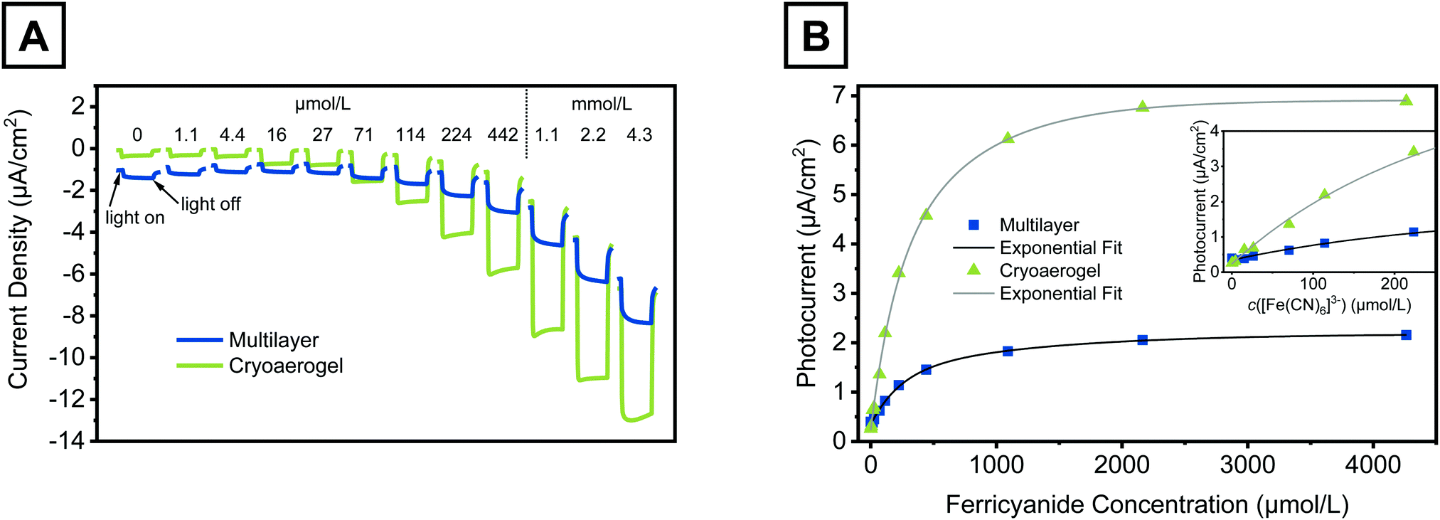 | ||
| Fig. 6 Photocurrent responses of a CdSe NPL multilayer (blue) and a CdSe NPL cryoaerogel coated photoelectrode (green) to ferricyanide solutions with various concentrations. For the preparation of both electrodes, 20 µL of a 28 mM CdSe NPL solution in 1 × 10⁻² M KOH was applied. The experiments were carried out in a 0.1 M HPO42−/H2PO4− buffer (pH 8) at a constant bias potential of −450 mV. (A) Changes in the electrode photocurrent density due to irradiation in the presence of ferricyanide solutions. For each concentration, one representative light pulse with a pulse length of 12.5 s is shown. The total measurement time per concentration was 10 min. Note that the dark current increases with increasing ferricyanide concentration. (B) Dependence of the measured photocurrent on the ferricyanide concentration. Details of the applied fit functions are given in the ESI.† The inset shows the low concentration range up to a ferricyanide concentration of 250 µM. | ||
These conclusions reveal that the application of porous nanoparticle assemblies in photoelectrochemical sensors could lead to significant advances in their performance and their cost-effective production. Further improvements are expected by the application of heterostructured nanoparticles, which are often characterised by more efficient charge carrier separation and longer charge carrier lifetimes.1,47 Assemblies based on heterostructured nanoparticles could also be obtained by cryoaerogelation (Fig. S10, ESI†), as this method is not limited to a specific nanoparticle material or shape.21,38,39
It needs to be mentioned that the developed cryoaerogel photoelectrodes are not selective towards ferricyanide but could in principle detect any reduceable (soluble) analyte with a reduction potential located in the band gap of the CdSe NPLs. A selectivity towards specific analytes could be introduced into this sensing system by functionalisation of the NPLs with biological molecules48–52 or by the addition of shuttle molecules.53,54
Conclusions
In summary, we have shown the preparation of CdSe NPL based cryoaerogel films on photolectrodes and their photoelectrochemical characterisation. By the use of the cryoaerogelation method, CdSe NPL based cryoaerogel films with different thicknesses and morphologies could be obtained. The cryoaerogel films exhibited significantly higher photocurrents than comparable drop-cast films. The IMPS measurements revealed a close relation of the photocurrent enhancement to charge carrier movement, which could solely be proven for the cryoaerogel films. The highest photocurrent efficiencies were observed for the thinnest cryoaerogel films, as well as for cryoaerogel films prepared from highly concentrated NPL solutions. Therefore, IMPS was demonstrated to be a useful photoelectrochemical technique for the characterisation of charge transfer processes in nanoparticle assemblies, which could furthermore facilitate the rational design of these structures.The obtained cryoaerogel photoelectrodes are moreover promising candidates for the fabrication of photoelectrochemical sensors. In a proof-of-priciple experiment, the photoresponse of cryoaerogel photoelectrodes towards ferricyanide was studied. Although both photoelectrodes contained equal amounts of NPLs, cryoaerogel electrodes showed distinctly enhanced sensitivities as well as better photocurrent stabilities compared to drop-cast electrodes. These results suggest that porous NP assemblies such as (cryo)aerogels should be further evaluated as alternatives to particle monolayers and their dense assemblies to enhance the performance of photoelectrochemical sensors in the future.
Conflicts of interest
There are no conflicts of interest to declare.Acknowledgements
The authors would like to acknowledge the German Federal Ministry of Education and Research (BMBF) within the framework of the program NanoMatFutur, support code 03X5525. Furthermore, the project leading to these results has in part received funding from the European Research Council (ERC) under the European Union's Horizon 2020 research and innovation program (grant agreement 714429). In addition, this work was funded by the Deutsche Forschungsgemeinschaft (DFG, German Research Foundation) under Germany's excellence strategy within the cluster of excellence PhoenixD (EXC 2122, project ID 390833453) and the grant BI 1708/4-1. A. S. is thankful for financial support from the Hannover School for Nanotechnology (hsn). The authors moreover thank Rasmus Himstedt for help with TEM analysis, Armin Feldhoff as well as Jürgen Caro for providing the SEM and XRD facilities, and Mandy Jahns and Peter Behrens for krypton physisorption measurements.References
- Z. Yue, F. Lisdat, W. J. Parak, S. G. Hickey, L. Tu, N. Sabir, D. Dorfs and N. C. Bigall, ACS Appl. Mater. Interfaces, 2013, 5, 2800–2814 CrossRef CAS PubMed.
- Y. T. Long, C. Kong, D. W. Li, Y. Li, S. Chowdhury and H. Tian, Small, 2011, 7, 1624–1628 CrossRef CAS PubMed.
- A. Devadoss, P. Sudhagar, C. Terashima, K. Nakata and A. Fujishima, J. Photochem. Photobiol., C, 2015, 24, 43–63 CAS.
- G. L. Wang, P. P. Yu, J. J. Xu and H. Y. Chen, J. Phys. Chem. C, 2009, 113, 11142–11148 CrossRef CAS.
- C. Stoll, S. Kudera, W. J. Parak and F. Lisdat, Small, 2006, 2, 741–743 CrossRef CAS PubMed.
- W. Khalid, M. El Helou, T. Murböck, Z. Yue, J.-M. Montenegro, K. Schubert, G. Göbel, F. Lisdat, G. Witte and W. J. Parak, ACS Nano, 2011, 5, 9870–9876 CrossRef CAS PubMed.
- L. Sheeney-Haj-Ichia, J. Wasserman and I. Willner, Adv. Mater., 2002, 14, 1323–1326 CAS.
- J. Poppe, S. Gabriel, L. Liebscher, S. G. Hickey and A. Eychmüller, J. Mater. Chem. C, 2013, 1, 1515–1524 RSC.
- S. G. Hickey and D. J. Riley, Electrochim. Acta, 2000, 45, 3277–3282 CAS.
- T. Nakanishi, B. Ohtani and K. Uosaki, J. Phys. Chem. B, 1998, 102, 1571–1577 CrossRef CAS.
- X. Yu, Y. Wang, X. Chen, K. Wu, D. Chen, M. Ma, Z. Huang, W. Wu and C. Li, Anal. Chem., 2015, 87, 4237–4244 CrossRef CAS PubMed.
- Z. Yue, W. Khalid, M. Zanella, A. Z. Abbasi, A. Pfreundt, P. Rivera Gil, K. Schubert, F. Lisdat and W. J. Parak, Anal. Bioanal. Chem., 2010, 396, 1095–1103 CAS.
- M. Hojeij, B. Su, S. Tan, G. Mériguet and H. H. Girault, ACS Nano, 2008, 2, 984–992 CrossRef CAS PubMed.
- G. Göbel, K. Schubert, I. W. Schubart, W. Khalid, W. J. Parak and F. Lisdat, Electrochim. Acta, 2011, 56, 6397–6400 CrossRef.
- I. Willner, F. Patolsky and J. Wasserman, Angew. Chem., Int. Ed., 2001, 40, 1861–1864 CrossRef CAS PubMed.
- E. Granot, F. Patolsky and I. Willner, J. Phys. Chem. B, 2004, 108, 5875–5881 CrossRef CAS.
- M. Hojeij, N. Eugster, S. Bin and H. H. Girault, Langmuir, 2006, 22, 10652–10658 CrossRef CAS PubMed.
- J. L. Mohanan, I. U. Arachchige and S. L. Brock, Science, 2005, 307, 397–400 CAS.
- S. Sánchez-Paradinas, D. Dorfs, S. Friebe, A. Freytag, A. Wolf and N. C. Bigall, Adv. Mater., 2015, 27, 6152–6156 CrossRef PubMed.
- S. Naskar, J. F. Miethe, S. Sánchez-Paradinas, N. Schmidt, K. Kanthasamy, P. Behrens, H. Pfnür and N. C. Bigall, Chem. Mater., 2016, 28, 2089–2099 CrossRef CAS.
- A. Freytag, S. Sánchez-Paradinas, S. Naskar, N. Wendt, M. Colombo, G. Pugliese, J. Poppe, C. Demirci, I. Kretschmer, D. W. Bahnemann, P. Behrens and N. C. Bigall, Angew. Chem., Int. Ed., 2016, 55, 1200–1203 CAS.
- I. U. Arachchige and S. L. Brock, J. Am. Chem. Soc., 2007, 129, 1840–1841 CAS.
- V. Lesnyak, S. V. Voitekhovich, P. N. Gaponik, N. Gaponik and A. Eychmüller, ACS Nano, 2010, 4, 4090–4096 CAS.
- V. Sayevich, B. Cai, A. Benad, D. Haubold, L. Sonntag, N. Gaponik, V. Lesnyak and A. Eychmüller, Angew. Chem., Int. Ed., 2016, 55, 6334–6338 CrossRef CAS PubMed.
- N. Gaponik, A. Wolf, R. Marx, V. Lesnyak, K. Schilling and A. Eychmüller, Adv. Mater., 2008, 20, 4257–4262 CAS.
- L. Korala, Z. Wang, Y. Liu, S. Maldonado and S. L. Brock, ACS Nano, 2013, 7, 1215–1223 CrossRef CAS PubMed.
- F. Lübkemann, J. F. Miethe, F. Steinbach, P. Rusch, A. Schlosser, T. Heinemeyer, D. Natke, D. Zok, D. Dorfs and N. C. Bigall, 2019, submitted.
- J. F. Miethe, A. Schlosser, J. G. Eckert, F. Lübkemann and N. C. Bigall, J. Mater. Chem. C, 2018, 6, 10916–10923 RSC.
- J. C. Byers, S. Ballantyne, K. Rodionov, A. Mann and O. A. Semenikhin, ACS Appl. Mater. Interfaces, 2011, 3, 392–401 CAS.
- D. Klotz, D. S. Ellis, H. Dotan and A. Rothschild, Phys. Chem. Chem. Phys., 2016, 18, 23438–23457 RSC.
- L. Dloczik, O. Ileperuma, I. Lauermann, L. M. Peter, E. A. Ponomarev, G. Redmond, N. J. Shaw and I. Uhlendorf, J. Phys. Chem. B, 1997, 101, 10281–10289 CrossRef CAS.
- P. E. de Jongh and D. Vanmaekelbergh, J. Phys. Chem. B, 1997, 101, 2716–2722 CrossRef CAS.
- E. P. A. M. Bakkers, A. L. Roest, A. W. Marsman, L. W. Jenneskens, L. I. de Jong-van Steensel, J. J. Kelly and D. Vanmaekelbergh, J. Phys. Chem. B, 2000, 104, 7266–7272 CrossRef CAS.
- J. F. Miethe, F. Lübkemann, J. Poppe, F. Steinbach, D. Dorfs and N. C. Bigall, ChemElectroChem, 2018, 5, 175–186 CAS.
- M. D. Tessier, P. Spinicelli, D. Dupont, G. Patriarche, S. Ithurria and B. Dubertret, Nano Lett., 2014, 14, 207–213 CrossRef CAS PubMed.
- S. Pedetti, S. Ithurria, H. Heuclin, G. Patriarche and B. Dubertret, J. Am. Chem. Soc., 2014, 136, 16430–16438 CAS.
- T. Kodanek, H. M. Banbela, S. Naskar, P. Adel, N. C. Bigall and D. Dorfs, Nanoscale, 2015, 7, 19300–19309 CAS.
- T. Kodanek, A. Freytag, A. Schlosser, S. Naskar, T. Härtling, D. Dorfs and N. C. Bigall, Z. Phys. Chem., 2018, 232, 1675–1689 CAS.
- A. Freytag, C. Günnemann, S. Naskar, S. Hamid, F. Lübkemann, D. Bahnemann and N. C. Bigall, ACS Appl. Nano Mater., 2018, 1, 6123–6130 CrossRef CAS PubMed.
- K. J. Williams, W. A. Tisdale, K. S. Leschkies, G. Haugstad, D. J. Norris, E. S. Aydil and X. Y. Zhu, ACS Nano, 2009, 3, 1532–1538 CrossRef CAS PubMed.
- M. J. Berr, P. Wagner, S. Fischbach, A. Vaneski, J. Schneider, A. S. Susha, A. L. Rogach, F. Jäckel and J. Feldmann, Appl. Phys. Lett., 2012, 100, 223903 Search PubMed.
- M. J. Berr, A. Vaneski, C. Mauser, S. Fischbach, A. S. Susha, A. L. Rogach, F. Jäckel and J. Feldmann, Small, 2012, 8, 291–297 CrossRef CAS PubMed.
- D. Spittel, J. Poppe, C. Meerbach, C. Ziegler, S. G. Hickey and A. Eychmüller, ACS Nano, 2017, 11, 12174–12184 CrossRef CAS PubMed.
- A. Antanovich, A. Prudnikau, A. Matsukovich, A. Achtstein and M. Artemyev, J. Phys. Chem. C, 2016, 120, 5764–5775 CrossRef CAS.
- L. M. Peter, J. Li, R. Peat, H. J. Lewerenz and J. Stumper, Electrochim. Acta, 1990, 35, 1657–1664 CAS.
- N. A. Kotov, I. Dekany and J. H. Fendler, J. Phys. Chem., 1995, 99, 13065–13069 CAS.
- F. Rajadell, J. I. Climente and J. Planelles, Phys. Rev. B, 2017, 96, 035307 CrossRef.
- V. Pardo-Yissar, E. Katz, J. Wasserman and I. Willner, J. Am. Chem. Soc., 2003, 125, 622–623 CAS.
- W. W. Zhao, P. P. Yu, J. J. Xu and H. Y. Chen, Electrochem. Commun., 2011, 13, 495–497 CrossRef CAS.
- X. Zhang, S. Li, X. Jin and S. Zhang, Chem. Commun., 2011, 47, 4929–4931 RSC.
- G. L. Wang, J. J. Xu, H. Y. Chen and S. Z. Fu, Biosens. Bioelectron., 2009, 25, 791–796 CAS.
- G. L. Wang, P. P. Yu, J. J. Xu and H. Y. Chen, J. Phys. Chem. C, 2009, 113, 11142–11148 CrossRef CAS.
- C. Stoll, C. Gehring, K. Schubert, M. Zanella, W. J. Parak and F. Lisdat, Biosens. Bioelectron., 2008, 24, 260–265 CrossRef CAS PubMed.
- E. Katz, M. Zayats, I. Willner and F. Lisdat, Chem. Commun., 2006, 1395–1397 RSC.
Footnote |
| † Electronic supplementary information (ESI) available. See DOI: 10.1039/c9cp00281b |
| This journal is © the Owner Societies 2019 |