
Functionalized MXenes as ideal electrodes for Janus MoSSe
Yuanyuan
Wang
,
Wei
Wei
 *,
Baibiao
Huang
and
Ying
Dai
*
*,
Baibiao
Huang
and
Ying
Dai
*
School of Physics, State Key Laboratory of Crystal Materials, Shandong University, Jinan 250100, China. E-mail: weiw@sdu.edu.cn; daiy60@sdu.edu.cn
First published on 21st November 2018
Abstract
On the basis of first-principles calculations, we examined the possibility of functionalized transition metal carbides and nitrides (f-MXenes) as ideal electrode materials for two-dimensional (2D) Janus MoSSe through interfacial electronic properties and Schottky barriers within MoSSe/f-MXene van der Waals (vdW) heterostructures. We found that the interactions between MoSSe and f-MXenes are weak, and thus the intrinsic electronic features of MoSSe could be reserved. Based on band structure calculations, the minus n-type (vanishing) Schottky barrier heights could be assigned to MoSSe/Ti2C(OH)2 and MoSSe/Mo2C(OH)2, and the p-type Schottky barrier height assigned to Sc2NO2 turns out to be negligible. When taking the charge redistribution at the interfaces into account, our band structure results are consistent with the modified Schottky–Mott equation. Our work provides a reference for selecting ideal electrode materials and channel materials for electronic applications.
1. Introduction
Semiconductor devices based on two-dimensional (2D) materials have drawn increasing attention due to their fascinating properties. Atom-thick 2D semiconductors with dangling-bond-free surfaces are considered to be one of the most promising candidates as channel materials for future ultra-small scale electronics.1 However, in 2D semiconductor/metal heterostructures, the Fermi level pinning is strong, which means that the Fermi level varies slightly when using different gate voltages to regulate it, resulting in a gate-voltage untunable Schottky barrier height (SBH).2–4 The strong Fermi level pinning hinders the formation of low-resistance contacts, discourages the gate electrostatic control and masks the intrinsic exceptional electronic properties of the 2D semiconductors.2,5 As a consequence, high resistance exists within the device due to the generated Schottky barriers at the interface between the electrode and channel regions, thus the Schottky barriers will impede the carriers’ transport and degrade the device performance.It has been widely recognized that combining different 2D materials to construct van der Waals (vdW) heterostructures with designed electronic properties will bring new and exciting physical phenomena, which is now a central concept for nanoscale electronic and photovoltaic devices. It has also been demonstrated that Fermi level pinning can be weakened by using 2D metals to form vdW heterostructures with 2D channel materials, giving rise to a tunable Schottky barrier height.6,7 However, stable and reliable doping strategies to reduce the contact resistance between 2D semiconductor and 2D metal contacts are currently lacking,8 and exploration of suitable 2D metals and contact configurations with excellent potential to form low-resistance contacts is still highly expected. Therefore, it is quite challenging to select an appropriate 2D metallic material as the contact electrode to construct heterostructures with 2D channel materials, where an ideal case is that the Schottky barrier disappears.
2D Janus materials with different atoms on two faces have received rapidly increasing attention. The mirror asymmetry of Janus structures introduces the out-of-plane polarized electric field and will further enhance the out-of-piezoelectric coefficients due to the large change in polarization under in-plane strain. For example, group-III monochalcogenides were predicted as promising candidates for piezoelectronics.9 In addition, graphene-based materials modified by different functional groups have been regarded as ideal materials for field-effect transistors and Li–S batteries.10 The Janus structure of transition metal dichalcogenides (TMDs), namely MoSSe, was successfully synthesized recently.11,12 Different from 2D TMDs with mirror symmetry (e.g., MoS2 and MoSe2), Janus MoSSe shows an intrinsic out-of-plane electric field due to the mirror asymmetry, which leads to new properties that MoS2 and MoSe2 may not hold and has generated a surge of interest. The structural stability, electronic properties, valley polarization, Rashba effect and optical properties of MoSSe have been widely studied.12–16 In addition, previous works indicated that MoSSe has great potential in applications such as catalysis, optoelectronics, spintronics, valleytronics and piezoelectronics.16–21 A sizable direct band gap within the visible frequency is assigned to MoSSe, and the carrier mobility is predicted to be higher than that of MoS2 in previous calculations.14 However, there is conflict about the carrier mobility. For example, some works indicate that the carrier mobility of MoSSe is lower than that of MoS2.19,22 It is of interest that the dangling-bond-free surface and atomic thickness can provide gate electrostatic controllability to suppress the short channel effects, and therefore MoSSe could be a suitable channel material for electronic applications.23,24
In the light of metallic characters and high conductivity, the newly discovered 2D transition metal carbides and nitrides (known as MXenes, such as Ti2C, Mo2C and Sc2N) show promise as contact electrodes.25–27 It has been identified that 2D semiconductors interact strongly with bare MXenes, and the bands of the semiconductors are significantly perturbed with respect to the band edges of the original gap region.28,29 In this case, 2D semiconductors turn out to be metallic. But, strong interactions and the electronic state hybridization of the contacting components could strongly destroy the band dispersion of the 2D semiconductors, indicating that bare MXenes are not ideal electrode materials for common 2D semiconductors. However, functionalized MXenes (f-MXenes) can predominantly preserve the band characteristics of the 2D semiconductors.28,29 As electrode materials, f-MXenes exhibit many advantages superior to conventional metals so that they offer numerous opportunities as electrode candidates for 2D channel materials such as MoSSe. Thus, it is highly desirable to have a comprehensive understanding of the electronic properties and interface characteristics of MoSSe/f-MXene heterostructures and find appropriate systems to achieve the low-resistance.
In this work, from the device point of view, we calculated two primary parameters determining the carrier injection efficiency for MoSSe/f-MXene heterostructures, SBH and tunneling barriers.8,29,30 Our results indicate that f-MXenes are promising candidate electrodes for MoSSe due to the absence of Schottky barrier and a tolerable tunneling barrier. The band calculations are consistent with the results of the modified Schottky–Mott model theory, and the position of the Fermi level with respect to the band edge is adjustable in MoSSe/f-MXene heterostructures, so that the nature of the Schottky barrier is controllable. Our study could shed some light on MoSSe/f-MXene vdW heterostructures in device applications.
2. Computational method
The density functional theory (DFT) calculations were performed using the Vienna ab initio Simulation Package (VASP).31 All the calculations were carried out using the Perdew–Burke–Ernzerhof (PBE) exchange–correlation functional in the framework of the generalized gradient approximation (GGA),32 and the projector augmented wave (PAW)33 was adopted for the electron–ion interactions. Considering that the PBE functional always underestimates the band gap, we also calculated the electronic band structures using the Heyd–Scuseria–Ernzerhof (HSE06)34 hybrid functional to verify the reliability of our conclusions, since the HSE06 functional has been proven to provide more accurate band gaps and band edge positions.35 The cut-off kinetic energy for plane waves was set to 450 eV. The structures were fully relaxed until the force on each atom was less than 0.01 eV Å−1 and the convergence tolerance for energy was 10−5 eV. A Monkhorst–Pack k-point mesh of 13 × 13 × 1 was used to sample the Brillouin zone for geometry optimization and static electronic structure calculations.36 In order to take the vdW interactions into account for the heterostructures, DFT-D2 corrections within the PBE functional were performed to give more accurate results.37–39 The dipole corrections perpendicular to the interfaces of heterostructures were considered.15,39 A vacuum space of 18 Å was added in the direction normal to the interfaces of MoSSe/f-MXenes.3. Results and discussion
It is known that f-MXenes mainly exhibit four possible models, proposed by Khazaei et al.40 In the present work, only the most stable phase that was confirmed in previous works is taken into account.41,42 In Fig. 1a, atomic coordinates of MoSSe and f-MXenes are shown. The optimized lattice parameters for MoSSe, Ti2C(OH)2, Mo2C(OH)2 and Sc2NO2 are 3.25, 3.07, 3.28 and 3.25 Å, respectively, which are in good agreement with previous studies.14,41,42 It can be observed that there is a smaller lattice mismatch between MoSSe and f-MXenes, with a relatively large one for MoSSe/Ti2C(OH)2 of 5.86%. In order to compensate the effects induced by the lattice mismatch, the lattice parameter of MoSSe is kept fixed (3.25 Å) since the electronic properties of MoSSe are very sensitive to strain.19 In this case, Ti2C(OH)2 will experience tensile strain (5.86%), while strains applied to Mo2C(OH)2 and Sc2NO2 are negligible with MoSSe being strain-free. The introduced strain can largely influence the electronic properties of the materials and play an important role in determining the contact features. Related theoretical research shows that f-MXenes can maintain mechanical flexibility under large strain, which is another reason for applying strain on f-MXenes in this work.27 This strategy was also adopted in the previous study on the TiS3/graphene heterostructure,8 where the lattice parameter of TiS3 was kept fixed as its free-standing case. It should be pointed out that the lattice parameters of a heterostructure are related to its mechanical strength and should be determined by how the heterostructure is grown or fabricated. Fig. 1b shows the band structure of free-standing MoSSe, and the band gap at the PBE level of theory is 1.56 eV. Our results also indicate that when applying a strain of 5.86%, the isolated Ti2C(OH)2 monolayer retains metallic characteristics, as shown in Fig. 1c and d. In addition, isolated Mo2C(OH)2 and Sc2NO2 monolayers have also been confirmed to be metallic, which is in agreement with previous results.41 | ||
| Fig. 1 (a) Models of 2D Janus MoSSe and f-MXenes, OH* is replaced by O* in Sc2NO2. Band structures of (b) MoSSe, (c) strain-free Ti2C(OH)2 and (d) Ti2C(OH)2 with a tensile strain of 5.86%; the Fermi level is set to zero. | ||
Considering that the position of f-MXenes with respect to MoSSe finds several choices, we therefore take six high symmetry stacking types into account to get the most stable configurations. Fig. 2 shows the representative MoSSe/Mo2C(OH)2 vdW heterostructures, which are referred to as hcp-I (II), top-I (II) and fcc-I (II). It can be found that hcp-I (II) has all C atoms directly above S atoms, top-I (II) has all C atoms on top of Mo atoms, and fcc-I (II) shows that OH is located on top of S (Mo). In consideration of the fact that the mirror asymmetry of MoSSe with either S or Se could be the interface atoms, there are indeed 12 configurations for each of the MoSSe/f-MXene vdW heterostructures.
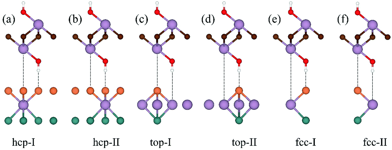 | ||
| Fig. 2 Staking orders of MoSSe/f-MXenes. | ||
To further determine the stability of the vdW heterostructures, the interface formation energies are calculated as
| Eb = E(vdWH) − E(MoSSe) − E(f-MXenes) |
| hcp-I | hcp-II | top-I | top-II | fcc-I | fcc-II | ||
|---|---|---|---|---|---|---|---|
| MoSSe/Ti2C(OH)2 | S | −2.010 | −2.020 | −2.024 | −2.003 | −1.999 | −2.024 |
| Se | −1.984 | −1.976 | −1.988 | −1.946 | −1.936 | −1.986 | |
| MoSSe/Mo2C(OH)2 | S | −2.455 | −2.462 | −2.459 | −2.460 | −2.462 | −2.465 |
| Se | −2.413 | −2.407 | −2.414 | −2.380 | −2.381 | −2.409 | |
| MoSSe/Sc2NO2 | S | −1.739 | −1.714 | −1.740 | −1.656 | −1.660 | −1.727 |
| Se | −1.803 | −1.786 | −1.789 | −1.699 | −1.701 | −1.785 | |
Fig. 3a–c present the projected band structures of the MoSSe/f-MXene vdW heterostructures (at the PBE level of theory). It is visualized that after contacting with Ti2C(OH)2 and Mo2C(OH)2, the band structure of MoSSe is basically unperturbed with a gap of 1.56 eV. Yet the band gap of MoSSe slightly changes to 1.49 eV in the case of MoSSe/Sc2NO2. It can be found that the individual bands for isolated MoSSe and f-MXenes are distinguishable from the band structures of the heterostructures, and the electronic structures of both MoSSe and MXenes are well preserved (see Fig. 3d–f). The results reveal the weak interactions between MoSSe and f-MXenes, which can also be visualized through the electron localization functions (ELFs). As shown in Fig. 4 of the ELFs of these heterostructures, no covalent bonds form between MoSSe and f-MXenes, verifying the weak interactions. On the basis of the HSE06 functional, the band structures of MoSSe/Ti2C(OH)2, MoSSe/Mo2C(OH)2 and MoSSe/Sc2NO2 indicate that the band gap of MoSSe increases to 1.91, 1.89 and 1.89 eV, respectively. However, the band dispersions remain virtually unchanged.
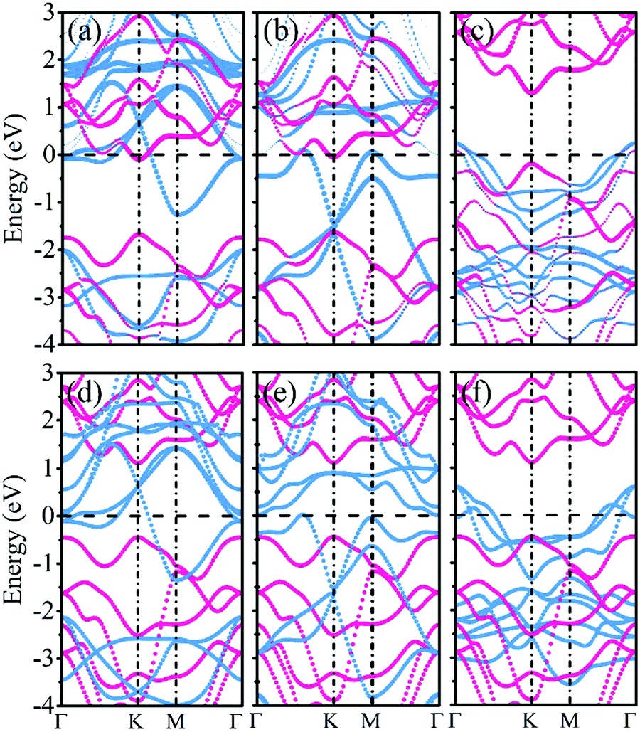 | ||
| Fig. 3 Projected band structures (top) and superposed band structures (bottom) of (a), (d) MoSSe/Ti2C(OH)2, (b), (e) MoSSe/Mo2C(OH)2 and (c), (f) MoSSe/Sc2NO2; red and blue denote the bands of MoSSe and f-MXenes, respectively, and the Fermi level is set to zero. | ||
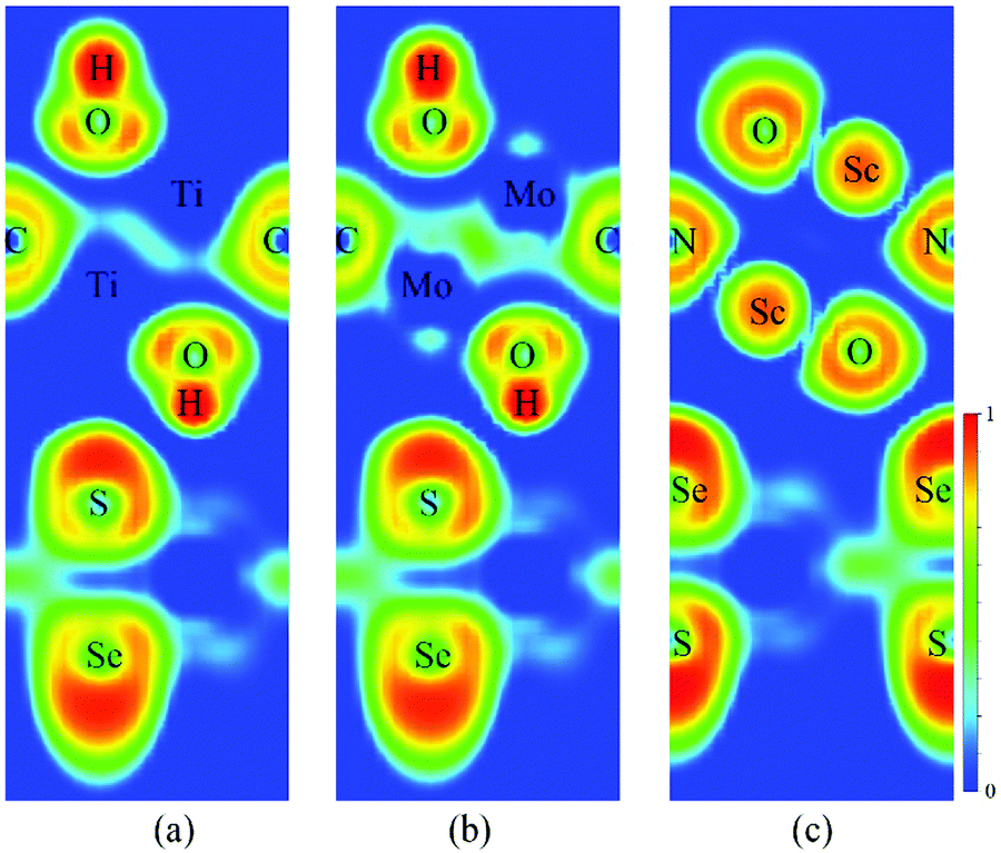 | ||
| Fig. 4 Electron localization functions (ELFs) of (a) MoSSe/Ti2C(OH)2, (b) MoSSe/Mo2C(OH)2 and (c) MoSSe/Sc2NO2. | ||
From the point of view of devices, one of the most crucial characteristics of semiconductor–metal contacts is the SBH when using metallic f-MXenes as electrodes and semiconducting MoSSe as channels. The Schottky barrier is generally determined by the energy difference between the Fermi level and the semiconductor band edges at the metal/semiconductor interfaces. Therefore, a p-type Schottky barrier (ΦBp) is defined by the energy difference between the Fermi level and the valence band maximum (VBM) of the semiconductor, and an n-type Schottky barrier (ΦBn) is measured by the energy difference between the conduction band minimum (CBM) of the semiconductor and the Fermi level. When ΦBp or ΦBn is negative with a vanishing SBH, it will be an Ohmic contact. In other words, when the CBM or VBM contacts the Fermi level, an Ohmic contact will be generated at the interfaces of the heterostructures. A vanishing ΦBn (ΦBp) implies the spontaneous injection of electrons (holes) from f-MXenes to MoSSe. In Fig. 3a and b, it can be observed that the CBM of MoSSe is located just below the Fermi level, showing a Schottky-barrier-free contact and spontaneous electron transfer from Ti2C(OH)2 (ΦBn = −0.105 eV) and Mo2C(OH)2 (ΦBn = −0.048 eV) to MoSSe. Yet, it can be seen that the VBM of MoSSe is very close to the Fermi level in the case of MoSSe/Sc2NO2, forming a p-type Schottky contact with a small barrier (ΦBp = 0.189 eV), as illustrated in Fig. 3c.
For bulk metal/semiconductor contacts, it is difficult to regulate the vanishing Schottky barriers in most cases as a result of the strong bonding, which leads to Fermi level pinning at the interfaces. This problem is usually treated by inserting an insulating monolayer into the interface to weaken the strong interactions and reduce the interface states.43 However, such an approach involves great complexity in experiments. By comparison, the functionalized groups are more easily intercalated into the MoSSe/MXene interfaces because the synthesis of MXenes is a self-assembly process where chemical groups can spontaneously cover the surfaces. This suggests the experimental feasibility for the synthesis of MoSSe/f-MXene vdW heterostructures with vanishing Schottky barriers.
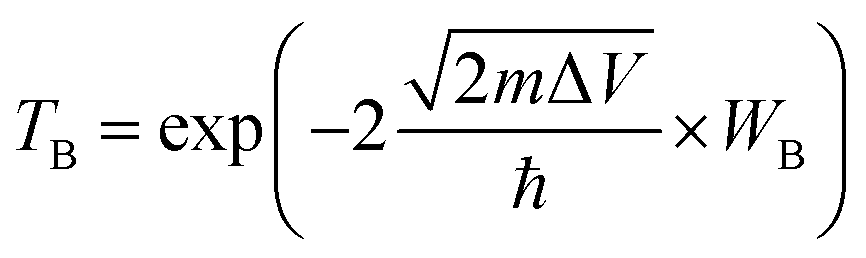
Tunneling barrier is another important index to measure the performance of devices and is usually characterized by two important parameters: barrier width (WB) and barrier height (ΔV).8,44 As shown in Fig. 5a–c of the potential profiles, in which the average electrostatic potential of the whole system is set as the reference (zero level) for the Fermi level and the subsequent work function, electron affinity and ionization potential. As a relative quantity, it can also be used as the reference to calculate the height/width of the tunneling barrier. As a result, the barrier height (ΔV) can be defined as the electrostatic potential at the interface region with the zero level as the reference. In this regard, barrier height (ΔV) and barrier width (WB) form as electrons cross the vdW gap at the interface, which can be measured by the electrostatic potential. There is an obvious tunneling barrier at the interfaces with barrier heights of 2.3, 2.7 and 2.5 eV for MoSSe/Ti2C(OH)2, MoSSe/Mo2C(OH)2 and MoSSe/Sc2NO2, respectively. Here, we calculated the possibility of tunneling (TB) by replacing the irregular real barriers with square barriers according to8,44,45
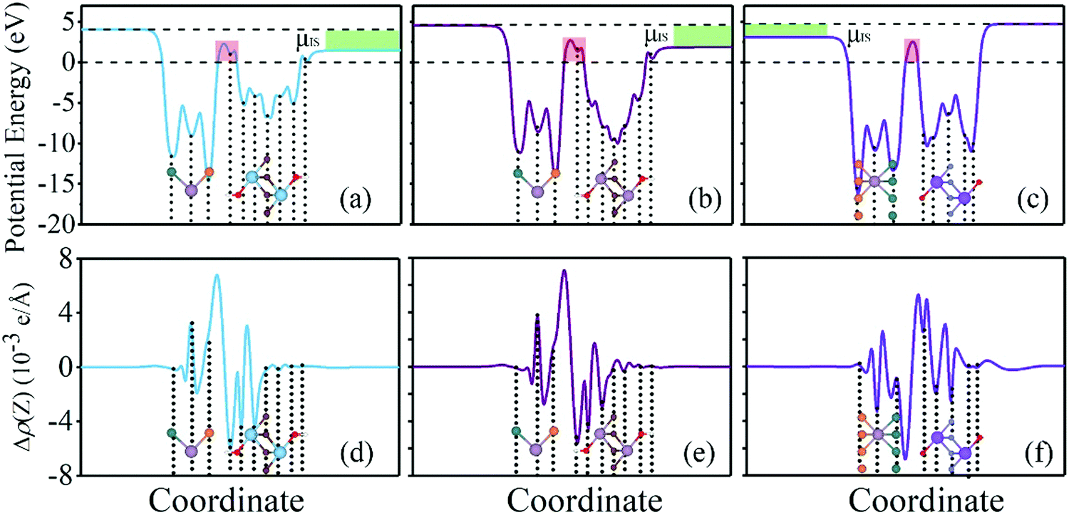 | ||
| Fig. 5 Potential profiles of (a) MoSSe/Ti2C(OH)2, (b) MoSSe/Mo2C(OH)2 and (c) MoSSe/Sc2N(O)2; red rectangular boxes indicate the tunneling barrier. Charge density difference between MoSSe and (d) Ti2C(OH)2, (e) Mo2C(OH)2 and (f) Sc2NO2. | ||
| ΔV (eV) | W B (Å) | T B (%) | |
|---|---|---|---|
| MoSSe/Ti2C(OH)2 | 2.3 | 1.74 | 6.72 |
| MoSSe/Mo2C(OH)2 | 2.7 | 1.82 | 4.69 |
| MoSSe/Sc2N(O)2 | 2.5 | 1.33 | 11.65 |
The Schottky barriers can be intuitively obtained by the difference between the band edges of the heterostructures and the Fermi level. In addition, the Schottky–Mott equation is an alternative to calculate the Schottky barriers involving the work function of f-MXenes. After calculating the Schottky barriers of the heterostructures based on the band structures, the underlying mechanism determining the Schottky barrier at the interfaces of MoSSe/f-MXenes will be demonstrated. The planar-average electrostatic potential of MoSSe is shown in Fig. 6a; a discontinuity of 0.75 eV between two vacuum levels (S and Se sides) can be acquired; in fact it is also the work function difference between the S and Se layers. Fig. 6b shows the work functions of isolated f-MXenes and their relative positions with respect to the band edges of MoSSe, also taking the work function discontinuity in MoSSe into account. In Fig. 6b, the difference between the vacuum level and green lines represents the work function of isolated f-MXenes, while the difference between the vacuum level and the Fermi level can be considered as the work function of isolated MoSSe. The relative positions of the band edges can be determined from the band structures. As shown in Fig. 6b, the work functions of f-MXenes are higher/lower than those of MoSSe, thus the anti-blocking layers formed for majority carriers and electrons/holes will transmit to the opposite layers without barriers. It is observed that Ti2C(OH)2 and Mo2C(OH)2 have relatively low work functions, with the Fermi levels located above the CBM of MoSSe, while Sc2NO2 with a relatively high work function has the Fermi level below the VBM of MoSSe. The Schottky–Mott rule is indicative of the relationship between the work functions of the electrode materials and Schottky barriers, it can be written as46
| ΦBn = WM − Eea, ΦBP = Eip − WM |
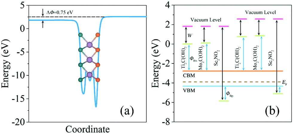 | ||
| Fig. 6 (a) Planar-average electrostatic potential of MoSSe. (b) Energy alignment for isolated f-MXenes and MoSSe. The work function and the Schottky barrier are denoted, with both Se (left part) and S (right part) surfaces being considered. | ||
The electronegativity difference between the interface atoms leads to interface charge rearrangement. In addition, tunneling effects also play a role in affecting the interface charge rearrangement. Accordingly, the interface dipole and charge rearrangement at the interface of MoSSe/f-MXene vdW heterostructures are examined. The charge redistribution at the interface is determined based on the following equation:
| Δρ = ρ(vdWH) − ρ(MoSSe) − ρ(f-MXenes) |
| ΦBn = WM − Eea + μIS, ΦBP = Eip − WM − μIS |
Our results indicate that when considering the vacuum level for the Se side, the SBH values are −0.18, 0.21 and 0.12 eV for Ti2C(OH)2, Mo2C(OH)2 and MoSSe/Sc2NO2, respectively, which are consistent with the band structure results. It thus suggests that the interface dipole moment because of the charge rearrangement will largely influence the SBH. The small deviation may result from the weak interlayer hybridizations.47 Recently, theoretical studies demonstrated the strong interactions between bare MXenes and the channel materials (e.g., ReS2, GaSe and MoS2), leading to the Fermi level pinning effect.29,48,49 Unlike bare MXenes, combining f-MXenes and channel materials can form vdW heterostructures, which effectively avoids the Fermi level pinning effect. Comparing with other channel materials, MoSSe shows potential to adjust the type of majority carriers due to the ideal n-type and negligible p-type SBH.
4. Conclusions
In conclusion, MoSSe/Ti2C(OH)2, MoSSe/Mo2C(OH)2 and MoSSe/Sc2NO2 vdW heterostructures with well-preserved band dispersions exhibit negligible or even minus Schottky barriers. Our results indicate that the vdW heterostructures show the possibility of tunneling, so that they can be used as potential electrical contact materials. However, band calculations deviate from the Schottky–Mott rule due to the interface dipole in the heterostructures related to the charge redistribution at the interface. Our results suggest that the band structure results are consistent with the modified Schottky–Mott equation.Conflicts of interest
There are no conflicts to declare.Acknowledgements
This work is supported by the National Natural Science Foundation of China (No. 51872170, 11374190 and 21333006), the Taishan Scholar Program of Shandong Province, and the Young Scholars Program of Shandong University (YSPSDU).Notes and references
- F. Schwierz, J. Pezoldt and R. Granzner, Nanoscale, 2015, 7, 8261–8283 RSC.
- J. Su, L. Feng, W. Zeng and Z. Liu, Nanoscale, 2017, 9, 7429–7441 RSC.
- X. Zhang, Y. Pan, M. Ye, R. Quhe, Y. Wang, Y. Guo, H. Zhang, Y. Dan, Z. Song, J. Li, J. Yang, W. Guo and J. Lu, Nano Res., 2017, 11, 707–721 CrossRef.
- J. Z. Li, X. T. Sun, C. Y. Xu, X. Y. Zhang, Y. Y. Pan, M. Ye, Z. G. Song, R. G. Quhe, Y. Y. Wang, H. Zhang, Y. Guo, J. B. Yang, F. Pan and J. Lu, Nano Res., 2018, 11, 1834–1849 CrossRef CAS.
- R. Quhe, Y. Wang, M. Ye, Q. Zhang, J. Yang, P. Lu, M. Lei and J. Lu, Nanoscale, 2017, 9, 14047–14057 RSC.
- Y. Liu, P. Stradins and S. H. Wei, Sci. Adv., 2016, 2, e1600069 CrossRef.
- J. E. Padilha, A. Fazzio and A. J. da Silva, Phys. Rev. Lett., 2015, 114, 066803 CrossRef CAS PubMed.
- J. Liu, Y. Guo, F. Q. Wang and Q. Wang, Nanoscale, 2018, 10, 807–815 RSC.
- Y. Guo, S. Zhou, Y. Bai and J. Zhao, Appl. Phys. Lett., 2017, 110, 163102 CrossRef.
- S.-W. Ng, N. Noor and Z. Zheng, NPG Asia Mater., 2018, 10, 217–237 CrossRef CAS.
- Y. Lu, H. Zhu, J. Xiao, C. P. Chuu, Y. Han, M. H. Chiu, C. C. Cheng, C. W. Yang, K. H. Wei, Y. Yang, Y. Wang, D. Sokaras, D. Nordlund, P. Yang, D. A. Muller, M. Y. Chou, X. Zhang and L. J. Li, Nat. Nanotechnol., 2017, 12, 744 CrossRef.
- J. Zhang, S. Jia, I. Kholmanov, L. Dong, D. Er, W. Chen, H. Guo, Z. Jin, V. B. Shenoy, L. Shi and J. Lou, ACS Nano, 2017, 11, 8192–8198 CrossRef CAS PubMed.
- Y. C. Cheng, Z. Y. Zhu, M. Tahir and U. Schwingenschlögl, EPL, 2013, 102, 57001 CrossRef.
- J. Wang, H. Shu, T. Zhao, P. Liang, N. Wang, D. Cao and X. Chen, Phys. Chem. Chem. Phys., 2018, 20, 18571–18578 RSC.
- F. Li, W. Wei, P. Zhao, B. Huang and Y. Dai, J. Phys. Chem. Lett., 2017, 8, 5959–5965 CrossRef CAS PubMed.
- R. Peng, Y. Ma, S. Zhang, B. Huang and Y. Dai, J. Phys. Chem. Lett., 2018, 9, 3612–3617 CrossRef CAS.
- D. Er, H. Ye, N. C. Frey, H. Kumar, J. Lou and V. B. Shenoy, Nano Lett., 2018, 18, 3943–3949 CrossRef CAS.
- Y. J. Ji, M. Y. Yang, H. P. Lin, T. J. Hou, L. Wang, Y. Y. Li and S. T. Lee, J. Phys. Chem. C, 2018, 122, 3123–3129 CrossRef CAS.
- X. Ma, X. Wu, H. Wang and Y. Wang, J. Mater. Chem. A, 2018, 6, 2295–2301 RSC.
- Y. Liang, J. Li, H. Jin, B. Huang and Y. Dai, J. Phys. Chem. Lett., 2018, 9, 2797–2802 CrossRef CAS.
- L. Dong, J. Lou and V. B. Shenoy, ACS Nano, 2017, 11, 8242–8248 CrossRef CAS.
- Y. Cai, G. Zhang and Y. W. Zhang, J. Am. Chem. Soc., 2014, 136, 6269–6275 CrossRef CAS PubMed.
- B. Radisavljevic, A. Radenovic, J. Brivio, V. Giacometti and A. Kis, Nat. Nanotechnol., 2011, 6, 147 CrossRef CAS.
- M. Chhowalla, D. Jena and H. Zhang, Nat. Rev. Mater., 2016, 1, 11 Search PubMed.
- J. Halim, S. Kota, M. R. Lukatskaya, M. Naguib, M. Q. Zhao, E. J. Moon, J. Pitock, J. Nanda, S. J. May, Y. Gogotsi and M. W. Barsoum, Adv. Funct. Mater., 2016, 26, 3118–3127 CrossRef CAS.
- M. Khazaei, M. Arai, T. Sasaki, M. Estili and Y. Sakka, Phys. Chem. Chem. Phys., 2014, 16, 7841–7849 RSC.
- M. Khazaei, A. Ranjbar, M. Arai, T. Sasaki and S. Yunoki, J. Mater. Chem. C, 2017, 5, 2488–2503 RSC.
- H. Wang, C. Si, J. Zhou and Z. Sun, J. Phys. Chem. C, 2017, 121, 25164–25171 CrossRef CAS.
- P. Zhao, H. Jin, X. Lv, B. Huang, Y. Ma and Y. Dai, Phys. Chem. Chem. Phys., 2018, 20, 16551–16557 RSC.
- X. Lv, W. Wei, P. Zhao, J. Li, B. Huang and Y. Dai, Phys. Chem. Chem. Phys., 2018, 20, 1897–1903 RSC.
- G. Kresse and J. Furthmüller, Phys. Rev. B: Condens. Matter Mater. Phys., 1996, 54, 11169 CrossRef CAS.
- J. P. Perdew, K. Burke and M. Ernzerhof, Phys. Rev. Lett., 1996, 77, 3865 CrossRef CAS.
- G. Kresse, Phys. Rev. B: Condens. Matter Mater. Phys., 1999, 59, 1758 CrossRef CAS.
- J. Heyd, G. E. Scuseria and M. Ernzerhof, J. Chem. Phys., 2003, 118, 8207 CrossRef CAS.
- X. H. Zha, Q. Huang, J. He, H. He, J. Zhai, J. S. Francisco and S. Du, Sci. Rep., 2016, 6, 27971 CrossRef.
- H. J. Monkhorst and J. D. Pack, Phys. Rev. B: Condens. Matter Mater. Phys., 1976, 13, 5188 CrossRef.
- L.-Y. Gan, Q. Zhang, Y. Cheng and U. Schwingenschlögl, Phys. Rev. B: Condens. Matter Mater. Phys., 2013, 87, 245307 CrossRef.
- G. Graziano, J. Klimes, F. Fernandez-Alonso and A. Michaelides, J. Phys.: Condens. Matter, 2012, 24, 424216 CrossRef.
- G. Makov and M. C. Payne, Phys. Rev. B: Condens. Matter Mater. Phys., 1995, 51, 4014 CrossRef CAS.
- M. Khazaei, M. Arai, T. Sasaki, C.-Y. Chung, N. S. Venkataramanan, M. Estili, Y. Sakka and Y. Kawazoe, Adv. Funct. Mater., 2013, 23, 2185 CrossRef CAS.
- H. A. Tahini, X. Tan and S. C. Smith, Nanoscale, 2017, 9, 7016–7020 RSC.
- U. Yorulmaz, A. Ozden, N. K. Perkgoz, F. Ay and C. Sevik, Nanotechnology, 2016, 27, 335702 CrossRef PubMed.
- J. Su, L. P. Feng, X. Zheng, C. Hu, H. Lu and Z. Liu, ACS Appl. Mater. Interfaces, 2017, 9, 40940 CrossRef CAS PubMed.
- Y. Pan, Y. Wang, M. Ye, R. Quhe, H. Zhong, Z. Song, X. Peng, D. Yu, J. Yang, J. Shi and J. Lu, Chem. Mater., 2016, 28, 2100–2109 CrossRef CAS.
- X. Ji, J. Zhang, Y. Wang, H. Qian and Z. Yu, Phys. Chem. Chem. Phys., 2013, 15, 17883–17886 RSC.
- Y. Liu, H. Xiao and W. A. Goddard, J. Am. Chem. Soc., 2016, 138, 15853–15856 CrossRef CAS.
- R. T. Tung, Phys. Rev. B: Condens. Matter Mater. Phys., 2001, 64, 205310 CrossRef.
- N. Gao, S. Zhou, N. Liu, Y. Bai and J. Zhao, J. Mater. Chem. C, 2018, 6, 6764–6770 RSC.
- N. Liu, S. Zhou, N. Gao and J. Zhao, Phys. Chem. Chem. Phys., 2018, 20, 21732–21738 RSC.
| This journal is © the Owner Societies 2019 |