
 Open Access Article
 This Open Access Article is licensed under a Creative Commons Attribution-Non Commercial 3.0 Unported Licence
Anisotropic mosaicity and lattice-plane twisting of an m-plane GaN homoepitaxial layer
Jaemyung
Kim
abc,
Okkyun
Seo
abc,
Atsushi
Tanaka
d,
Jun
Chen
a,
Kenji
Watanabe
 a,
Yoshio
Katsuya
b,
Toshihide
Nabatame
a,
Yoshihiro
Irokawa
a,
Yasuo
Koide
a and
Osami
Sakata
*abc
a,
Yoshio
Katsuya
b,
Toshihide
Nabatame
a,
Yoshihiro
Irokawa
a,
Yasuo
Koide
a and
Osami
Sakata
*abc
aCenter for GaN Characterization, Research Network and Facility Services Division (RNFS), National Institute for Materials Science (NIMS), Tsukuba, Ibaraki, 305-0047 Japan. E-mail: SAKATA.Osami@nims.go.jp
bSynchrotron X-ray Group, Research Center for Advanced Measurement and Characterization, NIMS, Kouto, Sayo, Hyogo, 679-5148 Japan
cSynchrotron X-ray Station at SPring-8, RNFS, NIMS, Kouto, Sayo, Hyogo, 679-5148 Japan
dInnovative Devices Section, Center for Integrated Research of Future Electronics, Institute of Materials and Systems for Sustainability, Nagoya University Furocho, Chikusa, Nagoya, Aichi, 464-8603 Japan
First published on 14th June 2019
Abstract
We have observed anisotropic mosaicity of an m-plane GaN homoepitaxial layer by X-ray diffraction topography imaging over a wafer and X-ray rocking curves measured at various wafer points. Crystal domains were well aligned along the [0001] directions, but showed higher mosaicity along the [![[1 with combining macron]](https://www.rsc.org/images/entities/char_0031_0304.gif) 20] direction. Images reconstructed from the full-width at half maximum showed stripe patterns along the [0001] direction. From the bending-angle images at two different azimuthal angles, we found that GaN (100) planes were twisted along the [20] direction, which generated anisotropic features. High resolution X-ray rocking curves revealed the multi-domain structure of GaN (100) along the [20] direction. The evaluated bending-angle distribution of 0.030 ± 0.013° mainly originated from the epitaxial layer twisting. We propose two possible mechanisms for this anisotropic feature and the stripe patterns correlated with epitaxial layer twisting.
20] direction. Images reconstructed from the full-width at half maximum showed stripe patterns along the [0001] direction. From the bending-angle images at two different azimuthal angles, we found that GaN (100) planes were twisted along the [20] direction, which generated anisotropic features. High resolution X-ray rocking curves revealed the multi-domain structure of GaN (100) along the [20] direction. The evaluated bending-angle distribution of 0.030 ± 0.013° mainly originated from the epitaxial layer twisting. We propose two possible mechanisms for this anisotropic feature and the stripe patterns correlated with epitaxial layer twisting.
1 Introduction
GaN is a wide band-gap semiconductor, which is widely used in blue light emitting diodes (LEDs),1,2 high power devices having power densities ten times as high as those of GaAs-based FETs (field effect transistors),3,4 and high frequency devices with maximum frequencies up to 230 GHz.5 Although these devices are mainly manufactured from c-plane GaN, this form of GaN has an undesirable polarization field perpendicular to its surface owing to its wurtzite structure and in-plane stress.6,7 In the case of LEDs, this polarization field reduces electron–hole recombination efficiency and red-shifts the emitted light.8–12To eliminate these undesirable effects, nonpolar GaN types such as a-plane and m-planes have been emerged as alternatives. However, major obstacles to nonpolar GaN include their high dislocation densities13 and surface undulation perpendicular to the striation direction.13,14 In the case of an m-plane GaN wafer, the polarization field perpendicular to surface direction vanishes; however, undesirable behaviors such as anisotropic X-ray rocking curves emerge.15–18 One possible mechanism for this effect is anisotropic thermal expansion with respect to the crystal axes. Previous research16 has suggested that the stress relaxation can be released by wafer bending combined with anisotropic thermal expansion of the wafer. Another possible cause of this anisotropy is related to basal plane stacking faults.18,19 These reports analyzed X-ray diffraction patterns with a modified William–Hall plot to show that the predominant source of rocking curve anisotropy was a basal plane stacking fault. These two models have been suggested to explain the anisotropic X-ray rocking curves; however, the origin of anisotropy remains unclear.
Among methods for understanding crystallinity and dislocations in single crystals, Berg– Barrett based X-ray diffraction topography has been widely used for decades.20,21 Images obtained at specific Bragg angles provide us with information on defects and dislocations. However, images obtained by this method do not contain Bragg peak profiles, which would provide angular information, for each pixel of the image. To overcome these issues, X-ray rocking curve images have been developed, which provide data on the wafer bending and full width at half maximum (FWHM) over large areas.22–28 A recently developed imaging technique for q-vector analysis at two different azimuthal angles shows potential for real industrial applications.27,28 Moreover, Fourier analysis of the bending angle modulation and FWHM distribution observed by rocking curve imaging have revealed the effects of Mg doping on 2-inch GaN wafers.29 Therefore, to understand the bending it is necessary apply recently developed X-ray diffraction topography techniques to analyze the FWHM and its distributions over the m-plane GaN. For transmission electron microscopy (TEM), it is suitable to understand the dislocations or micro-cracks in very small area. With this technique, it is hard to obtain two-dimensional bending information. Moreover, the sample should be thin enough for electron transmission. On the other hand, Raman scattering spectroscopy is sensitive to physical property parameters such as distortion, crystallinity, and carrier concentration. Raman signals, however, are indirect because of superimposed information of such parameters. X-ray diffraction topography is a more direct tool for visualizing the local crystal orientation such as crystal mosaicity. Therefore, a direct and non-destructive characterization method for a large area is in demand.
In this paper, we discuss wafer bending assisted anisotropic mosaicity of m-plane GaN homoepitaxial layer through X-ray rocking curves and X-ray diffraction topography images acquired at two different azimuthal angles. We report the shape of crystal domains based on X-ray diffraction topography and rocking curves to reveal homoepitaxial layer bending, anisotropy mosaicity and stripe patterns. The mosaic and stripe pattern were parallel to [0001] direction different from previous reports.
2 Experimental details
Commercially available n-type wurtzite GaN (100) m-plane substrates with off-cut angles of 5° toward the [0001] direction were used in this study. Substrates doped with Si of 1.3 × 1017 cm−3 were grown by a hydride vapor-phase epitaxy (HVPE) method. After growth, these substrates were sliced and polished to dimensions of 7.5 mm × 15 mm × 0.3 mm. Layers of Si doped metalorganic vapor-phase epitaxy (MOVPE) with a thickness of 5 μm and concentration of 1 × 1016 cm−3 were grown on top of a polished m-plane surface. The X-ray diffraction topography measurements were performed at BL20B2, SPring-8, Japan. X rays of 1.2975 Å were selected for with a Si (111) double crystal monochromator. The incident X-ray beam was adjusted to be larger than the length of the sample (15 mm), which ensured that the sample was fully covered. A flat panel sensor (FPS) was mounted almost parallel to the sample surface. The pixel size of the FPS (C7942, Hamamatsu Photonics) was 50 × 50 μm2. The exposure time was set to be 0.5 s, which was long enough to obtain a high signal to noise ratio. To obtain partially diffracted images, we set 2θ to be 27.8° for the GaN 100 Bragg diffraction at an azimuthal angle of 0°, as illustrated in Fig. 1(a). By rotating the sample to change the X-ray incident angle in 10 arcsec steps, we recorded partially diffracted images, as shown in Fig. 1(b). We performed the same procedures at an azimuthal angle of −90° for lattice-plane orientation mapping. The X-ray extinction distance, which is the shallowest depth of the 100 Bragg diffraction for perfect single crystal GaN, was calculated to be 522 nm. This value is much smaller than the homoepitaxial layer thickness, such that the observed diffraction signals derived mainly from the homoepitaxial layer rather than the substrate.
 | ||
| Fig. 1 Experimental configurations for X-ray diffraction topography of GaN (100) at different azimuthal angles (a). At a 100 Bragg angle of 27.8°, the flat panel sensor was set parallel to sample. Partially diffracted images were obtained at various incident angles to reconstruct the rocking curve and FWHM images. Partially diffracted images at various incident X-ray angles (b). | ||
We reconstructed the lattice-plane orientation map and FWHM map using 3D matrices composed of partially diffracted images as a function of the incident angle. These data analysis procedures are described elsewhere.27,28 Images were evaluated from the maximum intensities, bending-angles denoted to Δθ and FWHM at every pixel of two different azimuthal angles of 0° and −90°.
High resolution X-ray diffraction experiments were performed to compare the X-ray diffraction topography images with the X-ray rocking curves to enhance the details of the diffraction peak. X-rays of 1 Å were chosen from a Si (111) double crystal monochromator at BL15XU, SPring-8, Japan. The incident X-ray beam size was adjusted to be 100 × 100 μm2. By translating the sample position in 1.5 mm steps to horizontal and vertical directions, we recorded X-ray rocking curves with a high resolution. These measurements were implemented at ϕ = 0° and −90°.
3 Results and discussion
Reconstructed images from maximum intensities (a and e), bending-angles (b and f), FWHM (c and g), and a histogram of FWHM (d and h) are shown in Fig. 2. We observed two notable features. One is stripe patterns, which were almost parallel to the [0001] direction of the sample's short edge, as shown in Fig. 2(a) and (e). The other is a different maximum intensity position, which indicates anisotropic domain features of an m-plane GaN. When we plotted the images with Δθ at ϕ = 0°, as shown in Fig. 2(b), the stripe patterns were almost smeared out but showed a gradual change of angle. The rotation axis of the θ angle was parallel to [20] direction such that the lower values on the left side of the image indicated convex bending. Notably, the values on the left and right sides were similar more pronounced at the top and bottom of the image. Thus, the twisting of the (100) plane along the [20] was more pronounced than bending in the [0001]-direction. The FWHM distribution obtained from Fig. 2(c) was within 0.006 ± 0.001°, as illustrated in Fig. 2(d). The positions of the stripes showed relatively large FWHM overlapping with those in Fig. 2(a). Hence, we posit that the stripe patterned area had a lower crystallinity than other regions.
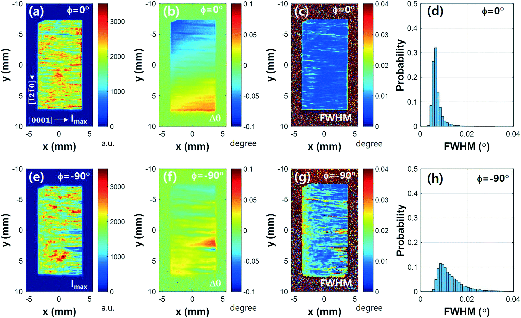 | ||
| Fig. 2 Images reconstructed from partially diffracted images at two different azimuthal angles. Maximum intensity, bending-angle and FWHM at ϕ = 0° and −90° are described in (a and e), (b and f) and (c and g), respectively. Stripe patterns are shown in all figures. Anisotropic bending-angles and FWHM were observed. Histograms of the FWHM map of (c) and (g) are described in (d) and (h), respectively. | ||
In the case of ϕ = −90°, the image reconstructed from the peak intensity in Fig. 2(e) showed stripe patterns similar to those in Fig. 2(a). However, the overall intensities over the film were smaller than ϕ = 0°. The lattice-plane orientation map in Fig. 2(f) showed different features compared with the lattice-plane orientation map ϕ = 0°. Here, the rotation axis of θ angle was parallel to [0001] and perpendicular to [20]. Unlike Fig. 2(b), stripe patterns with bending-angle modulation and undulation were observed. At this azimuthal angle, we rotated θ with respect to the [0001] axis, such that the bending-angle difference from the top and bottom of the image indicates film bending rather than twisting or torsion. The irregular stripe patterns in this image indicates that stresses were relaxed with the formation of stripe patterns. In previous reports,16 it has been suggested that the anisotropic thermal expansion coefficient can generate wafer bending that releases stresses. Thus, the epitaxial layer twisting and torsion could generate stripe patterns in the [0001] direction. However, more suitable model of stress relaxation specialized for homo-epitaxial layer is in demand since there are no models for homo-epitaxial layers. The evaluated FWHM maps under these conditions had values larger than ϕ = 0°. The stripe patterns were more complex than those in Fig. 2(c) and became more pronounced owing to multi-domain features, where the FWHM distribution was 0.008 ± 0.002°, as described in Fig. 2(h).
Fig. 3(a) depicts the x, y-dependent bending distributions over the epitaxial layer by combining Δθ maps at ϕ = 0° and ϕ = −90°. The [0001] directions were mainly inclined in the x-directions. From the wafer edge (x, y) = (0, −7), the quivers inclined to +x-direction then gradually changed to the −x-direction as the y components increased, which also showed a sample twist. A line profile with a smaller sampling ratio is shown in the right side of Fig. 3(a). The change of the y-components was smaller than that of the x-components whereas the sign of the y-component changed frequently owing to the bending-angle modulation, which is related to strain relaxation. These results allowed us to interpret the twisting and modulations of the lattice-planes, which resulted in stripe patterns, as illustrated in the Fig. 3(b). This is because the doping concentration of Si was 1 × 1016 cm−3 that was low enough to transfer the substrate feature. Therefore, bending features exist in the GaN substrate and to the homo-epitaxial layer.
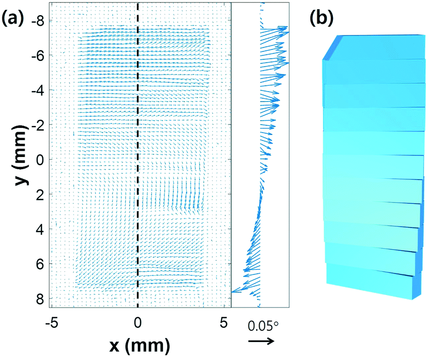 | ||
| Fig. 3 Vector plot of domain bending directions evaluated from Δθ at two different azimuthal angles are shown (a). Line profile along the dashed line in the left figure on the right side represents the twisted lattice. Lattice-plane twisting and stripe patterns parallel to [0001] direction over the epitaxial layer is shown (b). | ||
A bending-angle distribution function was obtained from Fig. 3 by changing the Cartesian coordinate into spherical coordinates, as shown in Fig. 4. A normal distribution function was used for this evaluation. The mean value was 0.030° and the half width at half maximum was 0.013°. This mean bending-angle was similar to the distribution of a previously reported 4-inch c-plane wafer,28 but larger than that of a 2-inch c-plane wafer.27 Our epitaxial layer is oriented in the m-plane, and we cannot directly compare the obtained distribution function with results for the c-plane; however, we believe that this value can be used to estimate the crystal quality quantitatively.
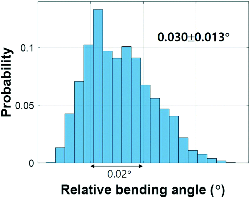 | ||
| Fig. 4 Bending-angle distribution evaluated from the polar angles over the wafer in Fig. 3. The distribution shows 0.030° ± 0.013°. | ||
Fig. 5 shows the high-resolution X-ray rocking curves of the m-plane GaN (100) at various positions for two different azimuthal angles. Although these results are consistent with Fig. 2(f), the details are limited by the dynamic range of the FPS detector. The X-ray rocking curve results at ϕ = 0° are shown in Fig. 5(a). The legend indicates the (x, y) coordinates in the wafer, as for previous figures. The figures show narrow and sharp peaks, representative of high-quality single domains. The values are in the 12 to 16 arcsec range. When we rotated the sample from ϕ = 0° to −90°, the X-ray rocking curve profiles showed multiple domain structures. These complex structures are related with the bending-angle modulation in the y-direction, as shown in Fig. 3. The frequent change of sign suggests that the bending direction can remarkably enhance the broadening of the mosaicity.
 | ||
| Fig. 5 High resolution X-ray diffraction profiles at various points in the epitaxial film. Sharper single peaks at ϕ = 0° (a), and broader and more complex peaks, which represent multi-domain structures (b). The legends are x, y positions in the wafer coordinates. | ||
Stripe patterns in nonpolar GaN surfaces are strongly related with anisotropic diffusion directions. In the case of an m-plane GaN, the diffusion barrier parallel to the [0001] direction for migration of Ga and N adatoms was 0.93 eV.30 Conversely, the diffusion barrier perpendicular to the [0001] direction was calculated to be 0.21 eV. The corresponding diffusion lengths in the [0001] direction evaluated from the diffusion barrier were only 1.5 and 5.1% at 1000 K and 1400 K, respectively. From these results, we expect that the stripe patterns should be perpendicular to [0001] direction, which is unlike our previous findings. However, our results in Fig. 2 and 3 cannot be explained by previous reports.30 In the case of the a-plane, the diffusion barrier parallel to the [0001] direction was smaller than that in the perpendicular direction of [0001].30 Thus, the stripe patterns should be parallel to [0001]. Our free-standing m-GaN was cut from a thick c-plane GaN (thicker than 7.5 mm) and then sliced to the m-plane GaN. Because the maximum wafer size of nonpolar GaN depends on the bulk GaN thickness it is hard to produce large nonpolar GaN substrates. Therefore, these stripe patterns parallel to c-direction might be threading dislocations created in the bulk GaN boule.
Another possible explanation is film cracking caused by the anisotropic thermal expansion coefficient.16 Once strain is generated in the film, the film undergoes a plastic deformation to reduce internal strain. Twisting the film along the [20] direction can relax the strain by generating cracks parallel to [0001] direction. Although the origin of anisotropic behavior is controversial, our findings based on X-ray diffraction topography at two different azimuthal angles will be helpful for improving the overall quality of epitaxial layers.
We expect that the anisotropic mosaicity will influence the electrical properties. According to K. H. Baik et al.,31 an a-plane GaN LED on sapphire substrate shows electrical anisotropy and the electrical property is affected by basal plane stacking faults (BSF). The sheet resistance parallel to the c-axis was higher than m-axis explained by carrier scattering of BSF. Although we did not get the electrical properties in the current experiment, we believe that the results will be similar with their results.
4 Conclusion
In conclusion, we have observed anisotropic mosaicity of a m-plane GaN by X-ray diffraction topography images and X-ray rocking curve analysis. Reconstructed images from the peak intensity showed striped patterns along the [0001] direction. A lattice-plane orientation map calculated from the peak position of the rocking curve images showed that the lattice planes were twisted along the [20] direction and bending-angle modulation along this direction. The evaluated bending-angle distribution was 0.030 ± 0.013°. X-ray rocking curve profiles at ϕ = 0° showed sharp single domain features with low mosaicity. At ϕ = −90° the X-ray rocking curve profile showed multi-domains with high mosaicity. We propose that threading dislocations in the [0001] direction, formed during bulk GaN growth or anisotropic thermal expansion, could cause of this anisotropic feature. Our new findings will be useful for controlling the growth of high quality m-plane GaN epitaxial layers.
Conflicts of interest
There are no conflicts of interest to declare.Acknowledgements
The measurements were performed at the NIMS beamline BL15XU under proposal No. 2018B4505 and at the Japan Synchrotron Radiation Research Institute BL20B2 under proposal No. 2018B1010, SPring-8. This work was supported by the Ministry of Education, Culture, Sports, Science and Technology (MEXT) “Program for Research and Development of Next-Generation Semiconductor to Realize Energy-Saving Society” and Basic Science Research Program through the National Research Foundation of Korea (NRF) funded by the Ministry of Education (2018R1A6A3A03012052). We thank Andrew Jackson, PhD, from Edanz Group (http://www.edanzediting.com/ac) for editing a draft of this manuscript.References
- H. Amano, M. Kito, K. Hiramatsu and I. Akasaki, Jpn. J. Appl. Phys., 1989, 28, L2112–L2114 CrossRef CAS.
- S. Nakamura, T. Mukai, M. Senoh and N. Iwasa, Jpn. J. Appl. Phys., 1992, 31, L139–L142 CrossRef CAS.
- Y. Wu, D. Kapolnek, J. P. Ibbetson, P. Parikh, B. P. Keller and U. K. Mishra, IEEE Trans. Electron Devices, 2001, 48, 586–590 CrossRef CAS.
- W. Saito, Y. Takada, M. Kuraguchi, K. Tsuda, I. Omura, T. Ogura and H. Ohashi, IEEE Trans. Electron Devices, 2003, 50, 2528–2531 CrossRef CAS.
- T. Palacios, A. Chakraborty, S. Heikman, S. Keller, S. P. DenBaars and U. K. Mishra, IEEE Electron Device Lett., 2006, 27, 13–15 CAS.
- F. Bernadini, V. Fiorentini and D. Vanderbilt, Phys. Rev. B: Condens. Matter Mater. Phys., 1997, 56, R10024–R10027 CrossRef.
- V. Fiorentini, F. Bernardini, F. D. Sala, A. D. Carlo and P. Lugli, Phys. Rev. B: Condens. Matter Mater. Phys., 1999, 60, 8849–8858 CrossRef CAS.
- T. Takeuchi, H. Takeuchi, S. Sota, H. Sakai, H. Amano and I. Akasaki, Jpn. J. Appl. Phys., 1997, 36, L177–L179 CrossRef CAS.
- J. S. Im, H. Kollmer, J. Off, A. Sohmer, F. Scholz and A. Hangleiter, Phys. Rev. B: Condens. Matter Mater. Phys., 1998, 57, R9435–R9438 CrossRef.
- R. Langer, J. Simon, V. Ortiz, N. T. Pelekanos, A. Barski, R. André and M. Godlewski, Appl. Phys. Lett., 1999, 74, 3827–3829 CrossRef CAS.
- R. Cingolani, A. Botchkarev, H. Tang, H. Morkoç, G. Traetta, G. Coli, M. Lomascolo, A. Di Carlo, F. Della Sala and P. Lugli, Phys. Rev. B: Condens. Matter Mater. Phys., 2000, 61, 2711–2715 CrossRef CAS.
- P. Lefebvre, A. Morel, M. Gallart, T. Taliercio, J. Allègre, B. Gil, H. Mathieu, B. Damilano, N. Grandjean and J. Massies, Appl. Phys. Lett., 2001, 78, 1252–1254 CrossRef CAS.
- M. D. Craven, S. H. Lim, F. Wu, J. S. Speck and S. P. DenBaars, Appl. Phys. Lett., 2002, 81, 469–471 CrossRef CAS.
- C. Q. Chen, M. E. Gaevski, W. H. Sun, E. Kuokstis, J. P. Zhang, R. S. Q. Fareed, H. M. Wang, J. W. Yang, G. Simin, M. A. Khan, H. Maruska, D. W. Hill, M. M. C. Chou and B. Chai, Appl. Phys. Lett., 2002, 81, 3194–3196 CrossRef CAS.
- H. Wang, C. Chen, Z. Gong, J. Zhang, M. Gaevski, M. Su, J. Yang and M. A. Khan, Appl. Phys. Lett., 2004, 84, 499–501 CrossRef CAS.
- C. Roder, S. Einfeldt, S. Figge, T. Paskova, D. Hommel, P. P. Paskov, B. Monemar, U. Behn, B. A. Haskell, P. T. Fini and S. Nakamura, J. Appl. Phys., 2006, 100, 103511 CrossRef.
- Q. Sun, S. Y. Kwon, Z. Ren, J. Han, T. Onuma, S. F. Chichibu and S. Wang, Appl. Phys. Lett., 2008, 92, 051112 CrossRef.
- B. Liu, R. Zhang, Z. L. Xie, J. Y. Kong, J. Yao, Q. J. Liu, Z. Zhang, D. Y. Fu, X. Q. Xiu, P. Chen, P. Han, Y. Shi, Y. D. Zheng, S. M. Zhou and G. Edwards, Appl. Phys. Lett., 2008, 92, 261906 CrossRef.
- M. A. Moram, C. F. Johnston, J. L. Hollander, M. J. Kappers and C. J. Humphreys, J. Appl. Phys., 2009, 105, 113501 CrossRef.
- W. Berg, Naturwissenschaften, 1931, 19, 391 CrossRef CAS.
- R. W. Armstrong and J. M. Schultz, Surf. Sci., 1968, 12, 19 CrossRef CAS.
- S. Kikuta, K. Kohra and Y. Sugita, Jpn. J. Appl. Phys., 1966, 5, 1047–1055 CrossRef CAS.
- T. Ishikawa, T. Kitano and J. Matui, J. Appl. Crystallogr., 1987, 20, 344–348 CrossRef CAS.
- C. Ferrari, D. Korytar and J. Kumar, Il Nuovo Cimento D, 1997, 19, 165–173 CrossRef.
- A. T. Macrander, S. Krasnicki, Y. Zhong, J. Maj and Y. S. Chu, Appl. Phys. Lett., 2005, 87, 194113 CrossRef.
- J. Guo, Y. Yang, B. Raghothamachar, M. Dudley and S. Stoupin, J. Electron. Mater., 2018, 47, 903–909 CrossRef CAS.
- J. Kim, O. Seo, C. Song, S. Hiroi, Y. Chen, Y. Irokawa, T. Nabatame, Y. Koide and O. Sakata, Appl. Phys. Express, 2018, 11, 081002 CrossRef.
- J. Kim, O. Seo, C. Song, Y. Chen, S. Hiroi, Y. Irokawa, T. Nabatame, Y. Koide and O. Sakata, CrystEngComm, 2018, 20, 7761–7765 RSC.
- J. Kim, O. Seo, C. Song, Y. Chen, S. Hiroi, Y. Irokawa, T. Nabatame, Y. Koide and O. Sakata, CrystEngComm, 2019, 14, 2247–2466 Search PubMed.
- L. Lymperakis and J. Neugebauer, Phys. Rev. B: Condens. Matter Mater. Phys., 2009, 79, 241308(R) CrossRef.
- K. H. Baik, Y. G. Seo, S. Song, S. Lee, J. Kim, J. Son and S. Hwang, IEEE Photonics Technol. Lett., 2010, 22, 595–597 CAS.
| This journal is © The Royal Society of Chemistry 2019 |