
 Open Access Article
 This Open Access Article is licensed under a Creative Commons Attribution-Non Commercial 3.0 Unported Licence
Lattice-plane bending angle modulation of Mg-doped GaN homoepitaxial layer observed by X-ray diffraction topography
Jaemyung
Kim
ab,
Okkyun
Seo
abc,
Chulho
Song†
 b,
Satoshi
Hiroi
bc,
Yanna
Chen
bc,
Yoshihiro
Irokawa
a,
Toshihide
Nabatame
a,
Yasuo
Koide
a and
Osami
Sakata
*abc
b,
Satoshi
Hiroi
bc,
Yanna
Chen
bc,
Yoshihiro
Irokawa
a,
Toshihide
Nabatame
a,
Yasuo
Koide
a and
Osami
Sakata
*abc
aCenter for GaN Characterization, Research Network and Facility Services Division (RNFS), National Institute for Materials Science (NIMS), Tsukuba, Ibaraki, 305-0047 Japan. E-mail: SAKATA.Osami@nims.go.jp
bSynchrotron X-ray Group, Research Center for Advanced Measurement and Characterization, NIMS, Kouto, Sayo, Hyogo, 679-5148 Japan
cSynchrotron X-ray Station at SPring-8, RNFS, NIMS, Kouto, Sayo, Hyogo, 679-5148 Japan
First published on 11th March 2019
Abstract
We have studied the lattice-plane modulation of Mg-doped GaN homoepitaxial layers by X-ray diffraction topography. X-ray rocking curve images and full-width at half maxima images of a 2 inch GaN wafer were obtained by an image stacking method. Low frequency components evaluated from Fourier transformations of the X-ray rocking curves tended to increase as the Mg-doping concentration increased, which indicates an increase of film lattice modulation. For Mg-dopant concentrations greater than 1019 cm−3, the film lattice-plane changed from a convex to concave shape and became wrinkled. We attribute this lattice-plane modulation to the relaxation of strain in the in-plane direction after the generation of dislocations by Mg doping.
Introduction
A recently developed hydride vapour phase epitaxy (HVPE) method has enabled the growth of large and high-quality GaN wafers.1,2 Homo-epitaxial layers grown on this GaN substrate show the highest crystallinity available in industry.3,4 However, for applications to optoelectronics5,6 and power devices,7,8 control of the dopant concentration is a critical factor. After electron beam irradiation and thermal annealing, Mg-doped GaN shows a considerable increase of photoluminescence (PL) efficiency.5,6 Although a Mg and hydrogen assisted model has been proposed to explain the increase of the PL efficiency, the actual mechanism of the increase remains a topic of debate.9 Mg-Doping to GaN increases the lattice parameters in both the a and c directions, but the lattice constant variations are very small.10 In the case of Si-doped GaN, sometimes, it shows strain, dislocations, and even cracks in its films, which deteriorate the GaN crystal quality.11 However, the microscale information obtained to date is not appropriate for understanding how these effects influence the overall wafer on a macroscopic scale such as HRTEM (high-resolution transmission electron microscopy)12 or EELS (electron energy loss spectroscopy).13 A better understanding of the wafer scale origins is needed to overcome these side effects and enable mass production of GaN wafers.Although X-ray rocking curves are widely used to observe GaN crystallinity, this technique only gives local rather than global information. Thus, conventional rocking curve measurements are not suitable for evaluating the crystallinity of the whole wafer. To overcome this issue, X-ray rocking curves have been combined with scanning methods based on motorized sample stages.1,14 However, these approaches do not fully cover the whole wafer owing to time and cost limitations.
In the case of an X-ray diffraction topography technique based on the Berg–Barrett method,15–21 it has provided us with wafer scale information such as the dislocation distribution. This method is suitable for crystalline materials rather than layered materials because 2D materials have Bragg rods instead of Bragg points in the reciprocal space.22 Recently developed lattice-plane orientation mapping shows the importance of wafer scale imaging for understanding wafer bending and crystallinity distribution over 2 and 4 inch GaN wafers.20,21
Here we show the effects of Mg doping on GaN homoepitaxial layers over a wafer by X-ray diffraction topography methods. We applied Fourier analysis of the bending angle line profiles to reveal an increase of the bending angle modulation as the Mg concentration increased owing to strain relaxation in the in-plane directions.
Experimental details
The samples were 2 μm-thick Mg-doped GaN layers with Mg-dopant concentrations of 1017, 1018, and 1019 cm−3 grown on a 1 μm-thick undoped GaN layer on a 330 μm-thick GaN (0001) 2 inch wafer as the substrate. The concentrations of Mg in the GaN layers were estimated using a calibration curve of Mg dopant concentrations, which were obtained from analysis of secondary ion mass spectroscopy depth profiles of reference samples, as a function of Cp2Mg (bis cyclopentadienyl magnesium) supply amounts, and had a standard deviation of 10%. The X-ray diffraction topography experiments were performed at BL20B2 SPring-8, Japan. An X-ray wavelength of 1.284 Å was selected with a Si (111) double crystal monochromator having a size of 100 mm (h) × 1.5 mm (v), which was large enough to fully cover the 2 inch wafer. A flat panel detector (C7942, Hamamatsu Photonics) with a pixel size of 50 × 50 μm2 was installed for image acquisition. The incident angle was adjusted to be 0.58°, which satisfied the GaN (11![[2 with combining macron]](https://www.rsc.org/images/entities/char_0032_0304.gif) 4) Bragg condition. We obtained partially diffracted images at various incident angles and evaluated the rocking curve images by an image stacking technique.20,21 In the case of a bent crystal, the positions that satisfied the Bragg condition diffracted X-rays. Six of the available diffraction configurations in the bent crystal are illustrated in Fig. 1(a)–(f). For a convex shape, the diffraction position moved to the right, when irradiated with X-rays from right to the left, as shown in Fig. 1(b). Conversely, if we increased the incident angle, the diffraction position moved to the left, as shown in Fig. 1(c). If the lattice-plane has a concave shape, the situation was reversed, as shown in Fig. 1(d)–(f). Through this X-ray diffraction technique, we obtained bending angle information on the lattice-plane.
4) Bragg condition. We obtained partially diffracted images at various incident angles and evaluated the rocking curve images by an image stacking technique.20,21 In the case of a bent crystal, the positions that satisfied the Bragg condition diffracted X-rays. Six of the available diffraction configurations in the bent crystal are illustrated in Fig. 1(a)–(f). For a convex shape, the diffraction position moved to the right, when irradiated with X-rays from right to the left, as shown in Fig. 1(b). Conversely, if we increased the incident angle, the diffraction position moved to the left, as shown in Fig. 1(c). If the lattice-plane has a concave shape, the situation was reversed, as shown in Fig. 1(d)–(f). Through this X-ray diffraction technique, we obtained bending angle information on the lattice-plane.
 | ||
| Fig. 1 X-ray diffraction configurations in concave (a–c) and convex (d–f) lattice-planes illustrated at various incident angles. The diffracted X-rays are those emitted from lattice-planes that satisfy the Bragg condition. | ||
Results and discussion
The bending angle maps at Mg concentrations of 1017, 1018, and 1019 cm−3 are shown in Fig. 2(a)–(c), respectively. The intensity patterns indicate the bending angles evaluated from the rocking curves at the respective detector pixel position. At Mg concentrations of 1017 and 1018 cm−3, the bending angle changed monotonously. However, at 1019 cm−3, modulation of the bending angles in the vicinity of the central parts was clearly seen. The overall bending angle envelope changed from a concave to convex shape. Both the envelope changes of the bending angles and film wrinkling are shown by the changes of the bending angle envelopes [Fig. 2(c)]. To understand the change of the bending angle quantitatively, we selected specific line profiles of each wafer, as shown in Fig. 2(d)–(f). The bending angles obtained from the upper sides of each wafer are shown in Fig. 2(d). For Mg concentrations of 1017 and 1018 cm−3, the overall values were shifted by ±0.05°. However, in the case of the highest doping concentration of 1019 cm−3, abrupt increases and decreases of the bending angles were observed, which implies the existence of lattice-plane modulation at high Mg concentrations. This situation was similar for the center and lower parts of the samples, as shown in Fig. 2(e) and (h). To determine the frequency components from the bending angle modulation, we applied Fourier transformations to the obtained line profiles. The calculated frequency components of the upper, middle, and lower parts are shown in Fig. 2(g)–(i), respectively. In the case of the upper region, the increase of the low frequency components strongly affected the bending angle fluctuation, as shown in Fig. 2(g). In the case of a Mg-doping concentration of 1019 cm−3, the dominant frequency was 0.67 × 10⁻⁶ Å−1 with a corresponding modulation period of approximately 9.4 mm. Another strong frequency component at 0.13 × 10⁻⁶ Å−1 with a 4.7 mm modulation period was also observed. These two strong frequency components mainly contributed to the wafer bending and wrinkling of the GaN films. | ||
| Fig. 2 Merged 2 inch GaN images at various Mg doping concentrations are illustrated in (a)–(c). The intensities in the image represent the bending angles evaluated from the partially diffracted X-ray images at respective pixel positions. Line profiles representing the wafer bending at the top, center, and lower parts are shown in (d)–(f). Fourier transformation results of these line profiles are shown in (g), (h), and (i), respectively. Low frequency components related to the lattice modulation dominate at an Mg concentration of 1019 cm−3. | ||
To understand the relationship between the amplitude obtained from Fourier transformation and the Mg concentration, we calculated the amplitude summation of Fig. 2(g–i), which can be used to represent the film modulation, as shown in Fig. 3(a). As the Mg concentration increased, the total amplitude increased. The trend was similar for the wafer upper, center, and lower parts. The mean values at a Mg-doping concentration of 1019 cm−3 were approximately two times as high as those at 1017 cm−3. We interpret this result as indicating that the high Mg doping of the GaN homoepitaxial layers increased the stress in the in-plane direction of the film. As shown in Fig. 3(b), the films had low bending at the initial stage. As the Mg concentration increased, the lattice-plane bending angle increased. At Mg concentrations greater than 1019 cm−3, the increase of stress enabled relaxation by film wrinkling. According to a report on stress relaxation18 of Si-doped GaN observed by Raman spectroscopy,11,24 an increase of the Si doping concentration induces stress relaxation of the films and the dislocation density increases. In this respect, our observation is similar to the previous report, which was based on a Si dopant.11 To confirm our model proposed in Fig. 3(b), we evaluated the full-width at half maxima (FWHM) maps by an image stacking method, as illustrated in Fig. 4(a)–(c). The color scale indicates the FWHM angle. For a Mg concentration of 1017 cm−3, the FWHM showed a homogeneous distribution. For a Mg concentration of 1018 cm−3, we observed an increase of the FWHM in the middle of the wafer. At a Mg concentration of 1019 cm−3, the edge parts inside the circles showed a particularly large FWHM, which indicated an increase of the mosaicity of GaN (114) domains. The increase of the FWHM in the vicinity of the wafer edge in Fig. 4(c) is the result of compressive stress relaxation in the in-plane direction if the substrates used have similar lattice-plane bending distributions. The origin of a small point-like area, having a large FWHM value within the circle in Fig. 4(c), cannot be explained without stress relaxation. This assumption is consistent with a previously mentioned report.23 The increase of FWHM is related to an increase of mosaicity or dislocation density.
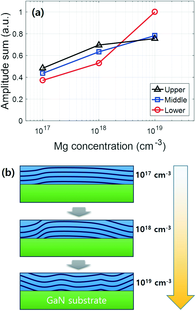 | ||
| Fig. 3 Amplitude summation evaluated from Fourier transformation is represented in (a). The evaluated values were proportional to the Mg concentration. The proposed Mg-induced lattice bending model is shown in (b). As the Mg dopant concentration increased, the lattice bending angle increased up to a Mg concentration of 1018 cm−3. At higher concentrations, the films became wrinkled and changed from a convex to concave shape. | ||
 | ||
| Fig. 4 FWHM maps of Mg concentrations of 1017 (a), 1018 (b), and 1019 cm−3 (c) evaluated from the image stacking method are described. As the Mg concentration increased, the FWHM increased owing to the increase of mosaicity induced by Mg atoms. The dashed circle area indicates a region of high mosaicity. | ||
According to previous reports, the dislocation density can be directly calculated from the rocking curve width broadening and the length of the Burgers vector.25,26 For the rocking curve obtained at the GaN (114) peak, the broadening provides the threading dislocation (TD) density. However, the best way to observe dislocations is to use transmission electron microscopy (TEM) with atomic resolution27 or atomic force microscopy (AFM) of a clean surface.29,30 Without measurements at this resolution, it is difficult to evaluate the dislocation density and the length of the Burgers vector. A recently developed two-photon excitation photoluminescence technique28 has also shown dislocation images in 3D. However, the spatial resolution of this method is insufficient to distinguish dislocations smaller than 300 nm. In some cases, a formula developed by Kaganer26 is useful for estimating the dislocation density. However, according to Barchuk et al., X-ray rocking curves can show the same features even at very different dislocation densities.31 They interpreted the broadening of rocking curves through wafer bowing and misorientation from a macroscopic viewpoint. From a microstructural point of view, they associated the rocking curve broadening with the dislocation density. They revealed that dislocation densities obtained from Monte Carlo simulations were strongly dependent on the model even with the same rocking curve. For these reasons, careful attention should be paid to interpreting dislocation densities based on X-ray rocking curves.
Conclusions
In conclusion, we have observed the lattice-plane bending angle modulations of GaN homoepitaxial layers by X-ray diffraction topography. As the Mg concentration increased, the bending angles increased and the film became wrinkled. At an Mg concentration of 1019 cm−3, the envelope of the lattice-plane changed from a concave to convex shape. Fourier transformations of the bending angle line profiles obtained from X-ray diffraction topography images showed an increase of low frequency components as the doping concentration increased. The evaluated low frequency components with periods of 9.4 and 4.7 mm was dominant under the highest doping concentration. The envelope of the overall lattice-planes became convex and wrinkled at high Mg concentrations. The increase of the FWHM at the wafer edge implies that stress relaxation occurs with an increase of dislocation density at high Mg concentrations.Conflicts of interest
There are no conflicts to declare.Acknowledgements
The measurements were performed at SPring-8 under proposals No. 2016B1028, 2017A1030, 2017B1029, 2017B1030, 2018B1010, 2017B4505, and 2018B4505. This work was supported by the Ministry of Education, Culture, Sports, Science and Technology (MEXT) “Program for Research and Development of Next-Generation Semiconductor to Realize Energy-Saving Society”. We thank Andrew Jackson, PhD, from Edanz Group (www.edanzediting.com/ac) for editing a draft of this manuscript.Notes and references
- R. Dwiliński, R. Doradziński, J. Garczyński, L. P. Sierzputowski, A. Puchalski, Y. Kanbara, K. Yagi, H. Minakuchi and H. Hayashi, J. Cryst. Growth, 2008, 310, 3911–3916 CrossRef.
- K. Fujito, S. Kubo, H. Nagaoka, T. Mochizuki, H. Namita and S. Nagao, J. Cryst. Growth, 2009, 311, 3011–3014 CrossRef CAS.
- M. Lee, D. Mikulik, M. Yang and S. Park, CrystEngComm, 2017, 19, 2036–2041 RSC.
- T. Kimura, K. Horibuchi, K. Kataoka and D. Nakamura, J. Cryst. Growth, 2018, 494, 17–25 CrossRef CAS.
- S. Nakamura, T. Mukai, M. Senoh and N. Iwasa, Jpn. J. Appl. Phys., 1992, 31, L139–L142 CrossRef CAS.
- H. Amano, M. Kito, K. Hiramatsu and I. Akasaki, Jpn. J. Appl. Phys., 1989, 28, L2112–L2114 CrossRef CAS.
- Y. Wu, D. Kapolnek, J. P. Ibbetson, P. Parikh, B. P. Keller and U. K. Mishra, IEEE Trans. Electron Devices, 2001, 48, 586–590 CrossRef CAS.
- W. Saito, Y. Takada, M. Kuraguchi, K. Tsuda, I. Omura, T. Ogura and H. Ohashi, IEEE Trans. Electron Devices, 2003, 2528–2531 CrossRef CAS.
- J. L. Lyons, A. Janotti and C. G. Van de Walle, Phys. Rev. Lett., 2012, 108, 156403 CrossRef PubMed.
- P. Prystawko, M. Leszczynski, B. Beaumont, P. Gibart, E. Frayssinet, W. Knap, P. Wisniewski, M. Bockowski, T. Suski and S. Porowski, Phys. Status Solidi B, 1998, 210, 437–443 CrossRef CAS.
- L. T. Romano, C. G. Van de Walle, J. W. Ager, W. Götz and R. S. Kern, J. Appl. Phys., 2000, 87, 7745–7752 CrossRef CAS.
- S. D. Lester, F. A. Ponce, M. G. Craford and D. A. Steigerwald, Appl. Phys. Lett., 1995, 66, 1249–1251 CrossRef CAS.
- I. Arslan and N. D. Browning, Phys. Rev. Lett., 2003, 91, 165501 CrossRef CAS PubMed.
- Y. Cui, X. Hu, X. Xie, R. Wang and X. Xu, CrystEngComm, 2017, 19, 3844–3849 RSC.
- J. Chaudhuri, M. H. Ng, D. D. Koleske, A. E. Wickenden and R. L. Henry, Mater. Sci. Eng., B, 1999, 64, 99–106 CrossRef.
- X. Xu, R. P. Vaudo, C. Loria, A. Salant, G. R. Brandes and J. Chaudhuri, J. Cryst. Growth, 2002, 246, 223–229 CrossRef CAS.
- B. Raghothamachar, G. Dhanaraj, J. Bai and M. Dudley, Microsc. Res. Tech., 2006, 69, 343–358 CrossRef CAS PubMed.
- K. Barla, G. Bomchil, R. Herino, J. C. Pfister and J. Baruchel, J. Cryst. Growth, 1984, 68, 721–726 CrossRef CAS.
- D. Lübbert, C. Ferrari, P. Mikulík, P. Pernot, L. Helfen, N. Verdi, D. Korytár and T. Baumbach, J. Appl. Crystallogr., 2005, 38, 91–96 CrossRef.
- J. Kim, O. Seo, C. Song, S. Hiroi, Y. Chen, Y. Irokawa, T. Nabatame, Y. Koide and O. Sakata, Appl. Phys. Express, 2018, 11, 081002 CrossRef.
- J. Kim, O. Seo, C. Song, Y. Chen, S. Hiroi, Y. Irokawa, T. Nabatame, Y. Koide and O. Sakata, CrystEngComm, 2018, 20, 7761–7765 RSC.
- J. Als-Nielsen and D. McMorrow, Elements of Modern X-Ray Physics, New York, 2001 Search PubMed.
- C. Kisielowski, J. Krüger, S. Ruvimov, T. Suski, J. W. Ager, E. Jones, Z. Liliental-Weber, M. Rubin, E. R. Weber, M. D. Bremser and R. F. Davis, Phys. Rev. B: Condens. Matter Mater. Phys., 1996, 54, 17745–17753 CrossRef CAS.
- I. Lee, I. Choi, C. Lee, E. Shin, D. Kim, S. Noh, S. Son, K. Lim and H. Lee, J. Appl. Phys., 1998, 83, 5787–5791 CrossRef CAS.
- B. Heying, X. H. Wu, S. Keller, Y. Li, D. Kapolnek, B. P. Keller, S. P. DenBaars and J. S. Speck, Appl. Phys. Lett., 1996, 68, 643–645 CrossRef CAS.
- V. M. Kaganer, O. Brandt, A. Trampert and K. H. Ploog, Phys. Rev. B: Condens. Matter Mater. Phys., 2005, 72, 045423 CrossRef.
- C. Chen, C. Zhu, E. R. White, C. Chiu, M. C. Scott, B. C. Regan, L. D. Marks, Y. Huang and J. Miao, Nature, 2013, 496, 74–77 CrossRef CAS PubMed.
- T. Tanikawa, K. Ohnishi, M. Kanoh, T. Mukai and T. Matsuoka, Appl. Phys. Express, 2018, 11, 031004 CrossRef.
- A. M. Walker, B. Slater, J. D. Gale and K. Wright, Nat. Mater., 2004, 3, 715–720 CrossRef CAS PubMed.
- S. Dumrul, S. Bazzana, J. Warzywoda, R. R. Biederman and A. Sacco Jr., Microporous Mesoporous Mater., 2002, 54, 79–88 CrossRef CAS.
- M. Barchuk, V. Holý and D. Rafaja, J. Appl. Phys., 2018, 123, 161552 CrossRef.
Footnote |
| † Current address: NISSAN ARC, LTD., 1 Natsushima-cho, Yokosuka, Kanagawa, 237-0061 Japan. |
| This journal is © The Royal Society of Chemistry 2019 |