DOI:
10.1039/C8CE01863D
(Paper)
CrystEngComm, 2019,
21, 1718-1727
Facile synthesis of Ag2Te nanowires and thermoelectric properties of Ag2Te polycrystals sintered by spark plasma sintering
Received
31st October 2018
, Accepted 22nd December 2018
First published on 26th December 2018
Abstract
Ag2Te nanowires with a diameter of approximately 200 nm and a length of several micrometers were prepared using a simple one-step solvothermal method without templates and surfactants. Ag(NO)3 and Na2TeO3 were used as the Ag and Te sources, respectively, and N2H4·H2O was used as the reducing agent. Based on the study of the morphology and composition of the Ag2Te nanowires obtained under different hydrothermal conditions, a possible formation mechanism of Ag2Te nanowires was proposed. An Ag-rich Ag2Te sample was prepared by adjusting the molar ratio of Ag and Te. Furthermore, Ag2Te nanowire powders were condensed to bulk materials by spark plasma sintering at 673 K for 5 min. The thermoelectric properties of the Ag2Te bulk materials were measured between 323 K and 673 K. The phase transition temperature of the transformation from α-Ag2Te to β-Ag2Te was determined to be 419 K by differential scanning calorimetry. The highest ZT values of pure Ag2Te and Ag self-doped Ag2Te bulk samples reached 0.9 and 1.1 at 623 K, respectively. These results indicate that this one-pot technique for preparing the Ag self-doped Ag2Te sample with enhanced thermoelectric performance may be widely used in other thermoelectric systems that can be fabricated by solution methods.
Introduction
Thermoelectric (TE) power generation has been considered to be a viable solution for improving the energy efficiency of heat engines through the conversion of waste heat into electricity. However, in order for TE power generation to become competitive with conventional energy conversion systems, materials with high performance are needed, as evaluated by the dimensionless thermoelectric figure of merit ZT, ZT = σS2T/κ, where σ, κ, S, and T are the electrical conductivity, thermal conductivity, Seebeck coefficient, and absolute temperature, respectively. T is the average temperature between the hot and cold sides.1,2 A high ZT requires the simultaneous presence of a large Seebeck coefficient, a high electrical conductivity, and a low thermal conductivity in a material; the realization of this combination of properties has been a long-standing challenge due to the fundamental relationships among these parameters.3
Generally, the performance of thermoelectric materials can be optimized by approaches such as doping, nanostructuring, and morphology control. For example, in recent reports, Liu et al. enhanced the ZT value of CoSb3 to 0.1 by adding excess Sb during the synthetic process.4 He's group reported a new approach of incorporating PbSnS2 displacement layers in PbTe, resulting in a significant reduction in lattice thermal conductivity down to 0.8 W m1 K2, or almost 30% of that for bulk PbTe at room temperature.5 Furthermore, these researchers also presented experimental evidence and theoretical validation for the role of a ternary element (Na) in controlling the morphology of nanoscale PbS crystals nucleating in a PbTe matrix,6 providing a good basis for further optimization of the thermoelectric properties of this important bulk thermoelectric system by morphological control. Wu et al. reported that a high density of nanoscale grain boundaries dramatically lowered the thermal conductivity of PbS thermoelectric materials by effectively scattering long wavelength phonons.7 Tang's group achieved remarkably high thermoelectric performance ZT ∼ 1.7 at 873 K by the introduction of nanoscale phase separation in SnSe.8 Among the nanostructured materials, nanowires have been demonstrated to exhibit superior electrical, optical, mechanical, and thermal properties and can be used as fundamental building blocks for nanoscale science and technology.9–12 In this work, we seek to utilize spark plasma sintering (SPS) to densify Ag2Te nanowires into a bulk sample with good thermoelectric properties. To the best of our knowledge, there have been no thermoelectric-related reports on Ag2Te bulk materials prepared from Ag2Te nanowires.
Silver telluride (Ag2Te) is a narrow-band gap semiconductor (Eg ∼ 0.09 eV at room temperature) that has many unique properties for thermoelectric applications, such as (1) low thermal conductivity associated with the disordered structure of Ag atoms in the Ag2Te lattice due to the high mobility of Ag atoms,13,14 (2) a high power factor due to high electron mobility that is also observed in other silver chalcogenides,13,15,16 (3) tunable carrier density modulated by nonstoichiometric compositions of Ag2Te, in which the defects, including completely ionized silver atoms at interstitial sites and vacancies, can create donor and acceptor levels, respectively,17 and (4) low-temperature phase transition from the monoclinic phase to the cubic phase at approximately 419 K. According to previous reports, the maximum ZT of pristine Ag2Te reached 0.6 at 700 K.13,14,18–30 Through alloying with PbTe or Ag2Se, Ag2Te ZT can be promoted to 1 or 1.2, respectively.13,21 A number of methods for the synthesis of Ag2Te nanostructures have been explored. For example, Ag2Te nanowires were obtained by cathodic electrolysis from a dimethyl sulfoxide (DMSO) solution containing AgNO3 and TeCl4 in a porous anodic alumina membrane.21 Ag2Te nanotubes have been prepared by a solvothermal process without the use of a template or surfactant.22 A template-based method in which Te nanorods were used as template reagents has been developed for the synthesis of Ag2Te nanorods.23 However, most of these syntheses must use templates that serve as physical scaffolds or require complex processes and reagents. In this study, we demonstrated a simple chemical synthesis of Ag2Te nanowires without any templates or surfactants. Stoichiometric and Ag-rich Ag2Te nanowires were prepared by tuning the Ag/Te ratio during the synthesis process. A possible growth mechanism of the Ag2Te nanowires has been elucidated. The as-prepared Ag2Te nanowires and Ag–Ag2Te nanowires were sintered to bulk samples by SPS. Interestingly, both bulk samples are pure Ag2Te without any detected Ag phase. We supposed that the Ag phase in the Ag2Te nanowires was doped into the Ag2Te lattice during the SPS process. The thermoelectric properties of the bulk samples were measured from 300 K to 700 K, showing that enhanced ZT values of 0.9 and 1.1 at 630 K were achieved for the pristine Ag2Te bulk sample and the Ag self-doped Ag2Te sample, respectively.
Experimental section
All of the chemical reagents used in this work were of analytical grade; in a typical experiment, Na2TeO3 (0.5–0.55 mmol, 99.9%) and AgNO3 (1 mmol, 99.8%) were first added into deionized water (15 ml), and the mixture was stirred for 5 min. A large amount of light yellow suspended matter was produced in the solution. Then, hydrazine (0.4 ml, 80% by volume) and ammonium hydroxide (0.4 ml, 25–28% by volume) were added to the solution as the reducing reagent and buffer, respectively. The light yellow suspended matter turned black immediately upon the addition of hydrazine. The mixed solution was then transferred into a Teflon-lined stainless steel autoclave (100 ml capacity), sealed and maintained at 120–180 °C for 6–24 h. The resultant black solid product was filtered and washed with deionized water and ethanol, and then dried at 60 °C for 5 h in air. The precursor powders were charged into column graphite dies with an internal diameter of 15 mm and then were sintered in a vacuum using an SPS system (FDC SPS6321X, Japan) under 50 MPa at 773 K for 5 min. The sintered bulk samples are disks with a dimension of Φ15 mm. The initial raw material ratios of Ag and Te were set to 1![[thin space (1/6-em)]](https://www.rsc.org/images/entities/char_2009.gif) :1, 1:1.05 and 1:1.1. The samples were named A2Tx (x = 1, 1.05, 1.1) for different raw material ratios.
:1, 1:1.05 and 1:1.1. The samples were named A2Tx (x = 1, 1.05, 1.1) for different raw material ratios.
The phase structure was analyzed by X-ray diffraction (XRD, MiniFlex 600, Japan) with CuKα radiation. The morphology of the powders and the fractography of the bulk samples were observed by scanning electron microscopy (SEM, EVO18, Germany). The microstructure of the bulk was also examined using transmission electron microscopy (TEM, Philips Tecnai F20, Dutch). The TE properties were evaluated along the sample section perpendicular to the pressing direction of SPS. The Seebeck coefficient and electrical resistivity were measured from 323 K to 673 K in a helium atmosphere using a Seebeck coefficient/electrical resistance measuring system (ZEM-3, Ulvac-Riko, Japan). The density of the sample was measured by the Archimedes method. The thermal conductivity of the sample was obtained from the thermal diffusivity (D) measured by the laser flash method (NETZSCH, LFA457, Germany), specific heat capacity (Cp) and density (ρ). A differential scanning calorimeter (DSC, STA 449 F3, Germany) was operated under an argon atmosphere with a heating and cooling rate of 10 °C min−1.
Results and discussion
1. Powder characterization
Fig. 1 shows the XRD patterns of the silver telluride nanostructure powders obtained under different hydrothermal conditions (120 to 180 °C for 12 h (Fig. 1a), 140 °C for 6 to 24 h (Fig. 1b) and 140 °C for 0 to 45 min (Fig. 1c)). With varying hydrothermal temperature from 120 to 180 °C for a constant holding time of 12 h, the XRD patterns of all the powder samples are shown in Fig. 1(a), and it is observed that while all of the diffraction peaks match the monoclinic Ag2Te crystal structure (PDF #81-1985) [space group: P21/c (14)], there are still some different detectable phases, marked as Ag and Ag5Te3. With the increase in the reaction temperature to 140 °C, the Ag5Te3 impurity disappeared, but the diffraction peak of Ag became strong upon further increase in the temperature, as shown in Fig. 1(a). To synthesize the pure phase of Ag2Te, we fixed the hydrothermal temperature at 140 °C and tried different soaking times. As shown in Fig. 1(b), the main peaks are due to Ag2Te, but the Ag peaks are still observed for all the samples. To explore the growth mechanism of the Ag2Te nanowires, very short holding times (0 min, 15 min, 30 min, and 45 min) were used for synthesizing the samples. The XRD results obtained for these samples are shown in Fig. 1(c), and it is observed that when the holding time is fixed to 0 min and 15 min, the main phase of the sample is Ag, and with increasing reaction time, the intensities of the Ag2Te peaks increase, and the intensity of the Ag peak decreases. However, the Ag peak is still present in all the samples, which may be caused by the Te loss during the solution phase synthesis process. Therefore, an extra Te raw source was added into our subsequent syntheses in order to obtain the pure Ag2Te phase.
 |
| | Fig. 1 XRD patterns of the silver telluride nanostructure powders obtained under different hydrothermal conditions ((a) 120 to 180 °C for 12 h, (b) 140 °C for 6 to 24 h and (c) 140 °C for 0 to 45 min). | |
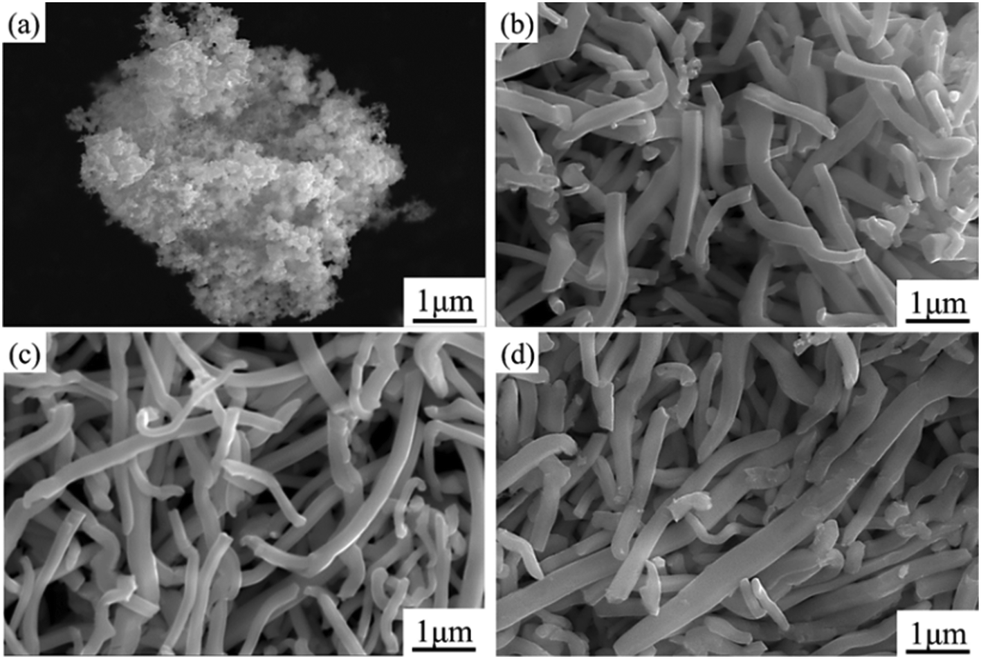
The morphology of the samples was observed by SEM. Fig. 2 shows the images of the powder samples prepared at 120 to 180 °C for 12 h, respectively. Fig. 3 shows the images of the as-synthesized samples prepared at 140 °C for different soaking times in the range of 0–24 h. As shown in Fig. 2(a), the nanowires synthesized at 120 °C are smaller with diameters of approximately 50 to 100 nm and a length of approximately one micrometer. Some flocculated nanoparticles and clumps are observed at the edge of the image, and the composition of the flocculated nanoparticles is identified to be 90% Ag and 10% Te using energy dispersive spectroscopy point scanning. As the temperature increases, the nanoparticles disappear and the nanowires generally become uniform and slender (Fig. 2(b)). As the temperature increases further, interconnected nanowires and dendrites appear at 160 °C and 180 °C, respectively (Fig. 2(c) and (d)). The edges of the nanowires disappear and fuse together to form irregular dendrites when the temperature increases to 180 °C. To the best of our knowledge, there are no reports in the literature on such morphologies of silver telluride. As observed in Fig. 3, the sample prepared with the time of 0 h is a pure Ag phase as observed from the XRD pattern of the 0 h sample presented in Fig. 1(c). The sample prepared for 12 h contains long and curved nanowires with a diameter of approximately 200 nm and a length of several micrometers. The nanowires became longer and wider after the soaking time was extended to 24 h. More interesting is the effect of the hydrothermal temperature on the morphology. The results in Fig. 2 and 3 show that temperature has a strong influence on the growth of Ag2Te nanowires. The pure phase of Ag2Te could not be synthesized by only adjusting the preparation time and temperature; therefore, we performed experiments with different initial raw material ratios. The initial raw material ratios were set to 1:1, 1:1.05 and 1:1.1. The samples were named A2Tx (x = 1, 1.05, 1.1) for different raw material ratios, and the hydrothermal conditions were 140 °C for 12 h.
 |
| | Fig. 2 SEM images of the as-synthesized samples at different temperatures of (a) 120 °C, (b) 140 °C, (c) 160 °C, and (d) 180 °C for 12 h. The inset of (a) is the quantitative element contents collected form the red circle area. | |
 |
| | Fig. 3 SEM images of the as-synthesized samples at 140 °C for different soaking times of (a) 0 h, (b) 6 h, (c) 12 h, and (d) 24 h. | |
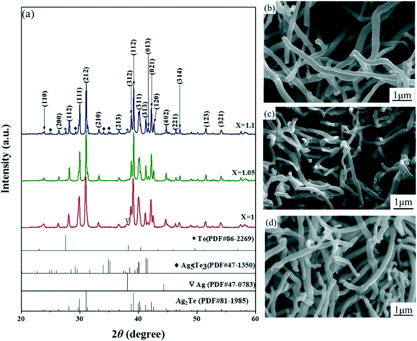
The XRD patterns and SEM images of the Ag2Te nanowires obtained using different initial raw material ratios and the TEM images of the A2T1.05 nanowires are shown in Fig. 4. It is observed from the SEM images that there is no significant difference in the morphology of the nanowires with different material ratios, implying that the raw material ratio has a negligible effect on the morphology. As observed from the XRD pattern shown in Fig. 4(a), an Ag impurity phase was detected when the raw material ratio was set to stoichiometric. Te and Ag5Te3 impurities were detected when the ratio was set at 2:1.1. The pure Ag2Te phase was synthesized under the conditions of 140 °C heat preservation for 12 h with a raw material ratio of 2:1.05.
 |
| | Fig. 4 (a) XRD patterns and SEM images of the as-synthesized samples with different initial material ratios ((b) x = 1.1, (c) x = 1.05 and (d) x = 1). | |
Fig. 5(a–d) show the morphologies of Ag2Te nanowires; the as-prepared Ag2Te is about 100 to 200 nm in diameter and several micrometers in length. The nanowires are crooked, and the surface of the nanowires is clear without amorphous layers. Fig. 5(e) is the SAED pattern of the Ag2Te nanowire shown in Fig. 5(a). Fig. 5(f) and (g) are the high resolution images of the Ag2Te nanowires shown in Fig. 5(b) and (c), respectively. The SAED and high resolution observations indicated that the as-prepared Ag2Te nanowires are single crystals and free of stacking faults. However, it's hard to confirm the crystal growth; this is in agreement with the crooked morphology of the nanowires. In Fig. 5(f), the different contrast on the edge and inside of the nanowires was considered to be caused by the different thicknesses of the nanowires.
 |
| | Fig. 5 TEM images of Ag2Te nanowires (a–d) and (e) SAED pattern from (a), (f) high resolution TEM image of the Ag2Te nanowire from (b) and (g) high resolution TEM image of the Ag2Te nanowire from (c). | |
2. Growth mechanism of Ag2Te nanowires
To study the chemical formation mechanism of Ag2Te nanowires, we characterized the samples with different reaction times by XRD. The obtained results are shown in Fig. 1(c). The powder obtained at the initial stage of the reaction is pure silver, and over time, silver telluride forms on the basis of the silver particles and the elemental silver is consumed to a certain extent, and then forms again in the solution for the further synthesis of silver telluride. Based on the XRD results and experimental phenomena, the chemical formation mechanism of the Ag2Te nanowires is proposed to occur via the following steps:| | | 2AgNO3 + Na2TeO3 = Ag2TeO3↓ + NaNO3 | (1) |
| | | Ag2TeO3 + N2H4 + 2H2O = 2Ag + 2NH3OH+ + TeO32− | (2) |
| | | 2NH3OH+ + N2H4 = 2NH4+ + N2↑ + 2H2O | (3) |
| | | 2TeO32− + 3N2H4 → 2TeX2− + 3N2↑ + 6H2O | (4) |
| | | TeX2− → (X − 1)Te + Te2− | (5) |
| | | 2Ag + Te = Ag2Te/2Ag+ + Te2− = Ag2Te | (6) |
At the beginning of the reaction, AgNO3 and Na2TeO3 are dissolved in deionized water after stirring and forming the Ag2TeO3 precipitate as described by eqn (1), as can be observed and confirmed by the yellowish precipitates produced in the early stages of the reaction. With the addition of N2H4, Ag2TeO3 is reduced by N2H4 to Ag atoms with the evolution of NH3OH+, and NH3OH+ is further reduced to NH4+ and N2 gas as described by eqn (2) and (3). This can be proved by the precipitates turning black after the addition of N2H4. The composition of the precipitates is determined to be Ag according to the XRD pattern shown in Fig. 1(c). Furthermore, eqn (3) can be confirmed by the observation with bubbling gas during the course of the reaction, and the measured pH value increases as the reaction proceeds. N2H4 reduces TeO32− to polytelluride ions TeX2− that consist of Te2− ions and Te atoms as described in eqn (4) and (5). Finally, the reduced Ag atoms and Ag+ ions that have not been reduced react with Te atoms and Te2− ions, respectively, and transform into Ag2Te as described in eqn (6). In this case, polytelluride ions TeX2− act as an active Te source here31 but the formation of polytelluride ions TeX2− is slow as confirmed by Li's report.32 Because of the higher chemical potential between the silver atoms and silver ions, the silver atoms are first reduced at the beginning of the reaction, and meanwhile, because the formation of the polytelluride ions TeX2− is slow, we could only observe the pure Ag phase in the XRD pattern at the beginning.
Based on the chemical formation mechanism, we further describe the possible morphological formation mechanism of Ag2Te nanowires, as shown in Fig. 6. The previously reported formation mechanisms of Ag2Te nanowires are mainly divided into two categories: the template method based on the transformation from Te nanowires33 and the rolling-up approach of Schmidt and Eberl for the preparation of nanotubes from a thin solid film that may also be applied to the growth of one-dimensional silver telluride nanostructures.34,35 By contrast, in our experiments, tellurium nanowires, nanobelts or curly nanostructures are not observed. Therefore, combining the SEM and XRD results for the samples obtained with different hydrothermal treatment times, we proposed another formation mechanism. As observed from Fig. 2(a) and 1(c), in the beginning of the reaction, the Ag atoms in the solution are preferentially reduced and agglomerated and then they redissolve in the solution and react with active Te atoms to form Ag2Te; meanwhile, some Ag2Te is synthesized directly from the telluride ions and silver ions in the solution. With the increase in the amount of Ag2Te and the formation of the Ag2Te crystal nucleus, additional Ag atoms are constantly reduced and repeat this process. The growth of the Ag2Te nuclei with a preferred growth orientation can be one-dimensional due to a limitation arising from the base facet size and the surface tension leading to minimization of the surface energy, resulting in the morphology of nanorods or nanowires,36 which can be observed in Fig. 2(b) and (c). As the nanorods grow further, the mechanical stress caused by the change in the radius and length during the accumulation and growth causes the nanorods to bend, while the corners of the cuboid nanorods dissolve and form cylindrical Ag2Te nanowires with lower surface energy. According to the Ostwald ripening mechanism, some small silver telluride nanostructures dissolve, the Ag2Te nanowires grow further, and the cylindrical nanowire structure is further improved, finally forming smooth, uniform and curving nanowires. Moreover, higher growth temperatures can also increase the surface energy of the nanowires during the growth process. To reduce the surface energy, the nanowires interconnect with each other during the growth and are stabilized by reducing the interfaces. As the temperature increases further, dendrites form as can be observed in Fig. 3(c) and (d).
 |
| | Fig. 6 Possible morphological formation mechanism of the Ag2Te nanowires. | |
3. Bulk characterization
SPS was employed for densifying the Ag2Te nanowires to bulk samples. Two SPSed bulk samples were obtained by using the powder prepared at 140 °C for 12 h with Ag/Te ratios of 2:1 and 2:1.05, respectively. In other words, the first SPSed sample is a pure Ag2Te polycrystal and the other sample is an Ag–Ag2Te nanocomposite. The XRD patterns of the SPSed bulk samples (Fig. 7(a)) show similar patterns compared to that of the powder sample but with a smaller full width at half maximum, indicating that highly crystalline Ag2Te is the main phase of the SPSed samples. Interestingly, the silver impurity peak in the XRD pattern of the A2T1 sample disappeared. The extra Ag in the powder may be doped into the Ag2Te lattice. This doping process could increase the Te vacancies and the electron concentration in the matrix.
 |
| | Fig. 7 (a) XRD patterns and SEM images of the Ag2Te bulk samples ((b) x = 1.05 and (c) x = 1). | |
Fig. 7(b) and (c) show the typical SEM images of the fresh fracture cross-section of the spark plasma sintered A2T1.05 and A2T1 bulk samples. As seen in Fig. 7(b) and (c), the two bulk samples have similar morphologies and consist of irregular grains with a side length of approximately 1 μm which are formed from broken and fused nanowires. At the same time, obvious pores can be observed in both images. Based on these results and the obtained XRD patterns, we speculate that the nanowires are recrystallized by pressing during the SPS. The densities and average compositions determined by the Archimedes method and energy dispersive spectroscopy of the samples are shown in Table 1. Because of the pores in the bulk samples, A2T1 and A2T1.05 have relative densities of 70.58% and 76.47%, respectively. The A2T1.05 sample shows a composition close to stoichiometry, while the A2T1 sample shows 1.63% excess Ag. This finding demonstrates the hypothesis that the excess silver phase was doped into the bulk.
Table 1 Densities and compositions of the SPSed Ag2Te
|
|
Density (g cm−3) |
Relative density |
Ag atomic% |
Te atomic% |
| Ag2Te1 |
6 |
70.58% |
68.22 ± 3.79 |
31.78 ± 4.40 |
| Ag2Te1.05 |
6.5 |
76.47% |
66.59 ± 3.37 |
33.41 ± 3.52 |
It is well-known that silver telluride exhibits a structural phase transition from a low-temperature monoclinic phase (β-Ag2Te) to the cubic phase (α-Ag2Te). We performed a DSC test to determine the conversion temperature of our sample and used it for subsequent measurement of electrical conductivity and thermal conductivity and formulation of the SPS process. The results are shown in Fig. 8(a); during heating (indicated by an arrow), a sharp endothermic peak appears at 152 °C showing that an endothermic phase transition from the monoclinic to cubic phase has occurred, while during the cooling process, an exothermic peak appears at 134 °C, illustrating reversible phase transition, thus a hysteresis of 18 °C is found. Both the endothermic and exothermic peaks have a large temperature change, implying that the cubic and monoclinic phases coexist in a wide temperature range during the heating and cooling.
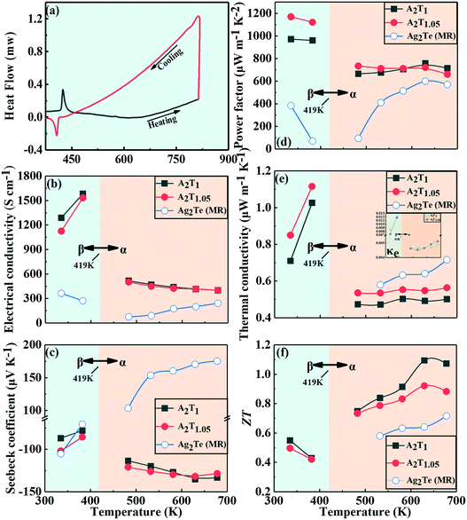 |
| | Fig. 8 Experimental and calculative thermoelectric properties of the Ag2Te bulk samples. (a) DSC curves during heating and cooling, (b) electrical conductivity, (c) Seebeck coefficient, (d) power factor, (e) thermal conductivity of κtotal and κel, and (f) ZT. The blue empty circle data were collected from the literature.38 | |
4. Thermoelectric properties of the A2Tx bulk
Fig. 8(b) shows the temperature dependence of the electrical conductivity of the A2T1 and A2T1.05 bulk samples. The electrical conductivities of the A2T1 and A2T1.05 samples increase gradually with increasing temperature below 419 K and then decrease with increasing temperature. The magnitude of the electrical conductivity also undergoes an abrupt change around the structural transition temperature. The literature data for electrical conductivity of Ag2Te prepared by solid state reaction and hot pressing are very similar to those of our samples. Fig. 8(c) shows the temperature dependence of the Seebeck coefficient of our A2T1 and A2T1.05 samples. The Seebeck coefficient is negative in the entire investigated temperature range, indicating that the majority of charge carriers are electrons and that the prepared samples are n-type semiconductors. The Seebeck coefficient and electrical conductivity are usually related, that is, higher electrical conductivities are often accompanied with lower absolute Seebeck coefficients; therefore, similar to the electrical conductivity, the Seebeck coefficient also undergoes changes in its behavior around the structural transition temperature. The literature data for the Seebeck coefficient of Ag2Te exhibit the similar temperature dependence but have a lower absolute value. The possible reason is that the hot pressing sample has a bigger grain size compared to our SPSed samples.
We now discuss the electrical transport properties of the components with different raw material ratios, which will help us to understand the effects of Ag on the transport properties of the components. For T < 419 K, where the monoclinic Ag2Te is stable, the transport properties of the A2T1 and A2T1.05 samples exhibit nonmetal-like temperature dependence. The results of EDS show that the A2Te1 sample has 1.63% excess Ag. The extra Ag doped into the Ag2Te increases the Te vacancies, increasing the electron concentration in the matrix. Therefore, the A2T1 sample has a higher carrier concentration than the A2T1.05 sample, which eventually leads to a higher electrical conductivity and lower absolute Seebeck coefficient at T < 419 K as shown in Fig. 8(b) and (c). When the temperature reaches 419 K, the transition from the monoclinic phase to the face centered cubic phase occurs. During this structural transition at approximately 419 K, all transport properties change dramatically. The electrical conductivities decrease rapidly at approximately 419 K and absolute Seebeck coefficients increase rapidly in this temperature range due to the low mobility and drastically decreased carrier concentration during the structural transition.36,37 It has been reported that the hole concentration of Ag2Te generally increases after the structural transition.36 This will lead to a reduction in the majority carrier concentrations. Consequently, as shown in Fig. 8(b) and (c), the electrical conductivities begin to decrease and the absolute Seebeck coefficients increase at approximately 450 K. Also affected by the Ag self-doping, the electrical conductivity of the A2T1 is higher than that of the A2T1.05, while the absolute Seebeck coefficient of A2T1 is lower than that of A2T1.05.
The calculated power factors are shown in Fig. 8(d), which show a decreasing trend with increasing temperature. The power factor was calculated as PF = S2σ, where S and σ stand for the Seebeck coefficient and electrical conductivity, the values of which were obtained experimentally. Similar to electrical conductivity, the power factor decreases significantly near the phase transition temperature. The power factor of the A2T1.05 sample reaches a maximum value of 1170 μW m−1 K−2 at 323 K. This value is much higher than those of the Ag2Te bulk samples prepared by Jung et al.38 using solid state reaction combined with hot pressing. We therefore believe that the use of silver telluride nanowires as precursor powder can greatly optimize the electrical properties of the silver telluride bulk materials. Meanwhile, it can be deduced from the larger power factor of the A2T1.05 sample that the Seebeck coefficient has a stronger impact on the power factor. When the temperature is below 528 K, the addition of silver increases the carrier mobility but has little effect on the carrier concentration, resulting in the decrease in the Seebeck coefficient that is clearly related to the increase of the electrical conductivity. But, as the temperature increases above 580 K, the Seebeck coefficient begins to decrease under the influence of the bipolar effect. The bipolar effect refers to the phenomenon that a large number of intrinsic excited carriers appear in thermoelectric materials with small band gaps as the temperature increases. These carriers contain electrons and holes that are excited at high temperature and move towards low temperature. The resulting Seebeck coefficient has the opposite sign and thus deteriorates the thermoelectric performance. The Ag in the A2T1 sample suppressed the intrinsic excitation of the holes, suppressing the influence of the bipolar effect and making the power factor of the A2T1 sample exceed that of the A2T1.05 sample. Generally, the addition of silver makes the power factor of Ag2Te slightly lower when the temperature is below 580 K, while, as the temperature increases, the addition of silver increases the power factor by suppressing the bipolar effect.
As usual, we will express the total thermal conductivity κtotal of solids as follows:
where
κlat is the lattice contribution and
κel is the electronic contribution.
κel can be calculated using the Wiedemann–Franz–Lorenz relation:
where
L is the Lorenz number,
σ is the electrical conductivity, and
T is the absolute temperature. Reduced Fermi energy was used to calculate the Lorenz number (
L) (
eqn (7)) which varies as the Seebeck value changes (
eqn (7)) with temperature or composition. The
L calculation was estimated in a traditional single parabolic band model (resulting in an
L with a deviation of less than 10% as compared with a more rigorous single non-parabolic band and multiple band model calculation), where the reduced Fermi energy was implicitly determined by the Seebeck values (
eqn (8)).
| |  | (7) |
| |  | (8) |
Variations of the κtotal and κel of Ag2Te with temperature are shown in Fig. 8(e). The κel is extremely low compared with the κtotal. This finding indicates that the thermal conductivity of the samples is mainly due to lattice thermal conductivity. As shown in Fig. 8(e), when the temperature is lower than 419 K, the thermal conductivity increases with increasing temperature and the values of thermal conductivity are close to 1. After the phase transition, the thermal conductivity of the samples decreased slightly with increasing temperature due to the increased thermal lattice vibrations. Meanwhile, the A2T1 sample showed a relatively lower thermal conductivity compared to the A2T1.05 sample due to the Ag self-doping. The Ag self-doping introduces Te vacancies that are highly effective phonon scatterers. The literature data for the thermal conductivity of Ag2Te is almost two times higher than that of our as-prepared Ag2Te samples. As shown in Fig. 7(a) and (b), the as-prepared Ag2Te samples prepared by solvothermal methods and spark plasma sintering have small grains and pores, which reduced the lattice thermal conductivity of our samples.
The ZT values of the n-type A2T1 and A2T1.05 are presented in Fig. 8. Before the phase transition temperature, the ZT value of the samples decreases with increasing temperature and reaches a maximum value of 0.5 at 323 K. Within the phase transition temperature range, the decrease in the thermal conductivity and the increase in the Seebeck coefficient lead to a significant increase in the ZT value. Then, the ZT value increases further with the increase in the temperature and then starts to decrease at 630 K. For the A2T1 sample, the ZT value reaches a maximum value of 1.1 at 630 K and then decreases with increasing temperature. For the A2T1.05 sample, the ZT value reaches a maximum value of 0.9 at 630 K, which is much higher than previously reported ZT values (0.4–0.6) for pure Ag2Te.38–41 In the measured temperature range, the higher ZT value of the A2T1 sample is mainly due to the Ag self-doping that leads to the increased carrier concentration and increased phonon scattering.
Conclusions
Pure phase Ag2Te nanowires were prepared by a simple solvothermal method without a template and surfactant. In the preparation process, the ratio of raw materials and the temperature of insulation play a crucial role in the composition and morphology of the nanowires. By adjusting the raw material ratio, we prepared silver-rich A2T1 and pure phase A2T1.05 samples. Based on the analysis of the composition and morphology of the nanowires obtained with different hydrothermal synthesis times and temperatures, we propose a possible mechanism for the formation of the nanowires. Conversely, nanowires are transformed into dense bulk materials by SPS. SPS changes the structure of the silver telluride nanowires, resulting in a significant improvement in electrical performance, so that the power factor of the A2T1.05 sample reaches 1170 μW m−1 K−2 at 323 K, but the thermal conductivity also increases. In this experiment, the phase transition temperature for silver telluride was approximately 419 K. The sample's performance changes after the phase transition. The high mobility of Ag atoms in the fcc structure significantly reduces the thermal conductivity, and the silver element enrichment in silver telluride further promotes the reduction of thermal conductivity. Therefore, the A2T1 sample finally shows the highest ZT value of 1.1 at 633 K. As an effective method for improving the thermoelectric properties of silver telluride, SPS of silver telluride nanowires should be further investigated.
Conflicts of interest
There are no conflicts to declare.
Acknowledgements
This work is supported by the National Natural Science Foundation of China (Grant No. 11764025).
References
- G. J. Snyder and E. S. Toberer, Nat. Mater., 2008, 7, 105–114 CrossRef CAS PubMed.
- M. S. Dresselhaus, G. Chen, M. Y. Tang, R. G. Yang, H. Lee, D. Z. Wang, Z. F. Ren, J. P. Fleurial and P. Gogna, Adv. Mater., 2007, 19, 1043–1053 CrossRef CAS.
- A. A. Shakouri, Annu. Rev. Mater. Res., 2011, 41, 399–431 CrossRef CAS.
- W. S. Liu, B. P. Zhang, J. F. Li and L. D. Zhao, J. Phys. D: Appl. Phys., 2007, 40, 6784 CrossRef CAS.
- J. Q. He, S. N. Girard, J. C. Zheng, L. D. Zhao, M. G. Kanatzidis and V. P. Dravid, Adv. Mater., 2012, 24, 4440–4444 CrossRef CAS PubMed.
- J. Q. He, I. D. Blum, H. Q. Wang, S. N. Girard, J. Doak, L. D. Zhao and D. N. Seidman, Nano Lett., 2012, 12, 5979–5984 CrossRef CAS PubMed.
- H. Wu, J. Carrete, Z. Zhang, Y. Qu, X. Shen, Z. Wang and J. Q. He, NPG Asia Mater., 2014, 6, e108 CrossRef CAS.
- G. Tang, W. Wei, J. Zhang, Y. Li, X. Wang, G. Xu and L. D. Zhao, J. Am. Chem. Soc., 2016, 138, 13647–13654 CrossRef CAS PubMed.
- H.-J. Choi, J. C. Johnson, R. He, S.-K. Lee, F. Kim, P. Pauzauskie, J. Goldberger, R. J. Saykally and P. Yang, J. Phys. Chem. B, 2003, 107, 8721 CrossRef CAS.
- J. Wang, Y. Zhao, J. Zhang, B. Yang, Y. Wang, D. Zhang, H. You and D. Ma, J. Phys. Chem. C, 2007, 111, 9177 CrossRef CAS.
- P. K. Mukherjee, D. Dutta, S. Bhattacharyya, A. Ghosh and D. Chakravoty, J. Phys. Chem. C, 2007, 111, 3914 CrossRef CAS.
- F. Xu and Y. Zhu, Adv. Mater., 2012, 24, 5117–5122 CrossRef CAS PubMed.
- Y. Z. Pei, N. A. Heinz and G. J. Snyder, J. Mater. Chem., 2011, 21, 18256–18260 RSC.
- J. Capps, F. Drymiotis, S. Lindsey and T. M. Tritt, Philos. Mag. Lett., 2010, 90, 677–681 CrossRef CAS.
- T. Day, F. Drymiotis, T. Zhang, D. Rhodes, X. Shi, L. Chen and G. J. Snyder, J. Mater. Chem. C, 2013, 1, 7568–7573 RSC.
- S. Ishiwata, Y. Shiomi, J. S. Lee, M. S. Bahramy, T. Suzuki, M. Uchida, R. Arita, Y. Taguchi and Y. Tokura, Nat. Mater., 2013, 12, 512–517 CrossRef CAS PubMed.
- M. Jafarov, F. Aliev, R. Hasanova and A. Saddinova, Semiconductors, 2012, 46, 861–865 CrossRef CAS.
- I. Karakaya and W. T. Thompson, J. Phase Equilib., 1991, 12, 56–63 CrossRef CAS.
- M. Fujikane, K. Kurosaki, H. Muta and S. Yamanaka, J. Alloys Compd., 2005, 393, 299–301 CrossRef CAS.
- F. F. Aliev, Semiconductors, 2003, 37, 1057–1060 CrossRef CAS.
- R. Z. Chen, D. S. Xu, G. L. Guo and L. L. Gui, J. Mater. Chem., 2002, 12, 2435 RSC.
- A. M. Qin, Y. P. Fang, P. F. Tao, J. Y. Zhang and C. Y. Su, Inorg. Chem., 2007, 46, 7403 CrossRef CAS PubMed.
- P. F. Zuo, S. Y. Zhang, B. K. Jin, Y. P. Tian and J. X. Yang, J. Phys. Chem. C, 2008, 112, 14825 CrossRef CAS.
- F. Drymiotis, T. W. Day, D. R. Brown, N. A. Heinz and G. Jeffrey Snyder, Appl. Phys. Lett., 2013, 103, 143906 CrossRef.
- F. Li, C. Hu, Y. Xiong, B. Wan, W. Yan and M. Zhang, J. Phys. Chem. C, 2008, 112, 16130–16133 CrossRef CAS.
- D. Cadavid, M. Ibanez, A. Shavel, O. J. Dura, M. A. Lopez de la Torre and A. Cabot, J. Mater. Chem. A, 2013, 1, 4864–4870 RSC.
- W. Zhou, W. Zhao, Z. Lu, J. Zhu, S. Fan, J. Ma, H. H. Hng and Q. Yan, Nanoscale, 2012, 4, 3926–3931 RSC.
- G.-H. Dong and Y.-J. Zhu, CrystEngComm, 2012, 14, 1805–1811 RSC.
- M. G. Kanatzidis, Chem. Mater., 2010, 22, 648–659 CrossRef CAS.
- C. J. Vineis, A. Shakouri, A. Majumader and M. G. Kanatzidis, Adv. Mater., 2010, 22, 3970–3980 CrossRef CAS PubMed.
- W. Liu, X. Yan, G. Chen and Z. Ren, Nano Energy, 2012, l, 42–56 CrossRef.
- J. Xu, H. Li, B. Du, X. Tang, Q. Zhang and C. Uher, J. Mater. Chem., 2010, 20, 6138 RSC.
- F. H. Lin and C. J. Liu, Green Chem., 2016, 18, 5288–5294 RSC.
- F. Xiao, G. Chen, Q. Wang, L. Wang, J. Pei and N. Zhou, J. Solid State Chem., 2010, 183, 2382–2388 CrossRef CAS.
- O. G. Schmidt and K. Eberl, Nature, 2001, 410, 168 CrossRef CAS PubMed.
- L. Zhang, Z. Ai, F. Jia, L. Liu, X. Hu and J. C. Yu, Chem. – Eur. J., 2006, 12, 4185–4190 CrossRef CAS PubMed.
- S. A. Aliev, Z. F. Agaev and E. I. Zul'figarov, Semiconductors, 2007, 41, 1027–1032 CrossRef CAS.
- D.-Y. Jung, K. Kurosaki, Y. Ohishi, H. Muta and S. Yamanaka, Mater. Trans., 2012, 7, 1216–1219 CrossRef.
- I. S. Chuprakov and K. H. Dahmen, Appl. Phys. Lett., 1998, 72, 2165–2167 CrossRef CAS.
- W. W. Zhou, W. Y. Zhao, Z. Y. Lu, J. X. Zhu, S. F. Fan, J. Ma, H. H. Hng and Q. Y. Yan, Nanoscale, 2012, 4, 3926–3931 RSC.
- J. Capps, F. Drymiotis, S. Lindsey and T. M. Tritt, Philos. Mag. Lett., 2010, 90, 677–681 CrossRef CAS.
|
| This journal is © The Royal Society of Chemistry 2019 |
Click here to see how this site uses Cookies. View our privacy policy here. 
 *
*