
 Open Access Article
 This Open Access Article is licensed under a Creative Commons Attribution-Non Commercial 3.0 Unported Licence
Photoemission spectroscopy study of structural defects in molybdenum disulfide (MoS2) grown by chemical vapor deposition (CVD)†
Ali
Syari’ati
 ,
Sumit
Kumar
,
Amara
Zahid
,
Abdurrahman
Ali El Yumin
,
Jianting
Ye
and
Petra
Rudolf
*
,
Sumit
Kumar
,
Amara
Zahid
,
Abdurrahman
Ali El Yumin
,
Jianting
Ye
and
Petra
Rudolf
*
Zernike Institute for Advanced Materials, University of Groningen, Nijenborgh 4, 9747 AG Groningen, The Netherlands. E-mail: p.rudolf@rug.nl
First published on 3rd August 2019
Abstract
The fingerprint of structural defects in CVD grown MoS2 was revealed by means of X-ray Photoelectron Spectroscopy (XPS). These defects can be partially healed by grafting thiol-functionalized molecules. The functionalization does not alter the semiconducting properties of MoS2 as confirmed by the photoluminescence spectra.
The extraordinary properties of graphene have sparked increasing interest in other layered materials like Transition Metal Dichalcogenides (TMDCs). TMDCs consist of layers held together by van der Waals (vdW) interaction like graphene layers but here one layer comprises a transition metal atom sheet sandwiched between two chalcogen atom sheets via covalent bonds. The weak vdW interaction between the layers can be exploited to isolate two-dimensional (2D) flakes by mechanical,1,2 chemical3 and liquid exfoliation,4–6 but these ultrathin crystals can also be synthesized on suitable substrates by Chemical Vapor Deposition (CVD)7–10 or Molecular Beam Epitaxy (MBE).11 MoS2 has received special attention among TMDCs because its electronic and optoelectronic properties promise well for application in transistors,2,12,13 sensors,14 and as a catalyst.15,16 CVD is the only upscalable method that allows obtaining large domains of single crystalline MoS2 with sizes reaching hundreds of μm and an electron mobility which approaches that of exfoliated MoS2.17 However, so far defects seem unavoidable in CVD grown and exfoliated MoS2,18 and can be exploited as catalytic sites for e.g. hydrogen evolution reactions.19 On the other hand, these defects decrease the mobility and photoluminescence (PL) intensity of MoS220–22 and strategies to heal them need to be developed. Zhou et al. reported the direct observation by scanning tunneling microscopy of intrinsic structural defects in CVD grown MoS2,23 namely sulfur and molybdenum vacancies. Sulfur vacancies can be filled by adsorption of thiol molecules24 and this strategy can also serve to tune the properties of MoS2 crystals by functional groups attached to the thiol moiety.25–27
In this communication, we monitor structural defects in CVD grown MoS2 by means of X-ray Photoelectron Spectroscopy (XPS). We demonstrate that the defect density can be increased by thermal annealing, introducing also another type of structural defect. We prove that thiol-terminated cysteine molecules can partially heal the defects by covalently binding to MoS2 as depicted in Scheme 1. This result differs from the findings of Chen et al., who reported that cysteine molecules merely physisorb on the surface.28
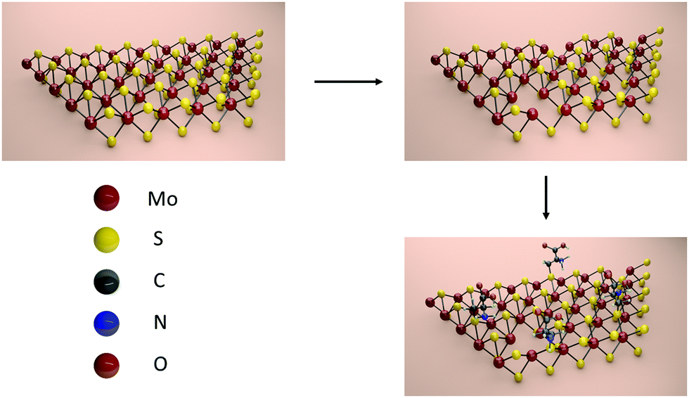 | ||
| Scheme 1 Functionalization of MoS2 with cysteine molecules via first creating defects through thermal annealing and then filling them with thiol-terminated cysteine. | ||
MoS2 crystalline flakes were grown by CVD on oxide-passivated Si wafers (Prime Wafers) as explained in the ESI,† where we detail our reproducible approach to obtain large domain single layer MoS2.29 Optical microscopy images showed MoS2 crystal sizes varying from several to hundreds of μm (see the ESI†). Atomic Force Microscopy and Raman spectroscopy confirmed that MoS2 (see the ESI†) consists of a single layer. XPS spectra (for experimental details see the ESI†) of the freshly grown sample were collected to minimize contamination from air; 2–4 spots were analysed on each sample to confirm homogeneity. The XPS signal due to adventitious carbon located at 284.8 eV was used as a binding energy (BE) reference.
The spectral region shown in Fig. 1(a) contains both the Mo3d and the S2s core level signals and can be fitted with three Mo3d doublets and two singlet peaks (S2s). The most intense doublet peak, located at a BE of 229.6 eV, is attributed to Mo4+ (i-Mo4+), the charge state of molybdenum in MoS2. The doublet peak located at 1.7 eV higher BE stems from defect Mo4+ (d-Mo4+), i.e. corresponding to Mo atoms close to sulfur vacancies (VS).30,31 Finally, the doublet peak at 233.0 eV BE is due to Mo6+ of the unreacted precursor MoO3,32 which is always found as a contaminant on CVD grown MoS2. The most intense singlet peak is due to the S2s emission from defect-free regions of MoS2, while the additional singlet peak at 227.6 eV corresponds to sulfur close to a defect. The sulfur chemical environment can be more clearly studied by means of the S2p core level spectrum, shown in Fig. 1(d), where two doublets, peaked at 162.4 eV and 163.1 eV, respectively, are observed. We attribute the most intense contribution to intrinsic S (i-S) and the higher BE doublet to sulfur near S vacancies (d-S). This observation is very important because it constitutes the spectroscopic proof of the presence of unsaturated Mo atoms in CVD-grown MoS2, already observed microscopically by Zhou et al.23
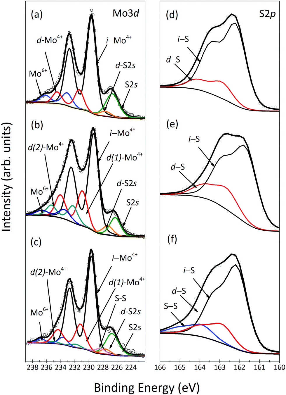 | ||
| Fig. 1 XPS spectra: Mo3d and S2p core level regions of MoS2 as-grown (a and d), annealed before (b and e) and after functionalization (c and f). | ||
Thermal annealing is known to induce desorption of S atoms from the MoS2 nanosheet.33Fig. 1(b) shows the XPS spectrum of the Mo3d core level region of the annealed sample, which, apart from a small chemical shift due to band bending,33 clearly presents a different line shape than the as-grown sample and requires an additional Mo component in the fit. We attribute this new doublet peaked at 231.6 eV (d(2)-Mo4+) to unsaturated Mo atoms close to a more complex defect present in the MoS2 crystal. We observe a decrease in Mo and S spectral intensity as well as in the S and Mo intensity ratio after annealing. The calculation of the formation energy of the various defects in MoS2,31 namely of a molybdenum vacancy (VMo) and divacancies implying either a missing MoS moiety (VMoS) or two missing sulfur atoms (VSS), gives the lowest value for VMo, and only a 0.2 eV higher value for VMoS and VSS, making it difficult to discriminate which defects are formed after annealing. Since d(2)-Mo4+ appears at a higher BE than d(1)-Mo4+ and i-Mo4+ we can conclude that it is associated with the loss of S atoms; in fact more than one missing S implies even more positive charge on the surrounding Mo atoms.31 After annealing, we also observe a 10 ± 2% intensity increase of the component attributed to d(1)-Mo4+, confirming the assignment to VS in the MoS2 nanosheet; moreover the d(1)-Mo4+ component is shifted to lower BE, confirming additional loss of S in the surroundings of Vs.34
The desorption of S atoms is also observed in the S2p spectrum of the annealed sample, depicted in Fig. 1(e), where the intensity of the component assigned to the d-S peak increased by 11%. The rigid binding energy shift was also observed for S2p spectral lines upon annealing, similar to the result reported by Donarelli et al.33
To explore whether these structural defects can be healed by thiol-functionalized molecules, we exposed MoS2 to thiol-terminated cysteine. Functionalization of freshly grown MoS2 resulted in a barely noticeable change in the XPS spectra due to undesired contamination blocking adsorption sites (see the ESI†). The XPS spectra of the Mo3d and the S2s core level region and the S2p core level region of functionalized annealed MoS2 are shown in Fig. 1(c) and (f), respectively. In the spectrum of Fig. 1(c), one notes that the exposure to thiol-functionalized cysteine induced a 3 ± 2% decrease in the d(1)-Mo4+ spectral intensity and a 8 ± 2% decrease in the d(2)-Mo4+ spectral intensity. Chu et al. reported that monosulfur vacancies can act as the centers for the functionalization because when one thiol molecule is attached it facilitates the adsorption of other molecules to neighbouring vacancies in the range of 9–36 Å2 from the first adsorbate.35 Interestingly, the two components are also shifted towards higher BE, with the d(2)-Mo4+ doublet now peaked at 232.0 eV and the d(1)-Mo4+ doublet peaked at 231.2 eV. This observation indicates that the adsorbed molecules not only heal the structural defects but also promote charge transfer, a mechanism, which could be used to tailor the electronic properties of MoS2. In agreement with a previous discussion of the Mo spectra, upon functionalization (Fig. 1(f)) a noticeable decrease of 10.8% of the intensity of the d-S component was observed, confirming preferential healing of monosulfur vacancies. Furthermore, a new contribution appeared at 164.2 eV, attributed to S–S bonds,28 corroborating adsorption of a second cysteine molecule close to a first one, which also supports the result of the Mo3d spectra.36
Confirmation for the presence of cysteine grafted onto the MoS2 basal plane also comes from the XPS spectra of the C1s and N1s core level regions of the functionalized MoS2 shown in Fig. 2. In Fig. 2(a), the adventitious carbon with C–C and C–O bonds was observed in the as-grown sample. Upon functionalization, as expected, the spectral intensity of these components increased, together with the appearance of a new component at 286.0 eV due to C–S bonds; the relative increases in intensity agree with what is expected from the molecular structure of cysteine. In Fig. 2(b), the nitrogen peak observed at 403.4 eV corresponds to the N–C bond, again as expected for adsorbed cysteine.
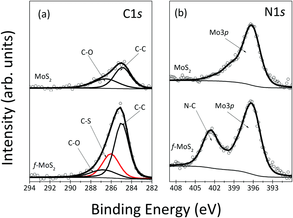 | ||
| Fig. 2 XPS spectra of C1s (a) and N1s (b) core level regions of as-grown MoS2 and after functionalization of annealed MoS2. | ||
FTIR spectroscopy is a fast and non-destructive tool to confirm the covalent functionalization of the MoS2 nanosheet;28,37,38 therefore, we collected the Attenuated Total Reflection Fourier Transform Infra-Red (ATR-FTIR) spectrum of functionalized MoS2 to support the XPS data. The spectrum is shown in Fig. 3 together with the spectrum of cysteine for reference. The S–H stretching vibration (νS–H) at 2549 cm−1, clearly observed in cysteine but absent for functionalized MoS2, points to H splitting off when the molecules bind to the MoS2 basal plane.39 Furthermore, the presence of a band at 700 cm−1, typical of the C–S stretching vibration, can be taken as evidence of the successful functionalization.40 The presence of this feature in both samples proves the presence of cysteine on MoS2 and supports the XPS data.
Unlike another covalent functionalization strategy,41,42 which requires transformation of the semiconducting 2H-MoS2 phase into metallic MoS2 (1T-MoS2), the covalent functionalization performed in this work preserves the semiconducting nature of the TMDC, as demonstrated by the photoluminescence (PL) spectrum in Fig. 4. Upon functionalization, MoS2 shows a PL peak at 668 nm, which is absent in the case of 1T-MoS2.24 However, the PL intensity decreased and the peak is slightly blue-shifted due to the doping from the cysteine molecules, in agreement with the XPS results.
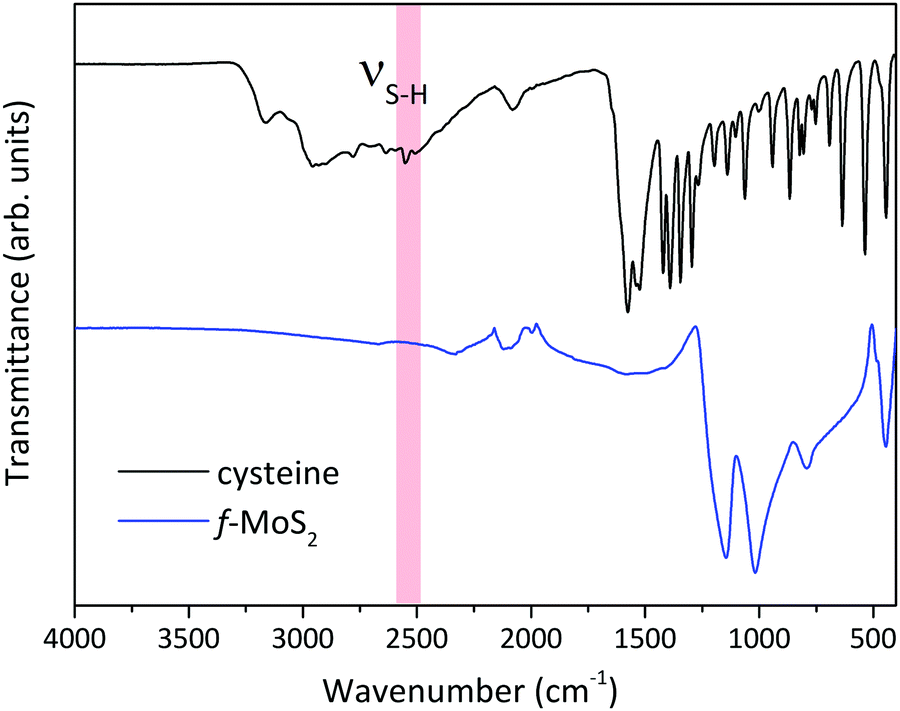 | ||
| Fig. 3 ATR-FTIR spectra of cysteine and defect-rich MoS2 after functionalization with thiol-terminated cysteine. | ||
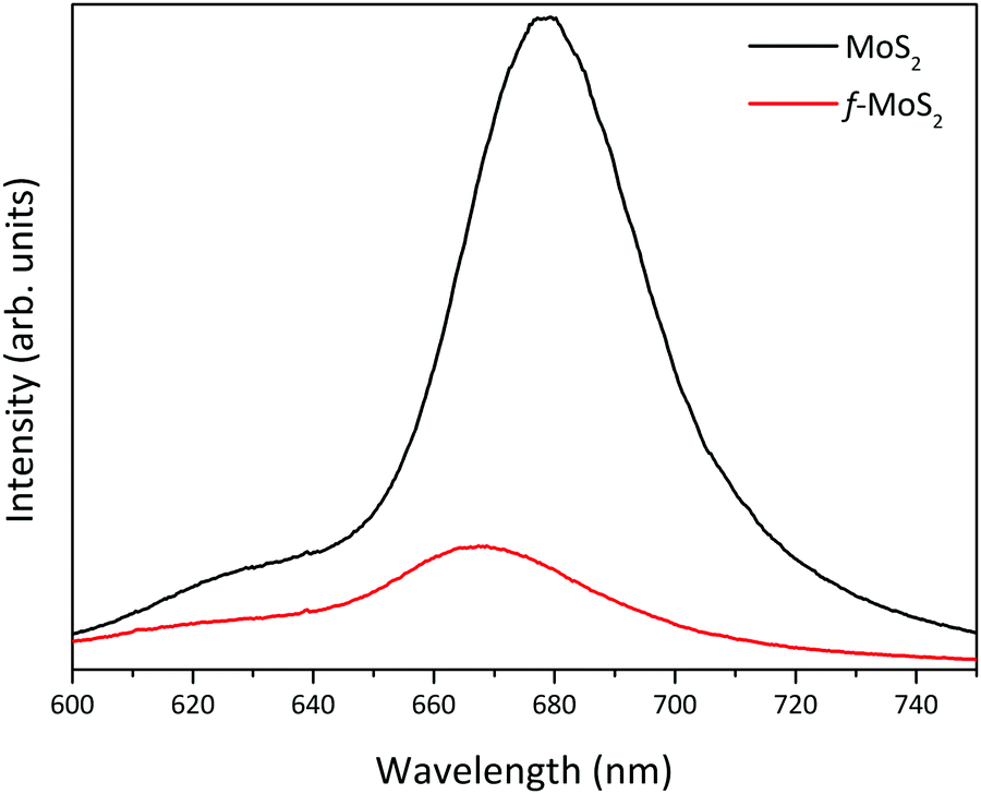 | ||
| Fig. 4 PL spectra before (MoS2) and after functionalization (f-MoS2). | ||
In conclusion, we identified the XPS fingerprint of the structural defects in CVD grown MoS2 and demonstrated that when thermal annealing causes sulfur to desorb from the basal plane of MoS2, vacancies with more than one missing sulfur atom are created. Most importantly we proved that partial filling of vacancies is possible via covalent functionalization of defective MoS2 with thiol-terminated cysteine. After functionalization MoS2 maintains its semiconducting characteristics.
A. Syari’ati thanks the Indonesian Endowment Fund for Education (LPDP) for supporting his PhD study. This work was supported by the Advanced Materials Research Program of the Zernike National Research Centre under the Bonus Incentive Scheme of the Dutch Ministry for Education, Culture and Science.
Conflicts of interest
There are no conflicts to declare.Notes and references
- Q. H. Wang, K. Kalantar-Zadeh, A. Kis, J. N. Coleman and M. S. Strano, Nat. Nanotechnol., 2012, 7, 699–712 CrossRef CAS PubMed.
- Y. Zhang, J. Ye, Y. Matsuhashi and Y. Iwasa, Nano Lett., 2012, 12, 1136–1140 CrossRef CAS PubMed.
- G. Eda, H. Yamaguchi, D. Voiry, T. Fujita, M. Chen and M. Chhowalla, Nano Lett., 2011, 11, 5111–5116 CrossRef CAS PubMed.
- J. N. Coleman, M. Lotya, A. O’Neill, S. D. Bergin, P. J. King, U. Khan, K. Young, A. Gaucher, S. De, R. J. Smith, I. V. Shvets, S. K. Arora, G. Stanton, H.-Y. Kim, K. Lee, G. T. Kim, G. S. Duesberg, T. Hallam, J. J. Boland, J. J. Wang, J. F. Donegan, J. C. Grunlan, G. Moriarty, A. Shmeliov, R. J. Nicholls, J. M. Perkins, E. M. Grieveson, K. Theuwissen, D. W. McComb, P. D. Nellist and V. Nicolosi, Science, 2011, 331, 568–571 CrossRef CAS PubMed.
- G. Cunningham, M. Lotya, C. S. Cucinotta, S. Sanvito, S. D. Bergin, R. Menzel, M. S. P. Shaffer and J. N. Coleman, ACS Nano, 2012, 6, 3468–3480 CrossRef CAS PubMed.
- H. B. Sim, J. Y. Lee, B. Park, S. J. Kim, S. Kang, W. H. Ryu and S. C. Jun, Nano Res., 2016, 9, 1709–1722 CrossRef CAS.
- J. Jeon, S. K. Jang, S. M. Jeon, G. Yoo, Y. H. Jang, J.-H. Park and S. Lee, Nanoscale, 2014, 1–10 Search PubMed.
- Y. Lee, S. Park, H. Kim, G. H. Han, Y. H. Lee and J. Kim, Nanoscale, 2015, 7, 11909–11914 RSC.
- L. Tao, K. Chen, Z. Chen, W. Chen, X. Gui, H. Chen, X. Li and J.-B. Xu, ACS Appl. Mater. Interfaces, 2017, 9, 12073–12081 CrossRef CAS PubMed.
- Y. Kim, H. Bark, G. H. Ryu, Z. Lee and C. Lee, J. Phys.: Condens. Matter, 2016, 28, 6 Search PubMed.
- D. Fu, X. Zhao, Y.-Y. Zhang, L. Li, H. Xu, A.-R. Jang, S. I. Yoon, P. Song, S. M. Poh, T. Ren, Z. Ding, W. Fu, T. J. Shin, H. S. Shin, S. T. Pantelides, W. Zhou and K. P. Loh, J. Am. Chem. Soc., 2017, 139, 9392–9400 CrossRef CAS PubMed.
- B. Radisavljevic, A. Radenovic, J. Brivio, V. Giacometti and A. Kis, Nat. Nanotechnol., 2011, 6, 147–150 CrossRef CAS PubMed.
- J. Kang, W. Liu and K. Banerjee, Appl. Phys. Lett., 2014, 104, 093106 CrossRef.
- A. Smolyanitsky, B. I. Yakobson, T. A. Wassenaar, E. Paulechka and K. Kroenlein, ACS Nano, 2016, 10, 9009–9016 CrossRef CAS PubMed.
- M. A. Lukowski, A. S. Daniel, F. Meng, A. Forticaux, L. Li and S. Jin, J. Am. Chem. Soc., 2013, 135, 10274–10277 CrossRef CAS PubMed.
- E. E. Benson, H. Zhang, S. A. Schuman, S. U. Nanayakkara, N. D. Bronstein, S. Ferrere, J. L. Blackburn and E. M. Miller, J. Am. Chem. Soc., 2018, 140, 441–450 CrossRef CAS PubMed.
- J. Chen, W. Tang, B. Tian, B. Liu, X. Zhao, Y. Liu, T. Ren, W. Liu, D. Geng, H. Y. Jeong, H. S. Shin, W. Zhou and K. P. Loh, Adv. Sci., 2016, 3, 1500033 CrossRef PubMed.
- J. Hong, Z. Hu, M. Probert, K. Li, D. Lv, X. Yang, L. Gu, N. Mao, Q. Feng, L. Xie, J. Zhang, D. Wu, Z. Zhang, C. Jin, W. Ji, X. Zhang, J. Yuan and Z. Zhang, Nat. Commun., 2015, 6, 6293 CrossRef CAS PubMed.
- G. Ye, Y. Gong, J. Lin, B. Li, Y. He, S. T. Pantelides, W. Zhou, R. Vajtai and P. M. Ajayan, Nano Lett., 2016, 16, 1097–1103 CrossRef CAS PubMed.
- H. Nan, Z. Wang, W. Wang, Z. Liang, Y. Lu, Q. Chen, D. He, P. Tan, F. Miao, X. Wang, J. Wang and Z. Ni, ACS Nano, 2014, 8, 5738–5745 CrossRef CAS PubMed.
- W. Su, L. Jin, X. Qu, D. Huo and L. Yang, Phys. Chem. Chem. Phys., 2016, 18, 14001–14006 RSC.
- Z. Yu, Y. Pan, Y. Shen, Z. Wang, Z.-Y. Ong, T. Xu, R. Xin, L. Pan, B. Wang, L. Sun, J. Wang, G. Zhang, Y. W. Zhang, Y. Shi and X. Wang, Nat. Commun., 2014, 5, 5290 CrossRef CAS PubMed.
- W. Zhou, X. Zou, S. Najmaei, Z. Liu, Y. Shi, J. Kong, J. Lou, P. M. Ajayan, B. I. Yakobson and J. C. Idrobo, Nano Lett., 2013, 13, 2615–2622 CrossRef CAS PubMed.
- D. M. Sim, M. Kim, S. Yim, M. J. Choi, J. Choi, S. Yoo and Y. S. Jung, ACS Nano, 2015, 9, 12115–12123 CrossRef CAS PubMed.
- R. Canton-Vitoria, Y. Sayed-Ahmad-Baraza, M. Pelaez-Fernandez, R. Arenal, C. Bittencourt, C. P. Ewels and N. Tagmatarchis, npj 2D Mater. Appl., 2017, 1, 13 CrossRef.
- P. Vishnoi, A. Sampath, U. V. Waghmare and C. N. R. Rao, Chem. – A Eur. J., 2017, 23, 886–895 CrossRef CAS PubMed.
- E. P. Nguyen, B. J. Carey, J. Z. Ou, J. Van Embden, E. Della Gaspera, A. F. Chrimes, M. J. S. Spencer, S. Zhuiykov, K. Kalantar-Zadeh and T. Daeneke, Adv. Mater., 2015, 27, 6225–6229 CrossRef CAS PubMed.
- X. Chen, N. C. Berner, C. Backes, G. S. Duesberg and A. R. McDonald, Angew. Chem., Int. Ed., 2016, 55, 5803–5808 CrossRef CAS PubMed.
- A. Syari’ati, A. Ali, E. Yumin, T. Zehra, B. Kooi, J. Ye and P. Rudolf, unpublished.
- I. S. Kim, V. K. Sangwan, D. Jariwala, J. D. Wood, S. Park, K. S. Chen, F. Shi, F. Ruiz-Zepeda, A. Ponce, M. Jose-Yacaman, V. P. Dravid, T. J. Marks, M. C. Hersam and L. J. Lauhon, ACS Nano, 2014, 8, 10551–10558 CrossRef CAS PubMed.
- S. Haldar, H. Vovusha, M. K. Yadav, O. Eriksson and B. Sanyal, Phys. Rev. B: Condens. Matter Mater. Phys., 2015, 92, 1–12 CrossRef.
- D. Ganta, S. Sinha and R. T. Haasch, Surf. Sci. Spectra, 2014, 21, 19–27 CrossRef CAS.
- M. Donarelli, F. Bisti, F. Perrozzi and L. Ottaviano, Chem. Phys. Lett., 2013, 588, 198–202 CrossRef CAS.
- M. A. Baker, R. Gilmore, C. Lenardi and W. Gissler, Appl. Surf. Sci., 1999, 150, 255–262 CrossRef CAS.
- X. S. Chu, A. Yousaf, D. O. Li, A. A. Tang, A. Debnath, D. Ma, A. A. Green, E. J. G. Santos and Q. H. Wang, Chem. Mater., 2018, 30, 2112–2128 CrossRef CAS.
- K. C. Knirsch, N. C. Berner, H. C. Nerl, C. S. Cucinotta, Z. Gholamvand, N. McEvoy, Z. Wang, I. Abramovic, P. Vecera, M. Halik, S. Sanvito, G. S. Duesberg, V. Nicolosi, F. Hauke, A. Hirsch, J. N. Coleman and C. Backes, ACS Nano, 2015, 9, 6018–6030 CrossRef CAS PubMed.
- C. Backes, N. C. Berner, X. Chen, P. Lafargue, P. LaPlace, M. Freeley, G. S. Duesberg, J. N. Coleman and A. R. McDonald, Angew. Chem., Int. Ed., 2015, 54, 2638–2642 CrossRef CAS PubMed.
- X. Chen and A. R. McDonald, Adv. Mater., 2016, 5738–5746 CrossRef CAS PubMed.
- E. Satheeshkumar, A. Bandyopadhyay, M. B. Sreedhara, S. K. Pati, C. N. R. Rao and M. Yoshimura, ChemNanoMat, 2017, 3, 172–177 CrossRef CAS.
- S. F. Parker, Chem. Phys., 2013, 424, 75–79 CrossRef CAS.
- S. Presolski and M. Pumera, Mater. Today, 2016, 19, 140–145 CrossRef CAS.
- D. Voiry, A. Goswami, R. Kappera, C. D. C. C. E. Silva, D. Kaplan, T. Fujita, M. Chen, T. Asefa and M. Chhowalla, Nat. Chem., 2015, 7(1), 45–49 CrossRef CAS PubMed.
Footnote |
| † Electronic supplementary information (ESI) available. See DOI: 10.1039/c9cc01577a |
| This journal is © The Royal Society of Chemistry 2019 |