
Advancements in fractal plasmonics: structures, optical properties, and applications
Gregory Q.
Wallace
and
François
Lagugné-Labarthet
 *
*
Department of Chemistry and the Centre for Advanced Materials and Biomaterials Research, University of Western Ontario, 1151 Richmond Street, London, Ontario N6A 5B7, Canada. E-mail: flagugne@uwo.ca
First published on 31st October 2018
Abstract
The structural characteristics of plasmonic nanostructures directly influence their plasmonic properties, and therefore, their potential role in applications ranging from sensing and catalysis to light- and energy-harvesting. For a structure to be compatible with a selected application, it is critical to accurately tune the plasmonic properties over a specific spectral range. Fabricating structures that meet these stringent requirements remains a significant challenge as plasmon resonances are generally narrow with respect to the considered selected spectral range. Adapted from their well-established role in GHz applications, plasmonic fractal structures have emerged as architectures of interest due to their ability to support multiple tunable resonances over broad spectral domains. Here, we review the advancements that have been made in the growing field of fractal plasmonics. Iterative and space-filling geometries that can be prepared by advanced nanofabrication techniques, notably electron-beam lithography, are presented along with the optical properties of such structures and metasurfaces. The distributions of electromagnetic enhancement for some of these fractals is shown, along with how the resonances can be mapped experimentally. This review also explores how fractal structures can be used for applications in solar cell and plasmon-based sensing applications. Finally, the future areas of physical and analytical science that could benefit from fractal plasmonics are discussed.
1. Introduction
Conductive structures with sub-wavelength dimensions support localized surface plasmon resonances (LSPRs), the properties of which are dependent on the geometric parameters of the structure and the opto-geometric specifications of the experiment. Depending on the material and geometry of the nanostructure, the LSPRs can span from the ultraviolet to the far-infrared (-IR). Upon illumination, nanoscale regions of electromagnetic (EM) enhancement, referred to as hot-spots, are generated at the surface of the structure. Because of these broad optical properties, plasmonic nanostructures have found use in a variety of applications including: catalysis,1,2 medicine,3,4 surface chemistry,5–7 photovoltaics,8 and most notably sensing.9–12 Typically, gold and silver are used as the plasmonic material as they exhibit strong LSPRs in the visible region. An emerging area of interest focusses on exploring the plasmonic properties of alternative metals and conductive materials to have compatibility with different spectral domains and applications.13–26Although the choice of metal influences the plasmonic properties, the geometry of the structure plays a critical role in tuning the resonance positions and EM enhancement. Given a fixed shape, the size of the structure directly influences the spectral position(s) of the LSPR(s). This relationship is often found to be linear, providing a straightforward means of tuning the resonance to specific wavelengths or spectral domains of interest. The shape of the structure influences both the spectral position of the LSPR(s) and the resulting local EM enhancement. In the case of anisotropic nanostructures, such as nanorods and nanoprisms, the confinement of the EM field depends strongly on the polarization orientation of the impinging light with respect to the structure. For example, the enhancement along the length of a nanorod typically occurs in the near- to mid-IR, whereas the LSPR long the orthogonal direction (the width of the nanorod) can be found in the visible region.27 Precise control over these opto-geometric properties is crucial in maximizing the tunability of the structure and the enhancement capabilities.
Given advancements in synthetic protocols and nanofabrication techniques, one simply needs to perform a quick search of the literature to face an incredibly vast range of structures that have been fabricated. However, regardless of the structure, plasmon resonances often occur only within a narrow spectral domain. Broadening the resonance(s) or introducing a series of resonances can yield not only multispectral compatibility, but also compatibility with multiple applications. In three-dimensional designs, introducing alternating material layers within the structure has been used to broaden the resonance and introduce multiple resonances.28–30 The more common approach however is to design pseudo-planar structures with highly tailored geometries,31–35 including those with fractal-like properties.
The term “fractal”, coined by Benoit Mandelbrot,36 describes curves that have repeating patterns that are often obtained by applying some iterative transformation on a system. Applied to plasmonic structures, this self-similarity, whether exact, quasi, or statistical, leads to a broadband multimodal EM response. For example, macroscopic fractal antennas are used for applications in the GHz range.37–40 By rationally engineering the fractal dimensions, the broadband response can be tuned to specific spectral domains. Fabricating the fractals with plasmonic materials and nanoscale dimensions leads to the broadband response to be a series of discrete plasmonic responses, namely LSPRs. Consequently, the term fractal plasmonics has since been used to describe this phenomenon.
This review serves as an introduction to the field of fractal plasmonics. Although the use of fractal-like plasmonic aggregates as a means of enhancing Raman signals dates to the 1980s,41 it is really only in the last decade that the area of fractal plasmonics has revealed its potential due to the development of accurate fabrication methods such as electron-beam lithography (EBL). We therefore emphasize the advancements that have been made in this expanding field. We begin by highlighting the fractal geometries that have been studied, along with their corresponding plasmonic properties. We then provide an overview on how these properties can be modelled and experimentally measured, and how the multiresonant nature of the structure can be explained using the hybridization model. Due to the broad plasmonic properties, several applications involving fractal nanostructures have emerged, and are discussed. We then describe specific areas of future expansion that can be explored.
2. Optical properties of different fractal geometries
As the definition for what defines as a fractal is quite broad, many nanostructures have been described as exhibiting a fractal-like appearance. In this section, we focus on geometries that have recognizable or well-defined structural properties that classify them as fractals. Depending on the nature of the fractal, different methods ranging from synthetic to lithographic processes can be used to prepare the fractals. In most cases, the described fractals were prepared by lithographic techniques, notably EBL and focused ion beam milling. This section intends to provide an overview of general classifications of fractals and their optical properties and is therefore not to be considered an exhaustive list of all possible fractal geometries.2.1 Dendritic-like fractals
Early work involving the electrodeposition of copper demonstrated that the resulting microstructures exhibit what have since been described as a dendrimer-like or dendritic appearance (Fig. 1A).42 In the intervening years, other electrochemical,43–46 and synthetic processes have been used to prepare plasmonic dendrimers.47–50 Furthermore, these approaches have been used to fabricate dendrimers with a variety of metal and material compositions including: silver,44,46 gold,47,50 platinum,48 copper/silver,43 graphene oxide coated silver,45 and palladium on graphene nanoplatelets.49 SEM (Fig. 1B) and TEM (Fig. 1C) images reveal that many of the structures exhibit a palm leaf-like appearance. With this geometry, the fractals exhibit important optical properties. As shown in Fig. 1D, the plasmon resonance of the structure spans from 500 to above 1000 nm.50 The broadness of this resonance can be attributed to several parameters. As the electron microscopy images clearly show, the fractals are composed of branches with different lengths, widths, and geometries. In addition, the adjacent branches have varying gap sizes. Much like aggregates of nanoparticles,51 each nanoscale difference leads to a slightly different resonance position, culminating in an overall broad resonance. Beyond exhibiting a broad resonance, the highly branched nature of the fractal provides a dense distribution of EM enhancement over the surface of the fractal.52 In the case of the highlighted studies, these structures are typically used to enhance Raman signals,43–47,50 and drive chemical reactions at surfaces.46,48,49 Surface-enhanced fluorescence has also benefitted from the use of fractal silver structures prepared electrically driven processes.53,54 A significant restriction of these approaches is the limited control over the final shape, size, and geometry of the fractal. Overcoming these limitations can be achieved by using top-down lithographic procedures.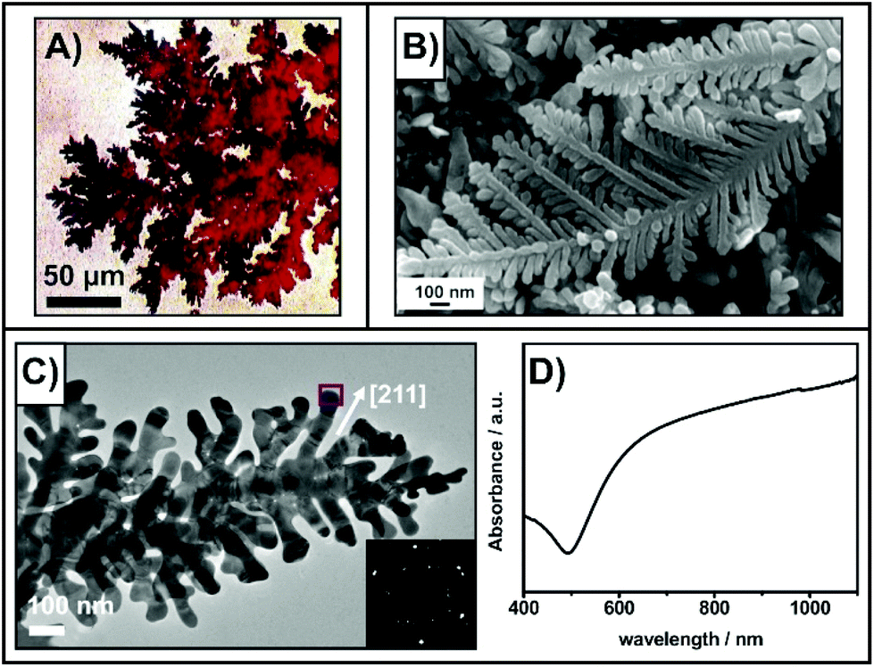 | ||
| Fig. 1 (A) Optical image of dendritic microstructures prepared by pulsed-current deposition of copper.42 (B) SEM image of silver dendrites on a copper substrate prepared by galvanic replacement.45 (C) TEM image gold nanodendrites prepared using a poly(ionic liquid) method.50 (D) absorbance spectrum of the gold nanodendrites. Reprinted and adapted from ref. 42, 50, and 45. Copyrights Elsevier 1998 and 2017, and The Royal Society of Chemistry respectively. | ||
In this regard, EBL is well suited to the fabrication of fractal structures as the technique has a resolution that is better than 10 nm.55,56 To date, EBL prepared dendrimers have been shown to exhibit distinct and intense absorbances in the near- to mid-IR.57–60 Based on the Cayley Tree geometry (Fig. 2A),58 the design of the fractal is as follows. In the first-order generation, there are n number of branches, while in the second-order and above generations, there are number of branches is n − 1. As a result, it is possible to design a wide range of possible geometries simply by changing the order of the fractal and the number of inner branches. Only by top-down approaches is it possible to readily examine how these parameters, along with classical changes such as altering the length of the nanorods in the fractal, effects the plasmonic properties.
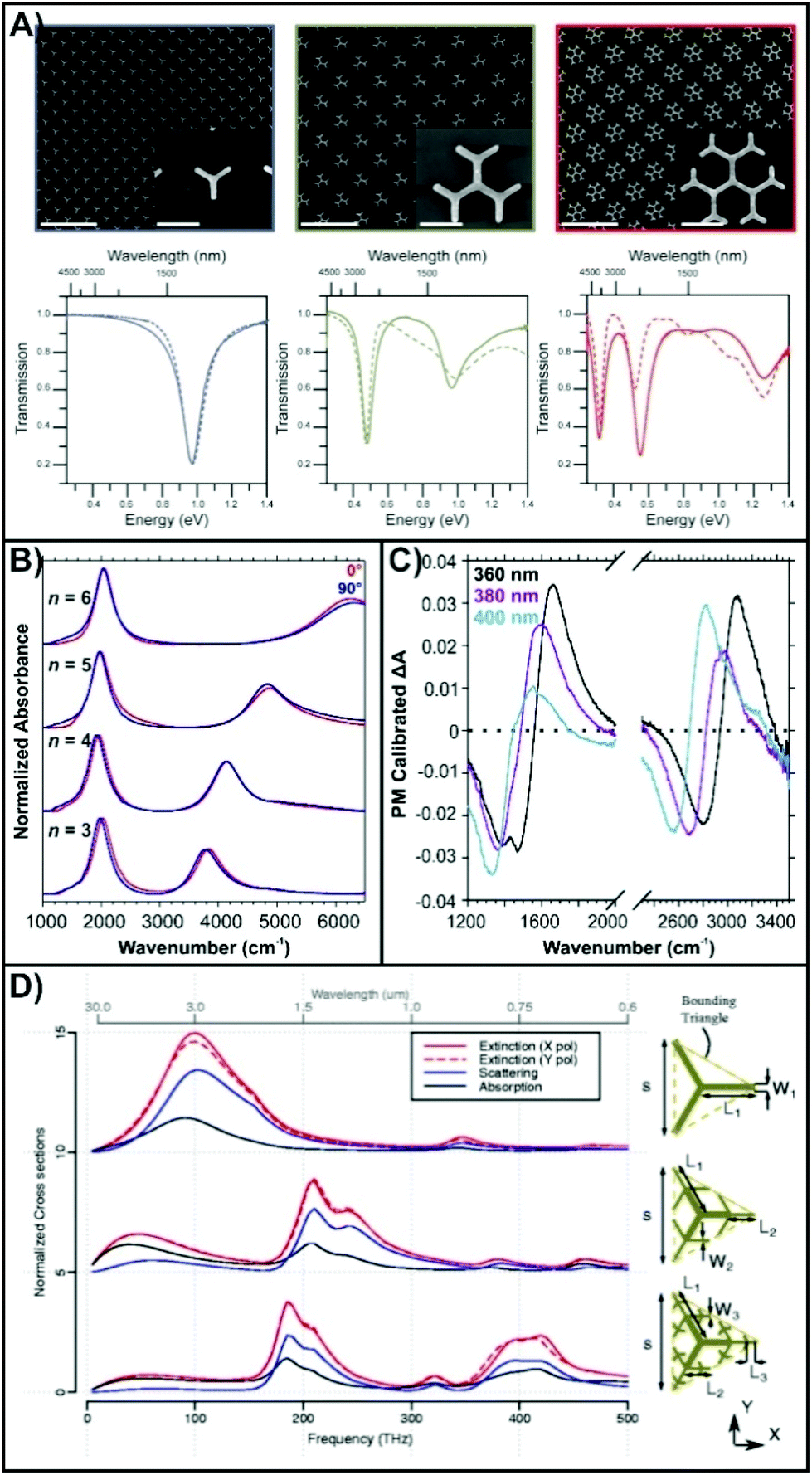 | ||
| Fig. 2 (A) SEM images and transmission measurements for three branched first-, second-, and third-order dendritic fractals.58 The scale bars in the array images are 2 μm, and 300 nm in the inset images. (B) Normalized absorbance spectra for second-order dendritic fractals with varying numbers of inner branches (n) using linearly polarized synchrotron light.59 (C) Calibration polarization modulated spectra for three branched second-order dendritic fractals with varying side lengths.60 (D) Spectral variation of the first through third-order generation Ternary tree fractal.61 Reproduced and adapted with permission from ref. 58–61. Copyrights 2015 and 2017 American Chemical Society, 2018 John Wiley and Sons, and 2016 Springer Nature respectively. | ||
Beginning with the generation order of the fractal, Fig. 2A shows that with each increase in the generation order, an additional resonance with lower energy is introduced. The nature of these resonances is discussed in greater detail later in this review. In short, the highest energy resonance encompasses only the outermost branches, while each lower energy resonances incorporates an additional generation of the fractal until the global (lowest energy) resonance is achieved. As shown in Fig. 2B, increasing the number of inner branches results in a blue-shift (shift to higher energy) of the resonances.59 This effect has been attributed to a change in the geometry of the fractal. As the number of branches increases, a greater amount of overlap is observed between the individual rods, resulting in less of the rods being exposed to the dielectric environment. Consequently, fractals with large numbers of inner branches (n = 6) exhibit greater shifts to the higher energy resonance, as clearly shown in Fig. 2B. By altering the dimensions and configurations of the fractal, it is possible to tune the spectral positions of the resonances to specific regions of the mid-IR spectrum. As a result, surface-enhanced measurements can be performed, as will be further explored in this review. Moreover, the fractals exhibit a polarization dependence (Fig. 2B) that can be exploited for other optical processes including polarization-modulation infrared linear dichroism microscopy (μPM-IRLD, Fig. 2C).60 The observed dichroic response (negative lobe to positive lobe) occurs at or very near to the position of the resonances. Depending on the design of the fractal, these dichroic responses differ. By introducing a molecule that exhibits a dichroic response to linearly polarized light to the surface of the fractal, it would be possible to probe this response at the monolayer level.
Multibranched structures, like that of a first-order generation dendrimer, have previously been prepared by EBL.52 These structures exhibited a resonance in the near-IR. However, it is unknown how the combination of generation order and the number of inner branches will influence the plasmonic properties in the visible to near-IR. Do the EBL dendrimers continue to exhibit a series of new intense resonances, or, is a single broad resonance (or continuum of resonances) observed? This question opens to valuable new insight into the nature of fractal plasmonics, including multispectral compatibility. Such a response has been proposed theoretically for the Ternary tree fractal (Fig. 2D),61 whereas opposed to branching outwards, the high-order generations branch inwards, with smaller dimensions than the previous generations. As a result, as opposed to lower energy resonances being introduced, higher energy resonances, closer to the near-IR and visible region are added. However, no experimental studies have been performed demonstrating the feasibility of fabricating such a structure, or how the structure can be used in different applications.
2.2 Sierpiński fractals
For the lithographically prepared dendrimers shown in Fig. 2, the fractal structure has a radial geometry. Alternatively, a base structure, or element, can be repeated such that larger structures with the same geometric shape are fabricated. These are known as Sierpiński-type fractals. For example, in a Sierpiński triangle,62–66 the base structure (zeroth-order generation) is an equilateral triangle. To form the first-order generation, the base triangles are arranged in a triangular shape, leaving a central cavity. This process is repeated for higher-order generations, leading to larger cavities with dimensions comparable to the size of the nanoprisms from the previous-order generation. An SEM image of a third-order Sierpiński triangle is shown in Fig. 3A.62 As the image also shows, as opposed to isolating the fractals, the fractals can be fabricated near each other forming a bow-tie assembly and maximize the EM enhancement at the small gap given the proper polarization. For the fractal structure, numerical calculations yielded resonances at ∼6300, 2700, and 1700 nm, with the extinction spectra remaining consistent below 1500 nm. Although the enhancement was lower, the calculated electric fields were enhanced even at a wavelength of 700 nm. As opposed to viewing the fractal as a build-up of smaller nanoprisms, the Sierpiński triangle can be fabricated by introducing the triangular nanocavities into a larger nanoprism. In doing so, a comparison between a solid nanoprism and the fractal generations with the same overall size can be made (Fig. 3B).65 When the nanoprisms within the bow-tie are subdivided, the dipolar resonance of the fractal shifts from ∼1700 nm for the nanoprism to ∼1900 nm for the first-order generation and to ∼2300 nm for the second-order generation. Such red-shifts were earlier observed at microwave frequencies,67 and have been observed in other studies involving plasmonic Sierpiński triangles.62,63 These shifts in resonance wavelengths are attributed to the introduction of additional modes that are the result of the nanocavities that are introduced upon fractalization. These interactions form the basis of the hybridization model and are discussed in greater detail in section 3. Other fabrication geometries include introducing a nanoscale spacing between the small nanoprisms within the fractal described as the open configuration in the inset image of Fig. 3C.65 By isolating the nanoprisms, no connections between adjacent structures are made, making the structure smaller, resulting in the resonance blue-shifting from 1900 nm to 1200 nm for the first-order generation structure. Expanding to higher-order generations will yield smaller nanoprisms yielding resonances in the visible to near-IR.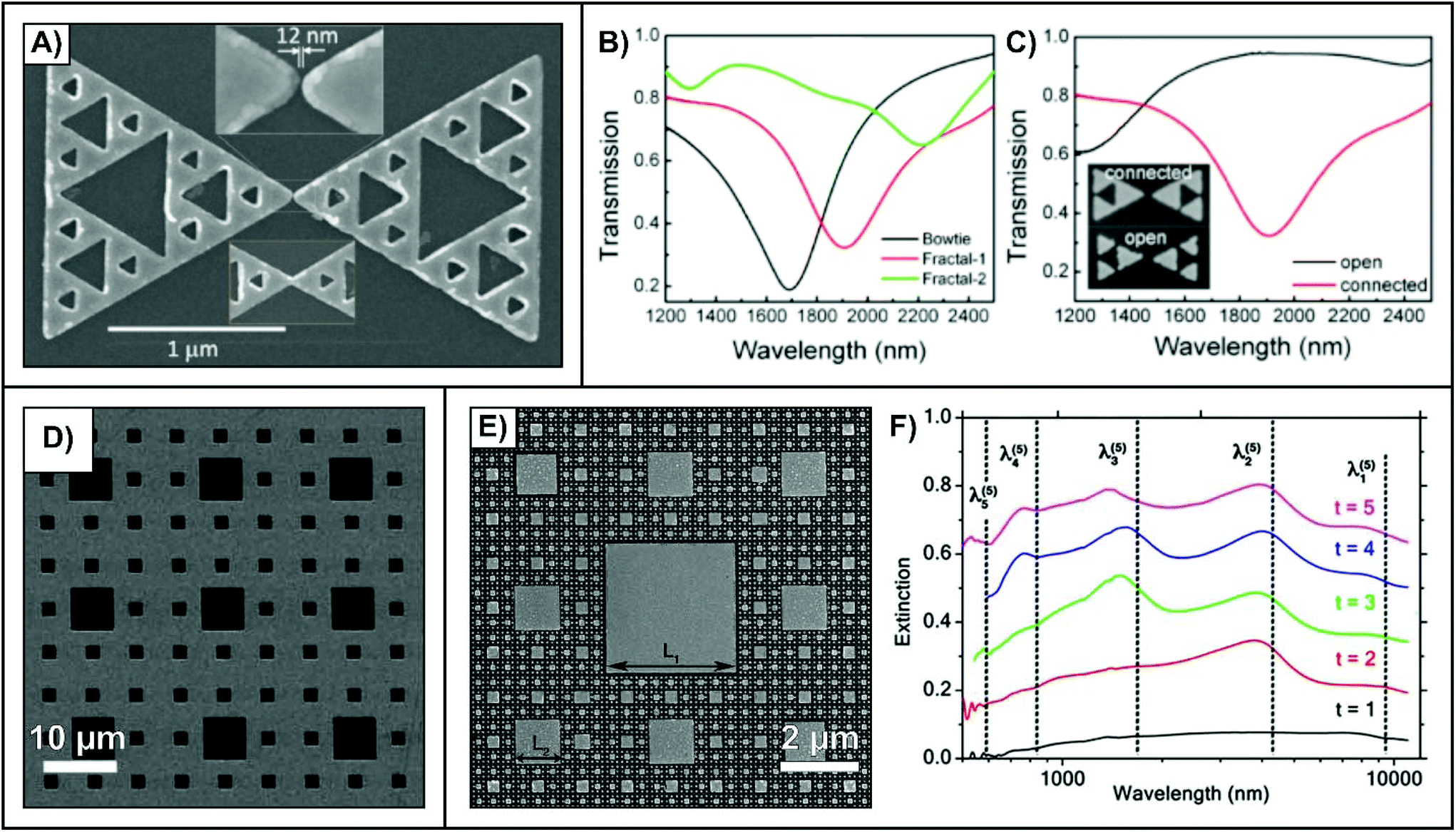 | ||
| Fig. 3 (A) SEM image of a third-order generation Sierpiński triangle.62 Transmission spectra comparing (B) nanoprism bowties, first- and second-order generation Sierpiński triangles and (C) Sierpiński triangles with open and connected nanoprisms.65 (D) SEM image of a gold thin film perforated with a Sierpiński carpet pattern.68 (E) SEM image of an inverted Sierpiński carpet with isolated nanostructures and (F) extinction spectra of the various fractal generations where t = 1 is just the large central structure and t = 5 is the fractal as shown E.75 Reproduced and adapted with permission from ref. 62, 65, 68, and 75. Copyrights 2011 John Wiley and Sons, 2014 Optical Society of America, 2008 AIP Publishing, and 2018 American Chemical Society respectively. | ||
If the elemental unit is a square, the resulting divergent-type fractal is known as a Sierpiński carpet,68–75 with other fractals such as the “center fractal” exhibiting structural similarities.76 In addition to EBL, Sierpiński carpets with nanocavities have been fabricated by focused-ion beam milling,72 and standard projection lithography (Fig. 3D).68 In the case of the shown fractal, as the structure is incorporated as a perforated film, only surface plasmon polaritons (SPP) were observed. Furthermore, due to the large dimensions of the fractal and the use of a silicon substrate the resonances were found to be in the mid- to far-IR (ω = 160, 223, 313, 348, 477, 664, 949, and 1047 cm−1). The introduction of nanostructures within the cavities was used to introduce LSPRs to the transmission spectra. In addition to solid films, like the Sierpiński triangle, isolated elemental structures can be used.72 Here, as the monomer unit had dimensions of 80 ± 8 nm, a broad resonance in the visible to near-IR (550–750 nm) was consistently observed.
An interesting alternative, one that has only somewhat applied to the Sierpiński triangle,66 is to fabricate the inverse structure. In such a configuration, what would normally be nanocavities become the isolated nanostructures, as demonstrated in Fig. 3E.75 Here, the side length of the introduced structure is 1/3 the side length of the structure from the previous generation. For the fifth-order generation fractal in Fig. 3E, the resulting structures have side lengths of 3.38, 1.12, 0.39, 0.13, and 0.044 μm from the first- through fifth-order generations respectively. With each new structure, an additional resonance at a shorter wavelength is observed in the extinction spectra (Fig. 3F). As the dimensions cover a wide range, the resonances span from the visible to the mid-IR. This approach of incorporating nanostructures with varying dimensions within the unit cell is analogous to studies involving metasurfaces that support multiple resonances in the mid-IR.77,78 The Sierpiński carpet has both advantages and disadvantages relative to the mentioned metasurfaces. Although it is possible to fabricate polarization insensitive metasurfaces,79 the resonances of the Sierpiński carpet are intrinsically polarization independent due to its centrosymmetric geometry. Furthermore, the basis of exhibiting broad optical properties is easily realized due to the iterative nature of the fractal. However, it is this same concept that makes tuning the resonances to specific wavelengths extremely challenging. In the case of traditional metasurfaces, the dimensions are individually tailored so that the resonances correspond to specific wavelengths. This is of importance for applications involving surface-enhanced infrared absorption (SEIRA)-based sensing. In the case of the Sierpiński carpet, since the dimensions of the structures are directly related, a high degree of tuning beyond a single wavelength is unlikely.
Given the nature of Sierpiński-type fractals, it is possible to extend the elemental geometry beyond triangles and squares to use other two-dimensional shapes (i.e. hexagons).80 To the best of our knowledge, no studies involving plasmonic nanostructures with such geometries have been published. Furthermore, as opposed to fabricating solid nanostructures, the base units can be subdivided into other structures. For example, the squares within the Sierpiński carpets can instead be made of four nanoprisms pointed inwards with a nanoscale gap separating them. Such a configuration would maintain the multiresonant nature of the fractal, while introducing a stronger enhancement of the EM at the apices located at the central gap. This improved EM enhancement could then be exploited for different applications.
2.3 Space-filling and similar fractals
In a planar space-filling curve, the range of the structure fits completely within a unit square. Geometries that fall within this category include but are not limited to: Peano,81 Peano-Gosper,82 Minkowski,83 Hilbert81,84,85 and the Sierpiński carpet.75 As shown in Fig. 4A for a Hilbert curve at a ninth-order generation,85 when fabricated by EBL the fractal is composed of continuous nanorods. There are several important features associated with these types of fractals. For a unit square with fixed dimensions, as the generation-order of the fractal increases, the dimensions of the constituent nanorods becomes smaller. Interestingly, unlike the constituent nanorods that are anisotropic, the overall fractal is isotropic. As such, there is no significant variation in the reflectance spectra when probed under orthogonal polarizations (Fig. 4B). Furthermore, the space between the nanorods becomes smaller as the order of the fractal increases. As a result, the reflectance spectra are “quasi-flat”, and resemble the optical response of a thin metallic film. However, a weak plasmon mode near 530 nm was observed. This was attributed to the finite width (50 nm) of the nanorods within the fractal. An earlier work involving Hilbert curves postulated that they could be used for surface-enhanced Raman spectroscopy (SERS).84 Given these results, it is unclear how effective such fractals would be for SERS. More work is needed both in exploring fractal-order and tuning the resonances before SERS experiments could be performed. Beyond working with the nanorod version of the fractal, it is also possible to use the curve to be the outer edge of a fractal structure. This approach was recently used to prepare Koch snowflake fractals that exhibit a series of resonances in the visible through mid-IR regions.86 Greater details regarding this fractal will be discussed later in this review.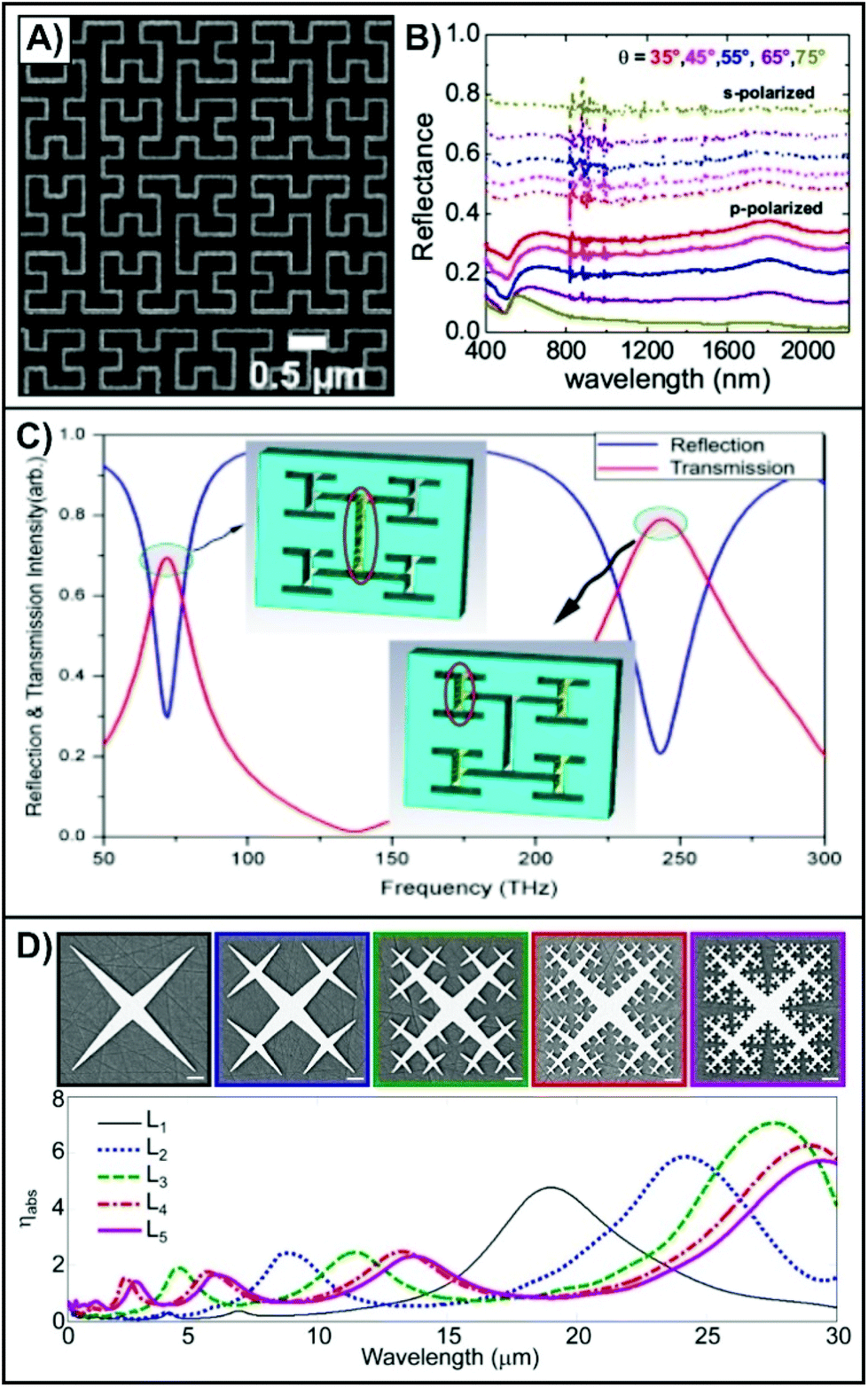 | ||
| Fig. 4 (A) SEM image of part of a ninth-order Hilbert fractal and (B) experimental reflectance spectra measured with p- and s-polarized light at varying angles of incidence.85 (C) Transmission and reflectance spectra of a perforated metallic film with an H-Tree fractal. The insets show the electric field distributions at the two resonances.87 (D) SEM images of different generations of Cesaro-type fractals and corresponding calculated absorption cross-section spectra.95 Reproduced and adapted with permission from ref. 85 and 95. Copyrights 2015 and 2016 American Chemical Society respectively. | ||
Although not a true space-filling fractal, structures with an “H” geometry, known as H-trees, are like the previously described curves. In a true H-tree fractal, with each new generation, the side length of the rods is √2 the length of the previous generation. However, decreasing the side length by ½ every other generation is more often used.87,88 Such a structure is shown in the inset diagrams of Fig. 4C.87 Much like the Hilbert curve of Fig. 4A, such an approach yields an isotropic structure. However, unlike the Hilbert curve, multiple modes are observed in the reflection/transmission spectra of a perforated metallic film with the H-fractal geometry.87 Here, the resonance at 73 THz (4107 nm) is attributed to the long slit of the first-order generation, and the resonance at 243 THz (1234 nm) is from the smaller slits in the third-order generation. As this study only went to the fourth-order generation, only two peaks were observed. The multiresonant nature of this fractal is analogous traditional dual-band perfect absorbers where the structure contains elements that are asymmetric or of different dimensions.89–92 Depending on the geometry, the resonances can be polarization dependent or independent. Regardless of this, the resonances are highly tuned to specific spectral domains of interest so that they can be used for specific applications, most notably SEIRA. To increase the number of resonances, yielding a multiband absorber, the fractal has to be expanded to higher-order generations.93 An interesting, and to the best of our knowledge unexplored approach, would be to use the mathematical H-tree design, where the side length differs with each generation. In such a design, the greater degree of variation in dimension would result in additional resonances, and the anisotropic nature would make the resonances polarization dependent. Such an approach could be of great value in the field of opto-electronics. Furthermore, given that nanorods and nanoslits have different polarization dependences,94 comparing H-tree fractals of both types could yield interesting and novel plasmonic properties.
Another quasi-space-filling fractal is the Cesaro-type fractal,95 where the overall size of the fractal is defined by the dimensions of the first-order generation. Much like the Ternary tree fractal described in the dendrimer section,61 as the fractal-order increases, pointed elements with the same geometrical motif are pointed inwards (Fig. 4D). By using sharp features, there is a stronger confinement of the local EM field at the extremity of the spikes. As the order of the fractal increases, two key spectral trends are observed. In the first-order generation, a single dominant mode at a wavelength of 18.7 μm was calculated. At the second-order generation, the resonance red-shifted to 23.7 μm. This trend of red-shifting the resonance was observed with each subsequent increase in the order of the fractal. The red-shift was attributed to the perturbation of the smaller branches that are introduced coupled with the overall increase in the effective length of fractal with each subsequent generation. Like the previous fractals, increasing the fractal-order introduces additional lower energy resonances. In the case of the fourth-order generation, the calculated absorbance spectra showed in Fig. 4D have four resonances (λ1 = 29 μm, λ2 = 12.9 μm, λ3 = 5.9 μm, and λ4 = 2.8 μm). The additional resonances are attributed to the spikes that are introduced in each new generation. As was the case for the dominant resonance, the newly introduced resonances red-shift with increasing generation. Given further tuning, namely by altering the dimensions of the spikes, these resonances could be finely tuned to specific wavelengths of interest. Of the fractals described in this section, the ability to have multiple resonances (as high as 5) over the entire surface of the fractal, that occupies an area less than 9 × 9 μm2 is incredibly advantageous. In this regard, it is comparable to the dendritic fractals in terms of supporting a large number of resonances in a small surface area. As such, it is believed that this type of structure will be relevant for many of the applications discussed later in this review.
3. Modelling and mapping the enhancement
Determining the spatial distribution of the EM enhancement for the various resonances of a nanostructure can provide insight into underlying cause of enhancement. This is especially important for fractal structures as the nature of the multiple resonances can be attributed to different structural elements or plasmonic principles. With a greater understanding of these effects, it becomes possible to design and fabricate structures with highly tailored plasmonic properties. For nanospheres, Mie's analytical solution to Maxwell's equations can be used to model the plasmonic properties of the structure.96 However, for more complicated geometries, such as fractals, numerical calculations are needed.97,98 In these calculations, the extinction spectra and spatial distribution of enhancement can be determined at the single-structure level.Examples of EM field calculations for three fractal structures are shown in Fig. 5. When the fractal geometry includes structures with different dimensions, such as an H-tree fractal, the EM field distribution of each resonance is very different (Fig. 5A).87 Consistent with what was predicted in the previous section for such a geometry, the long inner portion of the fractal has a resonance at a longer wavelength (λ = 4.11 μm), whereas the smaller arms of the fractal have a higher energy resonance (λ = 1.23 μm). As the arms of each generation are well separated, there is virtually no co-localization of the enhancement, that is overlap of the distribution at each resonance. Furthermore, the distinct distributions verify the multiresonant nature for this type of fractal. With each generation (or every other generation for a symmetric H-tree), smaller branches are introduced. These smaller branches will therefore support a different resonance at a higher energy than the previous one, with a different spatial distribution of EM enhancement. This effect is consistent across fractals structures and metasurfaces, where the size of the individual structures in each generation vary, as in the case of the Sierpiński carpet.
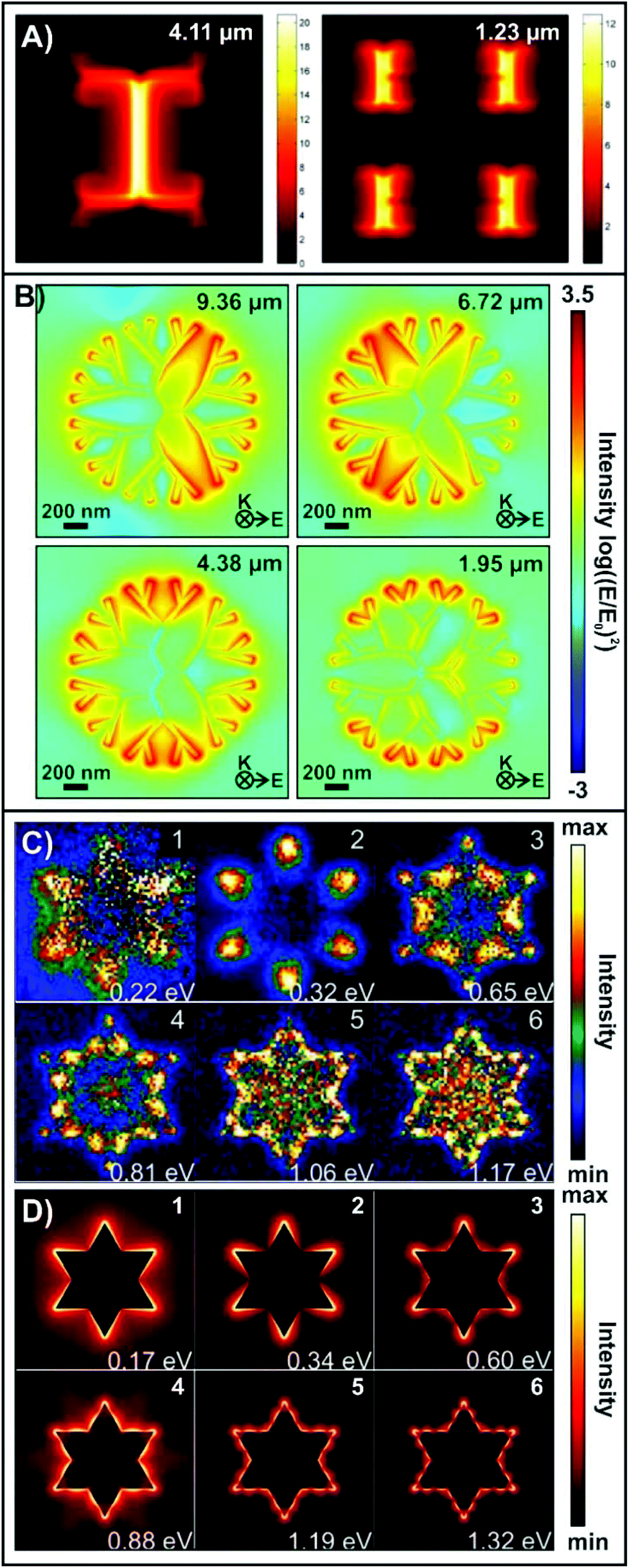 | ||
| Fig. 5 EM field distributions for (A) an H-tree fractal,87 and (B) a three-branched fourth-order generation dendritic fractals.59 (C) Experimental EELS maps and (D) corresponding calculated EM field maps for a first-order generation Koch fractal.86 Reproduced and adapted with permission from ref. 87, 59, and 86. Copyrights 2013 IOP Publishing and 2017 American Chemical Society respectively. | ||
For a dendritic fractal (Fig. 5B), each resonance exhibits a different overall distribution of enhancement, though there is overlap of enhancement between some of the resonances.59 At the lowest energy resonance (λ = 9.36 μm), the enhancement extends from the inner-most branches out towards the periphery. This resonance is therefore described as being the global LSPR of the structure. With each subsequent generation, branches from the inner portion of the fractals no longer exhibit enhancement, until only the outer dendrons are the source of the enhancement (highest energy resonance, λ = 1.95 μm). All the resonances were described as dipolar resonances. As the fractals can be fabricated with different symmetries,59,60 it is also possible to manipulate the distribution of enhancement by changing the polarization of the impinging light. To understand how the generation order of the fractal relates to the number of resonances and their spatial localization, a plasmon hybridization model was employed.99–101 The hybridization model was originally used to describe the origin of plasmon peak splitting in metallic nanoshells.99 In an approach that is analogous to molecular orbital theory, where the nanoshell can be viewed as a combination of a metallic sphere and a cavity with each of them supporting their own resonance. Due to the finite distance between the outer edges of the sphere and cavity, the plasmons interact with each other. The result of this interaction is the splitting of the plasmon resonance into two resonances: a lower energy symmetric or “bonding” plasmon and the higher energy antisymmetric or “antibonding” plasmon. This same description can be applied to the dendrimers as each generation can be described as a combination of the structures from the previous generation along with the structures that are to be introduced in the subsequent generation. Details regarding the tentative model used to describe the splitting for the dendritic fractals are in ref. 59.
It has been argued that a configuration where this is little to no overlap in EM enhancement at each resonance is less than ideal for sensing applications as different molecules would be detected at each hots-spot. In this regard, having a uniform distribution of the analyte over the surface becomes important.102 Comparing the results of Fig. 5A and B, the dendritic fractals would therefore be the preferable structure. It is necessary to note that before a final statement can be made, it is necessary to consider how the experiments are being performed. If the measurements are to be done at the single-structure level, where the size of the fractal is comparable to the beam diameter, then having co-localization of the enhancement will be important. However, if ensemble measurements are to be taken, then uniform distribution becomes less necessary as an average result is acquired. As such, we believe that overlap enhancement associated with different wavelengths is less important. Overall, we strongly believe that the relationship between the geometry of the fractal, the enhancement, and the nature of the experiment, must all be considered.
Due to the diffraction-limited nature of optical measurements, where the spatial resolution is limited to about λ/2 as defined by the Abbe criterion, experimentally probing the plasmonic properties at the single-structure level is quite complicated. One approach to probing the enhancement relies on the use of indirect measurements, where post-irradiation chemical transformations of a species adsorbed or spin-coated to the surface are probed by electron or scanning probe microscopy.103–105 These approaches however have not yet been applied to fractal nanostructures.
Electron energy loss spectroscopy (EELS) has recently been used to study the multiresonant nature of Koch snowflake fractals.86 Both the experimental EELS spectra for the first-order generation Koch fractal were found to have 6 resonances. The corresponding EELS map at the resonance wavelengths are shown in Fig. 5C. The lowest energy resonance (λ = 5.64 μm, 0.22 eV) was attributed to the overall dipolar mode of the Koch snowflake. As seen in the experimental (Fig. 5C) and calculated (Fig. 5D) EELS maps, the distributions are more complex. To understand this, the authors explored the edge geometry of the fractal, where two segments are placed with a 120° angle between them. In doing so, the authors determined that the remaining five modes of the fractal correspond to the different order modes of just the edges, with the second mode (λ = 3.87 μm, 0.32 eV) being the dipolar mode of the edge geometry. In the calculated EELS spectra, this mode was observed to be composed of two resonant modes separated by only 46 meV that could not be separated experimentally. Using a hybridization model, this splitting was attributed to the interaction of the edge dipolar modes. To further understand this interaction, a series of different edge lengths were simulated, where it was found that decreasing the side length resulted in a greater shift. This intrinsically makes sense as bringing the modes closer together (decreasing size) will lead to a greater interaction between the modes, and finally a larger splitting (as high as 1.2 eV) for the modes. This study highlights how experimental measurements coupled with numerical calculations can be used to explain complicated fundamental processes, such as plasmon mode interactions.
However, one of the challenges often associated with EELS measurements is the specific sample preparation requirements. In this regard, scanning probe microscopies could be a viable alternative as the measurements can be performed on the same sample used to acquire the far-field absorbance measurements. Here, the resolution is limited only by the apex of the tip used to scan the structures. Typically, these measurements are performed in the visible region and rely on techniques such as: tip-enhanced Raman spectroscopy,106 scanning near-field optical microscopy (SNOM),28 and scattering-type SNOM.107 Expanding into the infrared requires taking advantage of the advancements made in tunable mid-IR sources and combining the strong optical contrast that they provide with the high spatial resolution of an atomic force microscope. Such approaches have been applied to mid-IR compatible nanostructures.108–110 As many of the fractals described in this review, including those shown in this section, exhibit resonances in the mid-IR, we strongly believe that this approach will find use in studying fractal plasmonics.
4. Applications
4.1 Photovoltaics and photodetectors
The effectiveness of a solar cell is dependent on its ability to absorb incoming light and the collection of photocarrier current. There is an interest to switch from thick layer solar cells, to thin film solar cells. However, the decrease in thickness leads to a loss of the absorption of the intense light from 600–1100 nm within the solar spectrum.111 The interaction between light and metallic nanostructures has led to the preparation of plasmonic solar cells. The plasmonic nanostructures can be incorporated using colloidal lithography,112 where the power conversion efficiency improved from 3.82 to 4.57% for an organic thin-film solar cell when a mixture of different sized spheres was used. More recently, a power conversion efficiency of 29.2% was found for a simulated nanocorrugated perovskite solar cell, a large improvement from the 19.2% that was observed for a flat cell.113 Improving the efficiency of the solar cell by using plasmonic nanostructures is the result of several mechanisms including: (i) light scattering, (ii) near-field enhancement, (iii) plasmon-induced charge separation.8,114 Here, we will briefly discuss the role of the plasmonic nanostructures in these mechanisms to ascertain the potential role and interest of fractal structures in plasmonic solar cells. Metallic nanoparticles are known to efficiently scatter incident photons, with the scattering characteristics depending greatly on the particle geometry.115 The benefit of incorporating the nanoparticles is that the scattered light travels in all directions, and as a result, will travel longer distances through the active layer. This is especially important in thin-film devices as insufficient absorption due to transmission through thin active layer is a problem. A variety of different structures have been incorporated into plasmonic solar cells, with the ideal position within the cell dependent on the dimensions.116 In general, small nanostructures should be placed above the active layer as they preferentially scatter forwards, while larger structures predominantly scatter backwards and should therefore be added behind the active layer. Coupling both configurations together can be used to achieve greater efficiency.117 In that study, the top and bottom silver-based double plasmonic layers increased the absolute efficiency of ultrathin, flexible, upgraded metallurgical-grade polycrystalline silicon solar cells by 2.1 and 3.2% respectively. For a more in-depth comparison of the improved efficiencies exhibited when plasmonic nanostructures are added to solar cells, we encourage the reader to look at Tables 1–3 of ref. 114.To date, the incorporation of fractal structures, specifically Sierpiński carpet-like fractals, into solar cells has been modelled.73,74 In the first example,73 the silver structures have a thickness of 20 nm, and are placed on a 50 nm thin silicon film that is situated on a 250 nm thick silver contact (schematic in Fig. 6A). By itself, the free-standing silicon film was found to have a quantum efficiency of 3.16% (ref-1 in Fig. 6A). By introducing the silver contact, the quantum efficiency was improved to 6.55% (ref-2 in Fig. 6A). The authors then calculated how the individual nanocuboids of the fractal influence the efficiency (P1–3 in Fig. 6A), followed by the effect of the complete fractal. On its own, a quantum efficiency of 12.05% was achieved for the fractal. This yields a respectable improvement of 5.50%. However, it was found that the reflectance from 480 to 670 nm was very high, and the absorbance very low. To lessen this, a 100 nm thick layer of SiO2 was added to act as an antireflection coating (ARC). By adding the ARC, the quantum efficiency was further improved to 14.22%. In an alternative approach,74 the Sierpiński carpet made with silver nanocuboids of 50 nm thickness, were added to the silver back contact (Fig. 6B). To the patterned back contact, a 200 nm thick layer of silicon, followed by an 80 nm antireflective layer of Si3N4 was added. Much like the previous example, the addition of the fractal surface increased the absorbance of the light (green spectrum in Fig. 6C). Because of adding the fractal metasurface, a 109% increase of the short-circuit current density was calculated.
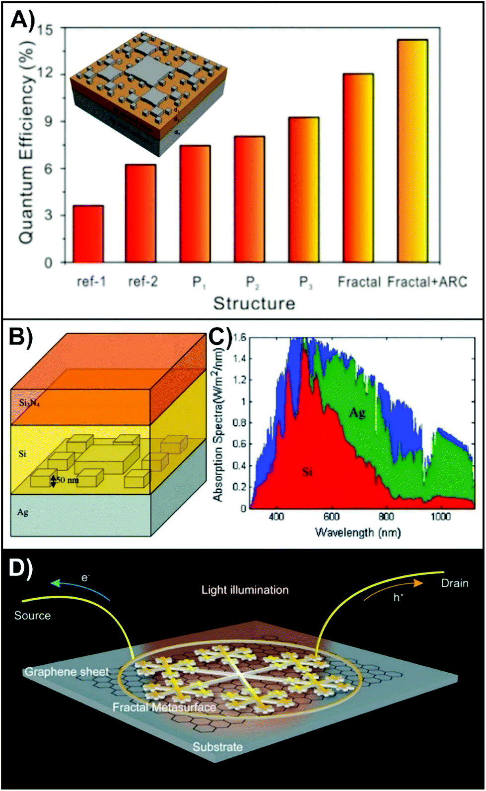 | ||
| Fig. 6 (A) Calculated quantum efficiencies of the 50 nm thick silicon solar cells with and without any plasmonic structures on top of the silicon layer, as shown in the inserted schematic. The highest efficiency incorporates an anti-reflective coating (ARC).73 (B) Schematic of solar cell with plasmonic nanoridges on the silver back contact and (C) the calculated absorbance spectra of the solar cell (red and green) with respect to the incident solar spectrum (blue).74 (D) Schematic representation a metal–graphene–metal photodetector using a gold snowflake-like fractal metasurface.122 Reproduced and adapted with permission from ref. 73, 74, and 122. Copyrights 2013 Optical Society of America, 2014 Springer Nature, and 2017 American Chemical Society respectively. | ||
Although such calculated results do show promise for improving the efficiency of solar cells by adding fractals, no solar cells have been fabricated where lithographically prepared fractals were incorporated. The challenge is not one of fabrication capability, but of practicality. EBL is a technique of choice for preparing fractal structures, but it is hindered in its inability to prepare the structures over large areas in a rapid manner. Given that other fabrication processes can provide the necessary high-throughput capabilities for solar cells, we believe that exploring how the methodology effects the structural and optical properties of the fractal is a possible area of future research. In some cases, three-dimensional (as opposed to pseudo-planar) structures can be prepared.118 Perhaps by using these other methods/structures, the introduction of fractal metasurfaces can be achieved.
Beyond improving the light–matter interactions with solar cells, plasmonic nanostructures have also found use for improving graphene based opto-electronics including photodetectors.119–122 Graphene's unique opto-electronic properties, notably the zero-band gap and ultrahigh carrier mobility, has made it an interesting alternative to traditional semiconductor compounds that often contain environmentally harmful elements (i.e. arsenic and mercury).123 However, due to the low light absorption (∼2.3%) of the atomic thickness of graphene,124 and the ultrashort lifetime of photoinduced carriers,123 photodetectors based solely on the use of graphene are limited. Like solar cells, graphene-based photodetectors can benefit from the enhanced optical absorption and the generation of electron–hole pairs. The generated carriers are then separated at the gold–graphene interface, yielding a detectable photovoltage. This was the approach that was used in a recent study involving a metal–graphene–metal photodetector, where the plasmonic nanostructures were gold snowflake-like fractals (Fig. 6D).122 As we have thoroughly described in this review, the advantage in using fractal nanostructures is that they support broadband plasmonic properties. Here, the emphasis was once again placed on the visible region, with enhancement factors ranging from 8–13, though the concept could be expanded to other spectral domains. Furthermore, due to the opto-geometric properties of the fractal, this enhancement was polarization insensitive, a key design requirement for photodetectors.
4.2 Refractive index sensing
The spectral position of plasmon resonances depends on the opto-geometric and material properties of the nanostructure, and the refractive indices of the substrate and surrounding media. As the refractive index of either the substrate or surrounding media increases, the resonances undergo a red-shift.125 Changing the refractive index of the substrate can enable the resonance position to be tuned for vibrational spectroscopy,126 whereas the surrounding media can be used for refractive index sensing. This is often referred to as SPR and LSPR sensing. These techniques have shown significant promise for clinical biosensors and medical diagnostics due to the high sensitivity that it has at the monolayer level.127 For example, the resonance for arrays of gold nanoprisms at 973.0 nm underwent a 31.5 nm red-shift after surface modification, followed by a subsequent 10.0 nm red-shift after exposure to the bacteria Pseudomonas aeruginosa.128 The developed process was sensitive enough to detect the shift associated with the binding of a single bacterium. As opposed to working with “positive” structures (i.e. nanoprisms), “negative” structures (i.e. nanoholes) can also be used. Extraordinary optical transmission (EOT) relies on the use of platforms composed with arrays of structured nanoapertures in an optically thin metallic film.129 Like SPR and LSPR sensing, the change in the refractive index at the metal surface results in a peak shift in the EOT spectrum. The advantage of developing fractal structures for refractive index-based sensing is the presence of multiple resonances in the spectra. Thus far, the incorporation of fractals to these processes has emphasized “negative” fractals, as shown in Fig. 7A, with resonances in the near- to mid-IR (THz region as described in Fig. 7).66,130–132 As shown in Fig. 7B, when the media surrounding the fractal is altered, the resonances undergo linear shifts (Fig. 7C).130 As conventional biomaterials have different refractive indices, (ether, 1.35; ethylene glycol, 1.43; chlorobenzene, 1.52; quinoline, 1.62), these materials can be used to evaluate the shifts associated within small increases in the refractive index (Fig. 7D).132 Once again, the presence of multiple peaks provides an opportunity for greater sensitivity for measuring the small shifts.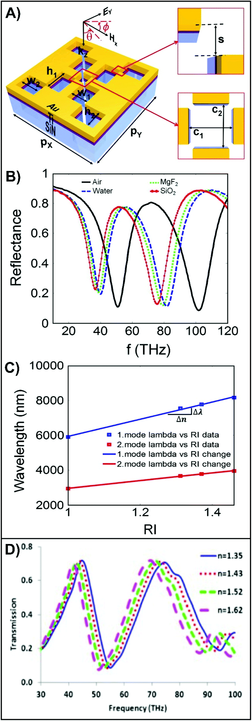 | ||
| Fig. 7 (A) Schematic of the rectangular fractal nanoaperture. (B) Calculated reflectance spectra of a rectangular fractal nanoaperture surrounded by different cladding media and (C) the refractive index sensitivity of the structure for the cladding media.130 (D) Calculated transmittance spectra of meandered cross nanoapertures coated with graphene at a potential of 0.2 eV and surrounded by biomaterials with different refractive indices.132 Reproduced and adapted with the permission of ref. 130 and 132. Copyrights 2015 and 2017 Elsevier respectively. | ||
The presence of multiple resonances that have the potential to span different spectral domains is the greatest advantage of fractal structures to refractive index sensing. Furthermore, Fig. 7B highlights that the linear responses can differ for each resonance. This is especially beneficial when attempting to trying to relate the changes in refractive index to the detection of an analyte. The response from each resonance can be viewed individually, and the concentration of the analyte determined. By comparing the values determined for each resonance, a greater accuracy can be achieved for the reported concentration. Although the highlighted results are promising for the development of the field, it is necessary to recognize that these results are predominantly calculated as opposed to experimental and focus on bulk media and thin films instead of monolayers. Given that these techniques have shown monolayer sensitivity for classical structures, we strongly believe that the fractals will achieve the same results. As well, consistent with the literature on lithographically prepared fractals, the focus has been on the mid-IR. Given that SPR, LSPR, and EOT-based sensing use visible and near-IR light, more work should probe fractals with resonances in those regions to maintain consistency with the existing approaches. Incorporating the fractal structures with sensor geometries that have shown improved sensing performance, such as coupled cavities and nanostructures,133 is another area of possible focus as this could improve the figure-of-merit of the shown sensing platforms.
4.3 Surface-enhanced spectroscopies
Surface-enhanced spectroscopies including Raman (SERS), fluorescence (SEF), and infrared absorption (SEIRA) rely on the use of metallic nanostructures. Several recent reviews have been published about these techniques,102,134–138 ranging from the fundamentals to their applications. The use of fractal-like structures for SERS dates back to the 1980s.41 Since then, a variety of fractal and fractal-like geometries have been applied to SERS, though here we are most interested in the use of lithographically prepared fractals as these have been the primary focus of this review.65,69,75,84,139,140 As the SERS responses of such structures are still being evaluated, most studies employ the use of molecules with large Raman scattering cross-sections, as shown in Fig. 8A for Sierpiński carpets coated with brilliant cresyl blue that is electronically resonant under 633 nm excitation.75 In the case of the Sierpiński carpet, only the smallest structures (introduced at the higher-order generations (t = 5)) yield significantly greater responses than the reference Au film. This is because the resonance(s) in the visible region are attributed to the smaller structures (side length = 44 ± 3 nm), whereas the larger structures have resonances in the near- to mid-IR. By mapping the integrated SERS intensity of a peak, it is possible to relate the geometry of the fractal (Fig. 8B) to the observed SERS response (Fig. 8C).69 This approach can be used to experimentally show spatial distribution of the enhancement over the surface of the fractal. In the case of Fig. 8C, the regions with the smaller nanostructures yield a stronger signal (green) than the larger structures (black). Beyond fundamental studies, fractals can also be used for SERS-based sensing experiments. Here, we highlight the recent work of Lafuente et al. where a three-dimensional fractal was fabricated by a combination of anisotropic Si-etching, corner lithography, and self-assembly of gold nanoparticles.140 This fractal was then applied to the gas phase detection of dimethyl methylphosphonate (DMMP). DMMP is used in SERS studies interested in the detection of chemical warfare agents as it is a chemical simulant to sarin.141–145 The SERS spectrum obtained at the top of the three-dimensional fractal (Fig. 8D) has two distinct signals at 706 and 780 cm−1 corresponding to the P–C stretching and PO2 bending modes respectively obtained with an acquisition time of 1 second.140 As the interaction between the DMMP and the citrate of the gold nanoparticles is reversible, purging with N2 for 25 minutes is sufficient for the DMMP signal to disappear, thus yielding a reusable SERS substrate.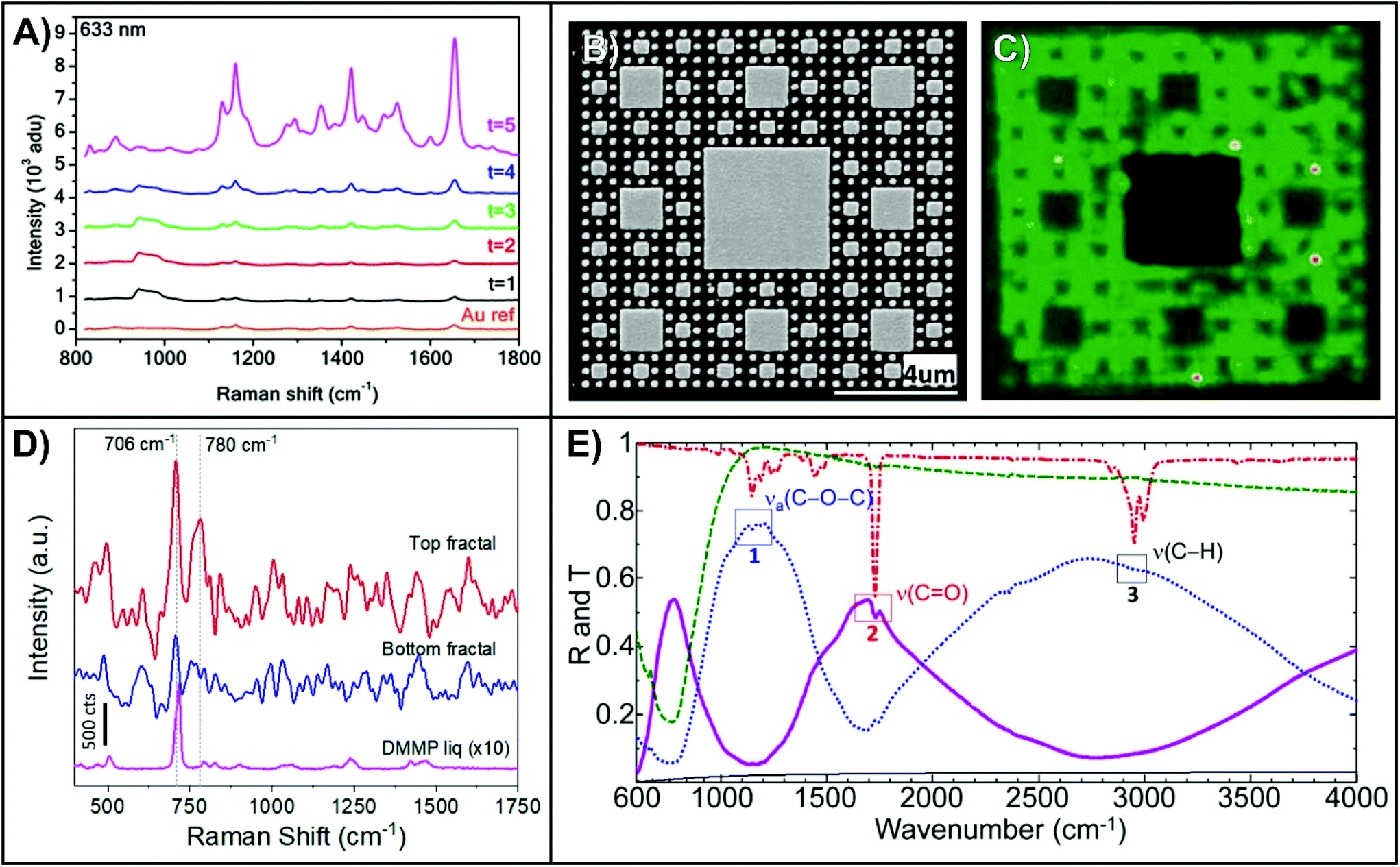 | ||
| Fig. 8 (A) SERS spectra of brilliant cresyl blue coated Sierpiński carpets for first- through fifth-order generations and a reference Au film.75 (B) SEM image of a fourth-order Sierpiński carpet and (C) SERS map of a cyanine dye adsorbed onto an Al2O3 layer deposited onto the silver fractals.69 (D) SERS spectra of a 3-dimensional fractal exposed to dimethyl methylphosphonate (DMMP).140 A normal Raman spectrum of DMMP in liquid is included for comparison. (E) Reflectance (solid purple line) and transmittance (dashed blue line) SEIRA spectra of PMMA coated fifth-order generation Cesaro-type fractal.95 Reflectance (solid black line) and transmittance (dashed green line) of a 10 nm thick layer of PMMA on CaF2 and reflectance (red dashed line) spectrum of a gold film coated with a 600 nm thick layer of PMMA are included for reference. Reproduced and adapted with the permission of ref. 95, 75, 69, and 140. Copyrights 2016 and 2018 American Chemical Society, 2010 Wiley and Sons, and 2018 MDPI respectively. | ||
Developing structures that exhibit compatibility with SEIRA is more challenging than SERS. In SERS, a general approach to achieving enhancement is to tune the maximum of the plasmon resonance so that it is between the desired excitation wavelength and the Raman frequencies.146,147 In a more nuanced approach designed to maximize the SERS enhancement, it is also necessary to consider the amount of spectral shift that exists between the observed LSPR position and the position of maximum near-field enhancement.148 When working with longer wavelengths, this effect becomes more pronounced and should therefore be considered. Regardless of whether the general or nuanced approach to tailoring the LSPR position is used, since the Raman scattered photons have a wavelength that is marginally shifted relative to the excitation wavelength, enhancement over the entire fingerprint region can be achieved without using overly broad LSPRs. In SEIRA, it is necessary to have a resonance(s) that span a broad spectral region (1000–4000 cm−1, 2.5–10 μm) or a series of resonances tuned to specific domains of interest. This is often achieved using tailored dual-band perfect absorbers and metasurfaces.77–79,89,90,149 Alternatively, fractal nanostructures can be used to achieve resonances compatible with SEIRA measurements.59,60,95,150 For example, Fig. 8E depicts SEIRA spectra obtained using a fifth-order generation Cesaro-type fractal coated with a 10 nm layer of poly(methyl methacrylate) (PMMA).95 Using both reflectance and transmittance measurements, characteristic vibrational modes of PMMA (as indicated in Fig. 8E) were observed. Specifically, the asymmetric C–O–C stretching modes between 1150–1250 cm−1, C![[double bond, length as m-dash]](https://www.rsc.org/images/entities/char_e001.gif) O stretching mode at 1732 cm−1, and C–H stretch combination mode between 2952–2922 cm−1. For a nanorod-derived metasurface to achieve the same results, it would need to be fabricated with nanorods of three different dimensions. As we have described, the mid-IR resonances of fractal structures can be tuned depending on the fractal shape and geometry. SEIRA has found itself to be an effective technique for biosensing, with the current challenge being to prepare structures and metasurfaces that exhibit resonances between 1500–1700 cm−1 and 2800–3000 cm−1 as these regions correspond to the amide and CH2 bands respectively.78 To the best of our knowledge, no studies involving fractal structures have explored this application, though the fractals used for SEIRA either already have or could be designed to have the resonances in those spectral domains.59,60,95,150
O stretching mode at 1732 cm−1, and C–H stretch combination mode between 2952–2922 cm−1. For a nanorod-derived metasurface to achieve the same results, it would need to be fabricated with nanorods of three different dimensions. As we have described, the mid-IR resonances of fractal structures can be tuned depending on the fractal shape and geometry. SEIRA has found itself to be an effective technique for biosensing, with the current challenge being to prepare structures and metasurfaces that exhibit resonances between 1500–1700 cm−1 and 2800–3000 cm−1 as these regions correspond to the amide and CH2 bands respectively.78 To the best of our knowledge, no studies involving fractal structures have explored this application, though the fractals used for SEIRA either already have or could be designed to have the resonances in those spectral domains.59,60,95,150
One possible limitation of the current fractal geometry designs is that the reported enhancement factors are typically in the lower range of the often-reported values of 104–108 for SERS and 102–105 for SEIRA.102,151,152 For the lithographically prepared fractals, the SERS enhancement factors commonly ranged from 104–105,65,75,140 whereas the synthetic dendrimers offered up to an additional order of magnitude of enhancement.43–45 In three of these studies, comparisons were made with non-fractal structures: gold nanoparticles on a silver mirror,140 gold bowtie assemblies,65 and a commercially available SERS substrate.44 When compared, each study found that the fractals out-performed the non-fractal structure. The EM enhancement factors reported in the SEIRA studies ranged from 103–104,59,60,95,150 comparable to studies involving dual-band perfect absorbers and metasurfaces.77–79,89,90 Furthermore, these enhancements were also comparable to those of nanorods,23,94 one of the more common structures for SEIRA experiments including biosensing.78,153,154
With these values in mind, we propose two design features that could be used to improve the enhancement for SERS and/or SEIRA. A general approach would be to fabricate the structures on substrates that have a metal film with a dielectric layer on top of it. For lithographically prepared structures, these on-mirror-like configurations have previously been used to improve both SEIRA and SERS enhancement by one to two orders of magnitude.155,156 Another approach is to fabricate the fractals with base units that are near each other. This is due to the enhanced coupling that occurs when the gap between adjacent structures is less than a hundredth of the excitation wavelength.157 The inverted Sierpiński-type fractals (Fig. 8B) are especially well-suited to this approach as the fractals are designed to have a spacing between adjacent structures and generations. In other cases, the base unit of the fractal could instead be prepared as a series of smaller structures with nanoscale gaps between them. Such a design could be more readily adapted to fractals composed of linear arrangements of nanorods (i.e. H-tree). It was demonstrated that combining both design elements with a highly tuned structure, a SEIRA enhancement factor of 107 can be achieved.158 Overall, it is important to recognize that a lower initial enhancement factor may become less of an issue once all elements of the plasmonic device are considered and optimized.
4.4 Correlative measurements
As the spectroscopic information obtained by SERS and SEIRA can be complimentary, developing nanostructures and metasurfaces compatible with both techniques is of interest for sensing applications. In addition, the sensitivities of SERS and SEIRA both in enhancement and enhancing volume are different. For typical SERS structures, enhancement factors of 104–108 are reported,151,152 while for SEIRA, these values are typically lower (102–105).102 However, SERS is typically only sensitive to the first few nanometers above the surface,159,160 though the sensitivity can be extended beyond this limit.161,162 Whereas SEIRA enhancement extends 10's of nanometers above the structures.153 Therefore, performing subsequent SERS and SEIRA measurements can provide valuable spectroscopic information about complex molecular systems. To perform correlative measurements, it is necessary that the nanostructure, metasurface, or platform exhibit broad resonances or series of resonances in the visible and mid-IR. Approaches for having broader resonances include the use of clusters of nanostars,163 and ordered nanoparticle arrays,164,165 nanocomposites composed of multiple materials,166,167 and hierarchical structures.168 More relevant to the field of fractal plasmonics are structures and metasurfaces that have a series of highly tuned resonances. For single structures, these resonances can be polarization dependent (nanorods),27 or polarization independent (logarithmic antennas).31 We have previously demonstrated that a platform composed of superimposed arrays of nanoprisms with varying dimensions can provide the necessary multispectral compatibility for correlative measurements.35 For example, the Sierpiński carpet fabricated by De Nicola et al. meets such a requirement as at the fifth-order generation there are five resonances between the visible and mid-IR.75 However, to the best of our knowledge, no such correlative experiments have been performed with fractal structures. This therefore serves as a field of possible interest for future sensing studies involving fractal structures.In addition, SPR/LSPR measurements can be coupled with vibrational spectroscopy. Doing so provides chemical information about the adsorbed species while maintaining the label-free nature of SPR/LSPR sensing. To this end, experiments involving probing the spectral shifts along with either SERS,169 surface-enhanced near-infrared absorption,170 or SEIRA measurements have been performed.171,172 Although these methods can require varying instruments, we believe that performing subsequent measurements, as in the case of SPR/LSPR and SERS, can provide validation of the experiment. Here, SPR/LSPR sensing would be used for the analytical detection, while SERS would provide information about the analytes themselves. As we have described throughout this review, the advantage of fractal nanostructures are the broad optical properties. With sufficient development, a single fractal structure or metasurface could be used for optical processes in the visible through mid-IR. As a result, nearly any spectroscopic measurement could be performed either on its own, or as we recommend, in tandem with another.
5. Outlook
By using computer design and modelling, it has become easier to design fractals with a variety of geometries. The challenge then becomes to select the ideal dimensions so that the plasmonic properties are at the wavelengths or spectral domains of interest. To this end, using numerical calculations can provide critical information about the plasmonic properties of the structure before fabrication. These calculations also provide valuable insight into the nature of those properties, such as the origin of the multiresonant nature that fractal structures have become synonymous with. Once a configuration along with a range of dimensions and geometries have been decided upon, advanced nanofabrication techniques can then be used to prepare the structures with nanoscale precision. Throughout this review, we have highlighted examples for a variety of fractal geometries. This is by no means an exhaustive list of all possible designs. The work of Benoit Mandelbrot can help to serve as inspiration for future structures for fractal plasmonics.36 Furthermore, given that the field of fractal plasmonics began by adapting existing structures with properties in the GHz range, we believe that this concept of adapting geometries will continue. Whether it is from long wavelengths to short wavelengths or vice versa, tailoring the optical properties to specific domains of interest is application specific.As we have demonstrated, like traditional plasmonic nanostructures, fractal geometries can be applied to a variety of applications ranging from plasmon-mediated sensing to solar cell technologies. However, this is also the area that we believe will see the greatest amount of growth in the future. With a greater understanding of the plasmonic properties comes the ability to seek out a greater number of applications. Driving chemical reactions at the metal surface is one such application.173,174 By utilizing fractal geometries, a variety of excitations wavelengths and sources could be used. A significant advantage could be the use of white light sources to perform the reactions assuming that the fractal supports broad properties in the visible region, as is also associated with plasmonic solar cells. Simultaneously, the reaction progress could be monitored by using plasmon-mediated spectroscopy, either using visible or infrared light. Depending on the nature of the chemistry performed, techniques such as multiplexing measurements where multiple analytes are introduced could be performed.7,103 Beyond designs and applications, the next steps include integration into devices. In the case of sensing, given the use of advanced nanofabrication, microfabrication can be subsequently used to perform measurements involving microfluidics.175,176 Like the broadband nature of the fractals themselves, fractal plasmonics has emerged as a field of interest for a broad range of scientific and engineering disciplines and has the potential to widely grow. From fundamental developments in structures and optical properties, to the use of different techniques, and exploiting them for a variety of applications, fractals plasmonics has successfully emerged as an important sub-field in the ever-expanding field of nanoscience.
Conflicts of interest
There are no conflicts to declare.Acknowledgements
This research was supported by the Natural Sciences and Engineering Research Council (NSERC) of Canada. This research was further funded by the Canada Research Chairs program in “Photonics and Nanosciences” (F. L.-L.).References
- X. Ren, E. Cao, W. Lin, Y. Song, W. Liang and J. Wang, RSC Adv., 2017, 7, 31189–31203 RSC.
- C. H. Choi, K. Chung, T.-T. H. Nguyen and D. H. Kim, ACS Energy Lett., 2018, 3, 1415–1433 CrossRef CAS.
- A. Kumar, S. Kim and J.-M. Nam, J. Am. Chem. Soc., 2016, 138, 14509–14525 CrossRef CAS PubMed.
- J. Li, J. Liu and C. Chen, ACS Nano, 2017, 11, 2403–2409 CrossRef CAS PubMed.
- M. Nguyen, I. Kherbouche, S. Gam-Derouich, I. Ragheb, S. Lau-Truong, A. Lamouri, G. Lévi, J. Aubard, P. Decorse, N. Félidj and C. Mangeney, Chem. Commun., 2017, 53, 11364–11367 RSC.
- P. J. Straney, N. A. Diemler, A. M. Smith, Z. E. Eddinger, M. S. Gilliam and J. E. Millstone, Langmuir, 2018, 34, 1084–1091 CrossRef CAS PubMed.
- S. Simoncelli, Y. Li, E. Cortés and S. A. Maier, ACS Nano, 2018, 12, 2184–2192 CrossRef CAS PubMed.
- K. Ueno, T. Oshikiri, Q. Sun, X. Shi and H. Misawa, Chem. Rev., 2018, 118, 2955–2993 CrossRef CAS PubMed.
- Z. Zhang, H. Wang, Z. Chen, X. Wang, J. Choo and L. Chen, Biosens. Bioelectron., 2018, 114, 52–65 CrossRef CAS PubMed.
- S. Laing, L. E. Jamieson, K. Faulds and D. Graham, Nat. Rev. Chem., 2017, 1, 0060 CrossRef CAS.
- S. Xu and Y. Lei, ChemPlusChem, 2018, 83, 741–755 CrossRef CAS.
- T. Xie, C. Jing and Y.-T. Long, Analyst, 2017, 142, 409–420 RSC.
- A. M. Watson, X. Zhang, R. Alcaraz de la Osa, J. M. Sanz, F. González, F. Moreno, G. Finkelstein, J. Liu and H. O. Everitt, Nano Lett., 2015, 15, 1095–1100 CrossRef CAS PubMed.
- B. Wu, J. Lee, S. Mubeen, Y.-S. Jun, G. D. Stucky and M. Moskovits, Adv. Opt. Mater., 2016, 4, 1041–1046 CrossRef CAS.
- B. Cerjan, X. Yang, P. Nordlander and N. J. Halas, ACS Photonics, 2016, 3, 354–360 CrossRef CAS.
- T. H. Tan, J. Scott, Y. H. Ng, R. A. Taylor, K.-F. Aguey-Zinsou and R. Amal, ACS Catal., 2016, 6, 8021–8029 CrossRef CAS.
- P. Verma, Y. Kuwahara, K. Mori and H. Yamashita, J. Mater. Chem. A, 2016, 4, 10142–10150 RSC.
- K. N. Kanipe, P. P. F. Chidester, G. D. Stucky, C. D. Meinhart and M. Moskovits, J. Phys. Chem. C, 2017, 121, 14269–14273 CrossRef CAS.
- S. Tian, O. Neumann, M. J. McClain, X. Yang, L. Zhou, C. Zhang, P. Nordlander and N. J. Halas, Nano Lett., 2017, 17, 5071–5077 CrossRef CAS PubMed.
- J. Asselin, M.-P. Lambert, N. Fontaine and D. Boudreau, Chem. Commun., 2017, 53, 755–758 RSC.
- Q. Ding, M. Chen, Y. Fang, Z. Zhang and M. Sun, J. Phys. Chem. C, 2017, 121, 5225–5231 CrossRef CAS.
- D. Rodrigo, A. Tittl, O. Limaj, F. J. García de Abajo, V. Pruneri and H. Altug, Light: Sci. Appl., 2017, 6, e16277 CrossRef CAS PubMed.
- M. Tzschoppe, C. Huck, J. Vogt, F. Neubrech and A. Pucci, J. Phys. Chem. C, 2018, 122, 15678–15687 CrossRef CAS.
- F. D'apuzzo, M. Esposito, M. Cuscunà, A. Cannavale, S. Gambino, G. E. Lio, A. De Luca, G. Gigli and S. Lupi, ACS Photonics, 2018, 5, 2431–2436 CrossRef.
- S. Bagheri, N. Strohfeldt, M. Ubl, A. Berrier, M. Merker, G. Richter, M. Siegel and H. Giessen, ACS Photonics, 2018, 5, 3298–3304 CrossRef.
- J. S. Biggins, S. Yazdi and E. Ringe, Nano Lett., 2018, 18, 3752–3758 CrossRef CAS PubMed.
- C. D'Andrea, J. Bochterle, A. Toma, C. Huck, F. Neubrech, E. Messina, B. Fazio, O. M. Maragò, E. Di Fabrizio, M. Lamy de La Chapelle, P. G. Gucciardi and A. Pucci, ACS Nano, 2013, 7, 3522–3531 CrossRef PubMed.
- A. Garreau, M. Tabatabaei, R. Hou, G. Q. Wallace, P. R. Norton and F. Lagugné-Labarthet, J. Phys. Chem. C, 2016, 120, 20267–20276 CrossRef CAS.
- J. Song and W. Zhou, Nano Lett., 2018, 18, 4409–4416 CrossRef CAS PubMed.
- W. Wei, N. Chen, J. Nong, G. Lan, W. Wang, J. Yi and L. Tang, Opt. Express, 2018, 26, 16903–16916 CrossRef PubMed.
- H. Aouani, M. Rahmani, H. Šípová, V. Torres, K. Hegnerová, M. Beruete, J. Homola, M. Hong, M. Navarro-Cía and S. A. Maier, J. Phys. Chem. C, 2013, 117, 18620–18626 CrossRef CAS.
- K. Thyagarajan, J. Butet and O. J. F. Martin, Nano Lett., 2013, 13, 1847–1851 CrossRef CAS PubMed.
- J. A. Bossard, L. Lin, S. Yun, L. Liu, D. H. Werner and T. S. Mayer, ACS Nano, 2014, 8, 1517–1524 CrossRef CAS PubMed.
- M. Celebrano, X. Wu, M. Baselli, S. Großmann, P. Biagioni, A. Locatelli, C. De Angelis, G. Cerullo, R. Osellame, B. Hecht, L. Duò, F. Ciccacci and M. Finazzi, Nat. Nanotechnol., 2015, 10, 412 CrossRef CAS PubMed.
- G. Q. Wallace, M. Tabatabaei, R. Hou, M. J. Coady, P. R. Norton, T. S. Simpson, S. M. Rosendahl, A. Merlen and F. Lagugné-Labarthet, ACS Photonics, 2016, 3, 1723–1732 CrossRef CAS.
- B. B. Mandelbrot, The Fractal Geometry of Nature, W. H. Freeman and Company, New York, 1977 Search PubMed.
- C. P. Baliarda, J. Romeu and A. Cardama, IEEE Trans. Antennas Propag., 2000, 48, 1773–1781 CrossRef.
- N. Fernez, Y. Arbaoui, A. Maalouf, A. Chevalier, P. Agaciak, L. Burgnies, P. Queffelec, V. Laur and É. Lheurette, J. Appl. Phys., 2018, 123, 084902 CrossRef.
- Y. D. Wen, S. B. Liu, H. F. Zhang and L. L. Wang, Plasmonics, 2018, 13, 1767–1773 CrossRef CAS.
- Y. S. Mezaal and H. T. Eyyuboglu, PLoS One, 2016, 11, e0152615 CrossRef PubMed.
- V. M. Shalaev and M. I. Shtokman, J. Exp. Theor. Phys., 1987, 92, 151902 Search PubMed.
- F. Texier, L. Servant, J. L. Bruneel and F. Argoul, J. Electroanal. Chem., 1998, 446, 189–203 CrossRef CAS.
- D. Li, J. Liu, H. Wang, C. J. Barrow and W. Yang, Chem. Commun., 2016, 52, 10968–10971 RSC.
- H. Dies, J. Raveendran, C. Escobedo and A. Docoslis, Nanoscale, 2017, 9, 7847–7857 RSC.
- L. Hu, Y. J. Liu, Y. Han, P. Chen, C. Zhang, C. Li, Z. Lu, D. Luo and S. Jiang, J. Mater. Chem. C, 2017, 5, 3908–3915 RSC.
- F.-H. Cho, S.-C. Kuo and Y.-H. Lai, RSC Adv., 2017, 7, 10259–10265 RSC.
- T. Huang, F. Meng and L. Qi, Langmuir, 2010, 26, 7582–7589 CrossRef CAS PubMed.
- J. Wang, X.-B. Zhang, Z.-L. Wang, L.-M. Wang, W. Xing and X. Liu, Nanoscale, 2012, 4, 1549–1552 RSC.
- S. J. Ye, D. Y. Kim, D. W. Kim, O. O. Park and Y. Kang, J. Mater. Chem. A, 2016, 4, 578–586 RSC.
- J.-J. Feng, L. Liu, H. Huang and A.-J. Wang, Sens. Actuators, B, 2017, 238, 91–97 CrossRef CAS.
- D. Naumenko, L. Stolzer, A. S. Quick, D. Abt, M. Wegener, C. Barner-Kowollik, S. D. Zilio, B. Marmiroli, H. Amenitsch, L. Fruk and M. Lazzarino, J. Mater. Chem. C, 2016, 4, 6152–6159 RSC.
- M. Chirumamilla, A. Chirumamilla, A. S. Roberts, R. P. Zaccaria, F. De Angelis, P. K. Kristensen, R. Krahne, S. I. Bozhevolnyi, K. Pedersen and A. Toma, Adv. Opt. Mater., 2017, 5, 1600836 CrossRef.
- A. Parfenov, I. Gryczynski, J. Malicka, C. D. Geddes and J. R. Lakowicz, J. Phys. Chem. B, 2003, 107, 8829–8833 CrossRef CAS PubMed.
- S. L. Raut, R. Rich, T. Shtoyko, I. Bora, B. W. Laursen, T. J. Sorensen, J. Borejdo, Z. Gryczynski and I. Gryczynski, Nanoscale, 2015, 7, 17729–17734 RSC.
- F. Lehmann, G. Richter, T. Borzenko, V. Hock, G. Schmidt and L. W. Molenkamp, Microelectron. Eng., 2003, 65, 327–333 CrossRef CAS.
- V. R. Manfrinato, A. Stein, L. Zhang, C.-Y. Nam, K. G. Yager, E. A. Stach and C. T. Black, Nano Lett., 2017, 17, 4562–4567 CrossRef CAS PubMed.
- K. Guo, A. Antoncecchi, X. Zheng, M. Sallam, E. A. Soliman, G. A. E. Vandenbosch, V. V. Moshchalkov and A. F. Koenderink, Sci. Rep., 2017, 7, 6223 CrossRef PubMed.
- S. Gottheim, H. Zhang, A. O. Govorov and N. J. Halas, ACS Nano, 2015, 9, 3284–3292 CrossRef CAS PubMed.
- G. Q. Wallace, H. C. Foy, S. M. Rosendahl and F. Lagugné-Labarthet, J. Phys. Chem. C, 2017, 121, 9497–9507 CrossRef CAS.
- G. Q. Wallace, S. T. Read, D. M. McRae, S. M. Rosendahl and F. Lagugné-Labarthet, Adv. Opt. Mater., 2018, 6, 1701336 CrossRef.
- R. S. Hegde and E. H. Khoo, Plasmonics, 2016, 11, 465–473 CrossRef.
- L. Rosa, K. Sun and S. Juodkazis, Phys. Status Solidi RRL, 2011, 5, 175–177 CrossRef CAS.
- S. Sederberg and A. Y. Elezzabi, Opt. Express, 2011, 19, 10456–10461 CrossRef PubMed.
- S. Sederberg and A. Y. Elezzabi, Appl. Phys. Lett., 2011, 98, 261105 CrossRef.
- S. Cakmakyapan, N. A. Cinel, A. O. Cakmak and E. Ozbay, Opt. Express, 2014, 22, 19504–19512 CrossRef PubMed.
- D. Hasan, C. P. Ho and C. Lee, ACS Omega, 2016, 1, 818–831 CrossRef CAS.
- A. Jaume, P. Carles, B. Carmen, M. Raquel and S. Jordi, Microw. Opt. Technol. Lett., 2001, 31, 239–241 CrossRef.
- Y.-J. Bao, H.-M. Li, X.-C. Chen, R.-W. Peng, M. Wang, X. Lu, J. Shao and N.-B. Ming, Appl. Phys. Lett., 2008, 92, 151902 CrossRef.
- K. H. Hsu, J. H. Back, K. H. Fung, P. M. Ferreira, M. Shim and N. X. Fang, J. Raman Spectrosc., 2010, 41, 1124–1130 CrossRef CAS.
- G. Volpe, G. Volpe and R. Quidant, Opt. Express, 2011, 19, 3612–3618 CrossRef CAS PubMed.
- M. S. Fairbanks, D. N. McCarthy, S. A. Scott, S. A. Brown and R. P. Taylor, Nanotechnology, 2011, 22, 365304 CrossRef CAS PubMed.
- C. Ting Lee, D. Dirk Jan, C. P. Jord, S. Frans and L. H. Jennifer, New J. Phys., 2014, 16, 093024 CrossRef.
- L.-H. Zhu, M.-R. Shao, R.-W. Peng, R.-H. Fan, X.-R. Huang and M. Wang, Opt. Express, 2013, 21, A313–A323 CrossRef CAS PubMed.
- H. Kazerooni and A. Khavasi, Opt. Quantum Electron., 2014, 46, 751–757 CrossRef CAS.
- F. De Nicola, N. S. Puthiya Purayil, D. Spirito, M. Miscuglio, F. Tantussi, A. Tomadin, F. De Angelis, M. Polini, R. Krahne and V. Pellegrini, ACS Photonics, 2018, 5, 2148–2425 CrossRef.
- K. F. Ng, C. W. Leung and K. L. Jim, Microelectron. Eng., 2014, 119, 79–82 CrossRef CAS.
- A. E. Cetin, S. Korkmaz, H. Durmaz, E. Aslan, S. Kaya, R. Paiella and M. Turkmen, Adv. Opt. Mater., 2016, 4, 1274–1280 CrossRef CAS.
- D. Rodrigo, A. Tittl, N. Ait-Bouziad, A. John-Herpin, O. Limaj, C. Kelly, D. Yoo, N. J. Wittenberg, S.-H. Oh, H. A. Lashuel and H. Altug, Nat. Commun., 2018, 9, 2160 CrossRef PubMed.
- E. Aslan, S. Kaya, E. Aslan, S. Korkmaz, O. G. Saracoglu and M. Turkmen, Sens. Actuators, B, 2017, 243, 617–625 CrossRef CAS.
- G. R. Newkome, P. Wang, C. N. Moorefield, T. J. Cho, P. P. Mohapatra, S. Li, S.-H. Hwang, O. Lukoyanova, L. Echegoyen, J. A. Palagallo, V. Iancu and S.-W. Hla, Science, 2006, 312, 1782–1785 CrossRef CAS PubMed.
- F. Afshinmanesh, A. G. Curto, K. M. Milaninia, N. F. van Hulst and M. L. Brongersma, Nano Lett., 2014, 14, 5068–5074 CrossRef CAS PubMed.
- W. Zhang, A. Potts, D. M. Bagnall and B. R. Davidson, Thin Solid Films, 2007, 515, 3714–3717 CrossRef CAS.
- S. Dhar, K. Patra, R. Ghatak, B. Gupta and D. R. Poddar, IEEE Trans. Antennas Propag., 2015, 63, 1521–1529 Search PubMed.
- I. Grigorenko, Appl. Phys. Lett., 2013, 103, 043123 CrossRef.
- S. De Zuani, T. Reindl, M. Rommel, B. Gompf, A. Berrier and M. Dressel, ACS Photonics, 2015, 2, 1719–1724 CrossRef CAS.
- E. P. Bellido, G. D. Bernasconi, D. Rossouw, J. Butet, O. J. F. Martin and G. A. Botton, ACS Nano, 2017, 11, 11240–11249 CrossRef CAS PubMed.
- L. Guanhai, C. Xiaoshuang, N. Bo, L. Oupeng, H. Lujun, J. Yuan, H. Weida and L. Wei, Nanotechnology, 2013, 24, 205702 CrossRef PubMed.
- X. Huang, S. Xiao, D. Ye, J. Huangfu, Z. Wang, L. Ran and L. Zhou, Opt. Express, 2010, 18, 10377–10387 CrossRef CAS PubMed.
- K. Chen, R. Adato and H. Altug, ACS Nano, 2012, 6, 7998–8006 CrossRef CAS PubMed.
- E. Aslan, E. Aslan, M. Turkmen and O. G. Saracoglu, Opt. Mater., 2017, 73, 213–222 CrossRef CAS.
- A. E. Cetin, M. Turkmen, S. Aksu, D. Etezadi and H. Altug, Appl. Phys. B, 2015, 118, 29–38 CrossRef CAS.
- A. E. Cetin, S. Kaya, A. Mertiri, E. Aslan, S. Erramilli, H. Altug and M. Turkmen, Photonics Nanostructures: Fundam. Appl., 2015, 15, 73–80 CrossRef.
- W. Wen, Z. Yang, G. Xu, Y. Chen, L. Zhou, W. Ge, C. T. Chan and P. Sheng, Appl. Phys. Lett., 2003, 83, 2106–2108 CrossRef CAS.
- C. Huck, J. Vogt, M. Sendner, D. Hengstler, F. Neubrech and A. Pucci, ACS Photonics, 2015, 2, 1489–1497 CrossRef CAS.
- E. Aslan, E. Aslan, R. Wang, M. K. Hong, S. Erramilli, M. Turkmen, O. G. Saracoglu and L. Dal Negro, ACS Photonics, 2016, 3, 2102–2111 CrossRef CAS.
- K. M. Mayer and J. H. Hafner, Chem. Rev., 2011, 111, 3828–3857 CrossRef CAS PubMed.
- V. Myroshnychenko, J. Rodríguez-Fernández, I. Pastoriza-Santos, A. M. Funston, C. Novo, P. Mulvaney, L. M. Liz-Marzán and F. J. García de Abajo, Chem. Soc. Rev., 2008, 37, 1792–1805 RSC.
- R. Yu, L. M. Liz-Marzán and F. J. García de Abajo, Chem. Soc. Rev., 2017, 46, 6710–6724 RSC.
- E. Prodan, C. Radloff, N. J. Halas and P. Nordlander, Science, 2003, 302, 419–422 CrossRef CAS PubMed.
- E. M. Larsson, F. Hao, L. Eurenius, E. Olsson, P. Nordlander and D. S. Sutherland, Small, 2008, 4, 1630–1634 CrossRef CAS PubMed.
- Z. Fang, S. Thongrattanasiri, A. Schlather, Z. Liu, L. Ma, Y. Wang, P. M. Ajayan, P. Nordlander, N. J. Halas and F. J. García de Abajo, ACS Nano, 2013, 7, 2388–2395 CrossRef CAS PubMed.
- F. Neubrech, C. Huck, K. Weber, A. Pucci and H. Giessen, Chem. Rev., 2017, 117, 5110–5145 CrossRef CAS PubMed.
- I. Tijunelyte, I. Kherbouche, S. Gam-Derouich, M. Nguyen, N. Lidgi-Guigui, M. L. de la Chapelle, A. Lamouri, G. Levi, J. Aubard, A. Chevillot-Biraud, C. Mangeney and N. Felidj, Nanoscale Horiz., 2018, 3, 53–57 RSC.
- R. G. Hobbs, W. P. Putnam, A. Fallahi, Y. Yang, F. X. Kärtner and K. K. Berggren, Nano Lett., 2017, 17, 6069–6076 CrossRef CAS PubMed.
- M. Tabatabaei, A. Sangar, N. Kazemi-Zanjani, P. Torchio, A. Merlen and F. Lagugné-Labarthet, J. Phys. Chem. C, 2013, 117, 14778–14786 CrossRef CAS.
- C. Awada, J. Plathier, C. Dab, F. Charra, L. Douillard and A. Ruediger, Phys. Chem. Chem. Phys., 2016, 18, 9405–9411 RSC.
- P. Kusch, S. Mastel, N. S. Mueller, N. Morquillas Azpiazu, S. Heeg, R. Gorbachev, F. Schedin, U. Hübner, J. I. Pascual, S. Reich and R. Hillenbrand, Nano Lett., 2017, 17, 2667–2673 CrossRef CAS PubMed.
- M. Schnell, A. Garcia-Etxarri, A. J. Huber, K. B. Crozier, A. Borisov, J. Aizpurua and R. Hillenbrand, J. Phys. Chem. C, 2010, 114, 7341–7345 CrossRef CAS.
- S. E. Grefe, D. Leiva, S. Mastel, S. D. Dhuey, S. Cabrini, P. J. Schuck and Y. Abate, Phys. Chem. Chem. Phys., 2013, 15, 18944–18950 RSC.
- Q. Xu, T. Ma, M. Danesh, B. N. Shivananju, S. Gan, J. Song, C.-W. Qiu, H.-M. Cheng, W. Ren and Q. Bao, Light: Sci. Appl., 2017, 6, e16204 CrossRef CAS PubMed.
- H. A. Atwater and A. Polman, Nat. Mater., 2010, 9, 205–213 CrossRef CAS PubMed.
- O. Takayuki, S. Kei, K. Etsuko and I. Koji, Appl. Phys. Express, 2017, 10, 012301 CrossRef.
- T. Shen, S. Siontas and D. Pacifici, J. Phys. Chem. C, 2018, 122, 23691–23697 CrossRef CAS.
- Y. H. Jang, Y. J. Jang, S. Kim, L. N. Quan, K. Chung and D. H. Kim, Chem. Rev., 2016, 116, 14982–15034 CrossRef CAS PubMed.
- S. Eustis and M. A. El-Sayed, Chem. Soc. Rev., 2006, 35, 209–217 RSC.
- S. Mokkapati, F. J. Beck, R. d. Waele, A. Polman and K. R. Catchpole, J. Phys. D: Appl. Phys., 2011, 44, 185101 CrossRef.
- D. H. Lee, J. Y. Kwon, S. Maldonado, A. Tuteja and A. Boukai, Nano Lett., 2014, 14, 1961–1967 CrossRef CAS PubMed.
- F. Yesilkoy, V. Flauraud, M. Ruegg, B. J. Kim and J. Brugger, Nanoscale, 2016, 8, 4945–4950 RSC.
- K. Huang, Y. Yan, K. Li, A. Khan, H. Zhang, X. Pi, X. Yu and D. Yang, Adv. Opt. Mater., 2018, 6, 1700793 CrossRef.
- Z. Chen, X. Li, J. Wang, L. Tao, M. Long, S.-J. Liang, L. K. Ang, C. Shu, H. K. Tsang and J.-B. Xu, ACS Nano, 2017, 11, 430–437 CrossRef CAS PubMed.
- A. M. Aygar, O. Balci, S. Cakmakyapan, C. Kocabas, H. Caglayan and E. Ozbay, ACS Photonics, 2016, 3, 2303–2307 CrossRef CAS.
- J. Fang, D. Wang, C. T. DeVault, T.-F. Chung, Y. P. Chen, A. Boltasseva, V. M. Shalaev and A. V. Kildishev, Nano Lett., 2017, 17, 57–62 CrossRef CAS PubMed.
- F. H. L. Koppens, T. Mueller, P. Avouris, A. C. Ferrari, M. S. Vitiello and M. Polini, Nat. Nanotechnol., 2014, 9, 780 CrossRef CAS PubMed.
- R. R. Nair, P. Blake, A. N. Grigorenko, K. S. Novoselov, T. J. Booth, T. Stauber, N. M. R. Peres and A. K. Geim, Science, 2008, 320, 1308–1308 CrossRef CAS PubMed.
- S. Underwood and P. Mulvaney, Langmuir, 1994, 10, 3427–3430 CrossRef CAS.
- J. M. Hoffmann, X. Yin, J. Richter, A. Hartung, T. W. W. Maß and T. Taubner, J. Phys. Chem. C, 2013, 117, 11311–11316 CrossRef CAS.
- J.-F. Masson, ACS Sens., 2017, 2, 16–30 CrossRef CAS PubMed.
- J. Hu, K. Fu and P. W. Bohn, Anal. Chem., 2018, 90, 2326–2332 CrossRef CAS PubMed.
- X. Li, M. Soler, C. I. Ozdemir, A. Belushkin, F. Yesilkoy and H. Altug, Lab Chip, 2017, 17, 2208–2217 RSC.
- E. Aslan and M. Turkmen, Opt. Mater., 2015, 46, 423–428 CrossRef CAS.
- M. N. Moghadasi, R. A. Sadeghzadeh, M. Toolabi, P. Jahangiri and F. B. Zarrabi, Microelectron. Eng., 2016, 162, 1–5 CrossRef CAS.
- S. Heydari, I. Rastan, A. Parvin, A. Pirooj and F. B. Zarrabi, Phys. Lett. A, 2017, 381, 140–144 CrossRef CAS.
- M. Bahramipanah, S. Dutta-Gupta, B. Abasahl and O. J. F. Martin, ACS Nano, 2015, 9, 7621–7633 CrossRef CAS PubMed.
- S.-Y. Ding, E.-M. You, Z.-Q. Tian and M. Moskovits, Chem. Soc. Rev., 2017, 46, 4042–4076 RSC.
- C. Zong, M. Xu, L.-J. Xu, T. Wei, X. Ma, X.-S. Zheng, R. Hu and B. Ren, Chem. Rev., 2018, 118, 4946–4980 CrossRef CAS PubMed.
- M. A. Fikiet, S. R. Khandasammy, E. Mistek, Y. Ahmed, L. Halámková, J. Bueno and I. K. Lednev, Spectrochim. Acta, Part A, 2018, 197, 255–260 CrossRef CAS PubMed.
- J.-F. Li, C.-Y. Li and R. F. Aroca, Chem. Soc. Rev., 2017, 46, 3962–3979 RSC.
- X. Yang, Z. Sun, T. Low, H. Hu, X. Guo, F. J. García de Abajo, P. Avouris and Q. Dai, Adv. Mater., 2018, 30, 1704896 CrossRef PubMed.
- J. Beermann, S. M. Novikov, O. Albrektsen, M. G. Nielsen and S. I. Bozhevolnyi, J. Opt. Soc. Am. B, 2009, 26, 2370–2376 CrossRef CAS.
- M. Lafuente, E. Berenschot, R. Tiggelaar, R. Mallada, N. Tas and M. Pina, Micromachines, 2018, 9, 60 CrossRef PubMed.
- W. F. Pearman and A. W. Fountain, Appl. Spectrosc., 2006, 60, 356–365 CrossRef CAS PubMed.
- J. C. S. Costa, R. A. Ando, A. C. Sant'Ana and P. Corio, Phys. Chem. Chem. Phys., 2012, 14, 15645–15651 RSC.
- J. Wang, G. Duan, G. Liu, Y. Li, Z. Chen, L. Xu and W. Cai, J. Hazard. Mater., 2016, 303, 94–100 CrossRef CAS PubMed.
- P. W. Fedick, B. J. Bills, N. E. Manicke and R. G. Cooks, Anal. Chem., 2017, 89, 10973–10979 CrossRef CAS PubMed.
- M. Lafuente, I. Pellejero, V. Sebastián, M. A. Urbiztondo, R. Mallada, M. P. Pina and J. Santamaría, Sens. Actuators, B, 2018, 267, 457–466 CrossRef CAS.
- N. Félidj, J. Aubard, G. Lévi, J. R. Krenn, M. Salerno, G. Schider, B. Lamprecht, A. Leitner and F. R. Aussenegg, Phys. Rev. B: Condens. Matter, 2002, 65, 075419 CrossRef.
- A. D. McFarland, M. A. Young, J. A. Dieringer and R. P. Van Duyne, J. Phys. Chem. B, 2005, 109, 11279–11285 CrossRef CAS PubMed.
- F. J. Colas, M. Cottat, R. Gillibert, N. Guillot, N. Djaker, N. Lidgi-Guigui, T. Toury, D. Barchiesi, A. Toma, E. Di Fabrizio, P. G. Gucciardi and M. L. de la Chapelle, J. Phys. Chem. C, 2016, 120, 13675–13683 CrossRef CAS.
- Z. Wu, G. Kelp, M. N. Yogeesh, W. Li, K. M. McNicholas, A. Briggs, B. B. Rajeeva, D. Akinwande, S. R. Bank, G. Shvets and Y. Zheng, Nanoscale, 2016, 8, 18461–18468 RSC.
- E. Aslan and M. Turkmen, Sens. Actuators, A, 2017, 259, 127–136 CrossRef CAS.
- M. Moskovits, Phys. Chem. Chem. Phys., 2013, 15, 5301–5311 RSC.
- D. Radziuk and H. Moehwald, Phys. Chem. Chem. Phys., 2015, 17, 21072–21093 RSC.
- O. Limaj, D. Etezadi, N. J. Wittenberg, D. Rodrigo, D. Yoo, S.-H. Oh and H. Altug, Nano Lett., 2016, 16, 1502–1508 CrossRef CAS PubMed.
- D. Etezadi, J. B. Warner Iv, F. S. Ruggeri, G. Dietler, H. A. Lashuel and H. Altug, Light: Sci. Appl., 2017, 6, e17029 CrossRef CAS PubMed.
- L. V. Brown, X. Yang, K. Zhao, B. Y. Zheng, P. Nordlander and N. J. Halas, Nano Lett., 2015, 15, 1272–1280 CrossRef CAS PubMed.
- A. Hakonen, M. Svedendahl, R. Ogier, Z.-J. Yang, K. Lodewijks, R. Verre, T. Shegai, P. O. Andersson and M. Käll, Nanoscale, 2015, 7, 9405–9410 RSC.
- C. Ciracì, R. T. Hill, J. J. Mock, Y. Urzhumov, A. I. Fernández-Domínguez, S. A. Maier, J. B. Pendry, A. Chilkoti and D. R. Smith, Science, 2012, 337, 1072–1074 CrossRef PubMed.
- L. Dong, X. Yang, C. Zhang, B. Cerjan, L. Zhou, M. L. Tseng, Y. Zhang, A. Alabastri, P. Nordlander and N. J. Halas, Nano Lett., 2017, 17, 5768–5774 CrossRef CAS PubMed.
- B. J. Kennedy, S. Spaeth, M. Dickey and K. T. Carron, J. Phys. Chem. B, 1999, 103, 3640–3646 CrossRef CAS.
- J. A. Dieringer, A. D. McFarland, N. C. Shah, D. A. Stuart, A. V. Whitney, C. R. Yonzon, M. A. Young, X. Zhang and R. P. Van Duyne, Faraday Discuss., 2006, 132, 9–26 RSC.
- A. K. Singh, S. A. Khan, Z. Fan, T. Demeritte, D. Senapati, R. Kanchanapally and P. C. Ray, J. Am. Chem. Soc., 2012, 134, 8662–8669 CrossRef CAS PubMed.
- W. Wei, S. Li, J. E. Millstone, M. J. Banholzer, X. Chen, X. Xu, G. C. Schatz and C. A. Mirkin, Angew. Chem., Int. Ed., 2009, 48, 4210–4212 CrossRef CAS PubMed.
- O. Bibikova, J. Haas, A. I. Lopez-Lorente, A. Popov, M. Kinnunen, I. Meglinski and B. Mizaikoff, Analyst, 2017, 142, 951–958 RSC.
- F. Le, D. W. Brandl, Y. A. Urzhumov, H. Wang, J. Kundu, N. J. Halas, J. Aizpurua and P. Nordlander, ACS Nano, 2008, 2, 707–718 CrossRef CAS PubMed.
- B. B. Rajeeva, Z. Wu, A. Briggs, P. V. Acharya, S. B. Walker, X. Peng, V. Bahadur, S. R. Bank and Y. Zheng, Adv. Opt. Mater., 2018, 6, 1701213 CrossRef.
- C. Tan, Z. Zhang, Y. Qu and L. He, Langmuir, 2017, 33, 5345–5352 CrossRef CAS PubMed.
- A. I. López-Lorente, R. A. Picca, J. Izquierdo, C. Kranz, B. Mizaikoff, C. Di Franco, S. Cárdenas, N. Cioffi, G. Palazzo and A. Valentini, Microchim. Acta, 2018, 185, 153 CrossRef PubMed.
- S. Ayas, A. E. Topal, A. Cupallari, H. Güner, G. Bakan and A. Dana, ACS Photonics, 2014, 1, 1313–1321 CrossRef CAS.
- J.-Y. Kim, Z.-C. Zeng, L. Xiao and Z. D. Schultz, Anal. Chem., 2017, 89, 13074–13081 CrossRef CAS PubMed.
- W.-C. Shih, G. M. Santos, F. Zhao, O. Zenasni and M. M. P. Arnob, Nano Lett., 2016, 16, 4641–4647 CrossRef CAS PubMed.
- I. M. Pryce, Y. A. Kelaita, K. Aydin and H. A. Atwater, ACS Nano, 2011, 5, 8167–8174 CrossRef CAS PubMed.
- L. Kühner, M. Hentschel, U. Zschieschang, H. Klauk, J. Vogt, C. Huck, H. Giessen and F. Neubrech, ACS Sens., 2017, 2, 655–662 CrossRef PubMed.
- B. Wu, D. Liu, S. Mubeen, T. T. Chuong, M. Moskovits and G. D. Stucky, J. Am. Chem. Soc., 2016, 138, 1114–1117 CrossRef CAS PubMed.
- M. J. Landry, A. Gellé, B. Y. Meng, C. J. Barrett and A. Moores, ACS Catal., 2017, 7, 6128–6133 CrossRef CAS.
- B. C. Galarreta, M. Tabatabaei, V. Guieu, E. Peyrin and F. Lagugné-Labarthet, Anal. Bioanal. Chem., 2013, 405, 1613–1621 CrossRef CAS PubMed.
- L. Morelli, S. Z. Andreasen, C. B. Jendresen, A. T. Nielsen, J. Emneus, K. Zor and A. Boisen, Analyst, 2017, 142, 4553–4559 RSC.
| This journal is © The Royal Society of Chemistry 2019 |