
 Open Access Article
 This Open Access Article is licensed under a Creative Commons Attribution-Non Commercial 3.0 Unported Licence
Exposing the trion's fine structure by controlling the carrier concentration in hBN-encapsulated MoS2†
Magdalena
Grzeszczyk
 *a,
Katarzyna
Olkowska-Pucko
a,
Karol
Nogajewski
a,
Kenji
Watanabe
b,
Takashi
Taniguchi
c,
Piotr
Kossacki
a,
Adam
Babiński
a and
Maciej R.
Molas
*a
*a,
Katarzyna
Olkowska-Pucko
a,
Karol
Nogajewski
a,
Kenji
Watanabe
b,
Takashi
Taniguchi
c,
Piotr
Kossacki
a,
Adam
Babiński
a and
Maciej R.
Molas
*a
aInstitute of Experimental Physics, Faculty of Physics, University of Warsaw, 02-093 Warsaw, Poland. E-mail: Magdalena.Grzeszczyk@fuw.edu.pl; Maciej.Molas@fuw.edu.pl
bResearch Center for Functional Materials, National Institute for Materials Science, 305-0044, Japan
cInternational Center for Materials Nanoarchitectonics, National Institute for Materials Science, 305-0044, Japan
First published on 5th November 2021
Abstract
Atomically thin materials, like semiconducting transition metal dichalcogenides, are highly sensitive to the environment. This opens up an opportunity to externally control their properties by changing their surroundings. In this work, high-quality van der Waals heterostructures assembled from hBN-encapsulated monolayer MoS2 are studied with the aid of photoluminescence, photoluminescence excitation, and reflectance contrast experiments. We demonstrate that carrier concentration in MoS2 monolayers, arising from charge transfer from impurities in the substrate, can be significantly tuned within one order of magnitude by the modification of the bottom hBN flake thickness. The studied structures, characterized by spectral lines with linewidths approaching the narrow homogeneously broadened limit enabled observations of subtle optical and spin-valley properties of excitonic complexes. Our results allowed us to resolve three optically-active negatively charged excitons in MoS2 monolayers, which are assigned to the intravalley singlet, intervalley singlet, and intervalley triplet states.
1. Introduction
Over past decade two-dimensional (2D) layered materials have been an object of great attention due to their intriguing physical properties. They are laterally bound by strong covalent bonds, which provide high in-plane stability, whereas weak van der Waals (vdW) interlayer interactions allow isolating thin flakes up to single layer thickness.1,2 One of the most studied families of layered materials are semiconducting transition metal dichalcogenides (S-TMDs) with formula MX2 where M = Mo or W and X = S, Se or Te. As the thickness of S-TMDs approaches the atomic limit, substrate-induced effects predominate their optical and electronic behavior.3–7 In particular, it has been shown that variations in the morphology, thickness, and flake–substrate bonding strength on the same substrate can still have a major impact on the material properties.8–10To overcome some of those substrate-related issues, attention has been directed towards the fabrication of vdW heterostructures using hexagonal boron nitride (hBN).11,12 The inert, flat, and uniform surface of thin hBN flakes provides an ideal substrate for S-TMD monolayers (MLs). Their similar crystalline structure, retained by weak van der Waals interactions between individual layers, without dangling bonds on surfaces, allows for easy assembly of lattice-mismatch-free structures. The hBN layers also serve as barriers preventing charge transfer from impurities e.g. those present in commonly used SiO2/Si substrates.13–15
The MoS2 MLs, like other atomically thin materials, are highly sensitive to their surroundings. It was demonstrated that employing Si or SiO2 substrates leads to quenching of the photoluminescence (PL) as well as to doping effects due to the charge transfer from the substrate to the ML.3,16,17 The hBN flakes used as substrates proved to be remarkably suitable to prevent those effects. Their nearly charge-neutral nature with atomically flat surfaces provide buffer layers, which preserve intrinsic properties of ML MoS2. The hBN substrate does not contribute to the inhomogeneous broadening of the optical transitions, often caused by surface roughness. There are also no charged impurities in hBN layers, which could generate substantial disorder in the host material.18,19 Despite the important role the hBN layers play in preserving the MoS2 inherent characteristics, the influence of the thickness of the bottom hBN flake on the properties of S-TMD MLs still requires more in-depth exploration.
In this work, we conduct a systematic characterization of the optical response of the hBN-encapsulated MoS2 with varying thickness of the bottom hBN layer ranging from 4 nm to 134 nm using the PL, photoluminescence excitation (PLE), and reflectance contrast (RC) techniques. We show that the intensity ratio of emission due to the neutral exciton to that of the charged exciton in MoS2 ML strongly depends on the bottom hBN flake thickness. We conclude that the carrier density in the MoS2 ML can be significantly controlled by adjusting the thickness of the supporting hBN layer, particularly, in the limit of few nm. The high quality of our structures, confirmed by small linewidths of the neutral exciton emission (on the level of a few meV), allows us to unveil the fine structure of negative trions in MoS2 MLs. We attribute their components to three configurations of negatively charged excitons: i.e. the intravalley singlet, the intervalley singlet, and the intervalley triplet.
2. Results
2.1. Modification of carrier concentration in MoS2 monolayers
A series of samples were prepared with MoS2 MLs encapsulated in hBN flakes with different thicknesses of the bottom hBN flakes ranging from 4 nm to 134 nm. Selected PL spectra of the hBN-encapsulated MoS2 MLs measured at T = 5 K are shown in Fig. 1(a). As can be appreciated in the figure, two emission lines are apparent in all the presented spectra, which is consistent with several previous works done on MoS2 MLs embedded between two hBN flakes.18,20,21 Following those reports, the highest energy emission peak (X0) is attributed to the neutral exciton formed in the vicinity of the optical band gap (A exciton), while the lower-in-energy feature (T) corresponds to the recombination of a negatively charged exciton (negative trion). The sign of free carriers is determined from the fine structure of the trion apparent in the PL, PLE, and RC spectra, which is analyzed in more detail in the next section. As it is seen in Fig. 1(b), the total PL intensity varies significantly by more than two orders of magnitude with the thickness of bottom hBN. Moreover, the presented dependence is not monotonic, e.g. the minimum of the intensities is seen for thickness of bottom hBN in the range 40–90 nm. This behaviour is attributed to the interference effects in the investigated dielectric stacks in which the variation of the bottom hBN layer thickness on the Si substrate can be treated as an analog of the change of the SiO2 thickness in commonly used SiO2/Si substrates. It was demonstrated that the X0 emission in MoS2 MLs measured at room temperature could be enhanced about 20 times by using SiO2 with thickness in the range of 192–328 nm.22 The dielectric environment is also responsible for a shift in the energy of the emission lines. A similar effect can be obtained by strain. A MoS2 flake is normally subjected to residual stress resulting from the transfer procedure during sample fabrication.23,24 However, in our analysis we disregard these factors, as they should have no substantial impact on doping effects, excluding charge trapping or creating localized states, as their occurrence is relatively rare.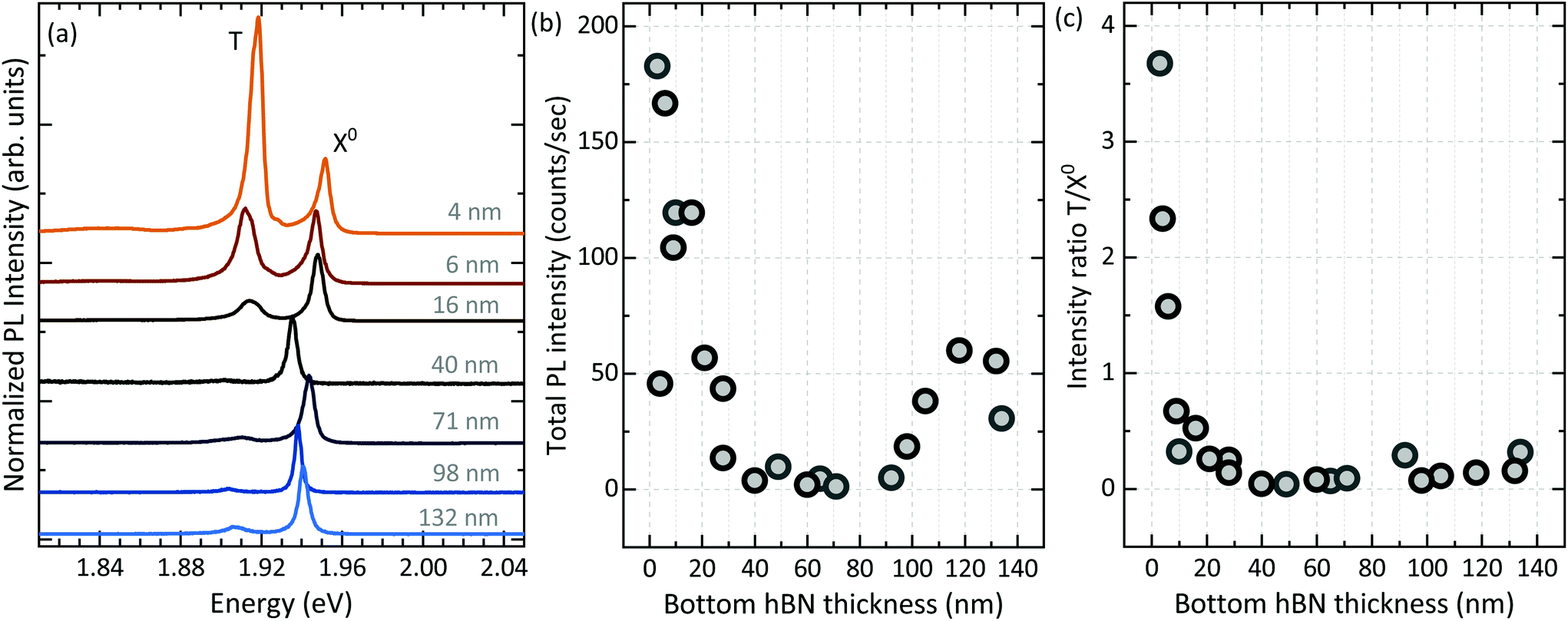 | ||
| Fig. 1 (a) Normalized PL spectra of hBN-encapsulated monolayer MoS2 measured at T = 5 K as a function of the bottom hBN flake thickness. The spectra are normalized to the maximum intensity of the neutral exciton emission (X0) for clarity. (b) Integrated intensity of the spectra shown in panel (a) and (c) the intensity ratio of the trion to the neutral exciton contributions (T/X0) vs. bottom hBN thickness. | ||
Now let us focus on the detailed analysis of the measured PL spectra. For the thinnest bottom hBN flake of 4 nm thickness, the T emission is much more intense as compared to the X0 one. When the bottom hBN flake gets thicker, the optical emission due to the neutral exciton starts to dominate the PL spectra, while the trion intensity substantially decreases. Fig. 1(c) demonstrates the intensity ratio of the T/X0 emissions as a function of the bottom hBN thickness. One can observe a decline in this ratio by two orders of magnitude from ∼3 to ∼0.03 with the hBN thickness approaching approx. 20 nm. For thicker hBN flakes the intensity ratio saturates at a roughly constant level. This behavior suggests the influence of external factors on the emission spectra and thus on the inherent properties of the studied MLs.
MoS2 crystals generally bear inherent n-type doping, including the MLs discussed within this report. This characteristic is linked to abundant sulfur vacancies in the bulk crystal.25–29 On the other hand, many reports show that the properties of this material vary depending on the structure in which it is used. In particular, encapsulating MoS2 significantly changes the optical or electrical performance of MLs, indicating their sensitivity to some external factors that affect their intrinsic properties.30–32
In our analysis, we adopt the reasoning that MLs obtained from a single bulk crystal share similar properties, particularly, a comparable level of doping. This means that the observed variation in the PL response within a given series of samples can be associated with the variation of the bottom hBN flake's thickness. The distinctly higher emission intensity of the T line compared to the X0 one for the thinnest bottom hBN flake is a signature of high electron concentration in these MoS2 MLs. We believe that the increased concentration stems from quantum tunneling of carriers from the impurities present in the SiO2/Si substrates.
As similar considerations have not been widely addressed in optical measurements, we invoke the results of electrical studies. Since hBN is an insulator with a large energy band gap, it is an excellent dielectric material that has been widely used as a building block of high-performance devices, i.a. as a tunneling barrier.33–37 Even though some reports suggest that a single atomic hBN layer acts as effective isolation,34 it is often found, that the very thin flakes do not provide efficient barriers for carriers.14,15 As the transmission probability of the hBN barrier decreases exponentially with the number of atomic layers, most devices rely on the barriers whose thicknesses fall in the single-nanometers range.36,38–41 However, the electron wave function can penetrate even larger number of layers, up to 9 nm thick.35,42–44
A parallel pattern can be found in our results, where the charge carrier tunneling seems to occur for structures with bottom hBN thickness below ∼10 nm, as manifested by the strong trion-related emission (see Fig. 1). Above this limit, the density of free carriers in the MoS2 MLs attains an inherent doping level of a natural crystal.
To provide an estimate of the carrier concentration in the investigated MLs, the extracted values of T/X0 ratio, presented in Fig. 1(c), are compared with the PL results measured as a function of free electron concentration in ref. 45. It has been found that the electron concentration (ne) equals about 3 × 1012 cm−2 in the MLs on 4 nm hBN, and then decreases by about one order of magnitude for ≥10 nm thick bottom hBN flake. The presented approach can be adapted to other S-TMDs MLs, such as MoSe2, MoTe2, WS2, and WSe2, which gives us a useful tool to tune the carrier concentration in S-TMD MLs deposited on hBN flakes.
2.2. Fine structure of negative trions
To investigate thoroughly the effect of the bottom hBN thickness on both the emission and absorption processes in MoS2 MLs, we have focused our further investigations based on three experimental techniques (PL, PLE, and RC) on selected samples with hBN substrate thicknesses of 6 nm, 16 nm, and 132 nm, see Fig. 2. As can be appreciated in the figure, the X0 and T resonances are apparent in all of the measured spectra. Let us turn the attention to a detailed analysis of the feature in the vicinity of the T complex. There are two well-resolved absorption-type resonances, which can be distinguished for the negative trions in the PLE and RC spectra. However, the corresponding PL spectra comprise up to three components. According to the recent works,21,46 a double structure of the negative trion in the MoS2 ML, apparent in the aforementioned PLE and RC signals, can be ascribed to the intravalley spin-singlet and intervalley spin-singlet negatively charged excitons for the higher and lower-energy features, respectively. Simultaneously, the assignement of the lowest energy resonance visible only in the PL spectra is more complicated. We have tentatively related it to the intervalley spin-triplet negatively charged exciton, which is described in details in the next Section. | ||
| Fig. 2 Selected low-temperature PL/PLE and RC spectra of hBN-encapsulated monolayer MoS2 with the thickness of the hBN substrate equal to 6 nm, 16 nm, 132 nm. | ||
It is also worth pointing out that the interference effects in the investigated dielectric stacks affect not only the overall PL intensity (see Fig. 1), but also the lineshape of resonances observed in the RC spectra (see Fig. 2). A similar effect on the observed RC features was reported for MoS2 MLs deposited on SiO2/Si substrates.47
The three-component fine structure of the negative trion, apparent in PL spectra, is displayed distinctly in Fig. 3(a), in which a combination of three Lorentzian curves was fitted to the data. The extracted energy separation between the T1 and T2 is equal to ∼7 meV, which is consistent with the corresponding value of around 8 meV resulting from our PLE and RC measurements, presented in Fig. 2, as well as the value reported in ref. 46. The extracted T2–T3 energy separation is of the order of 4 meV. The observation of the T3 line in the PL spectrum is most surprising as its contribution to the RC and PLE spectra is absent (see Fig. 2). To verify the origin of the T lines, the PL spectra have been measured with varying excitation power. The integrated intensities of the negative trions and the neutral exciton display a linear dependence on the excitation power, see Fig. 3(b), as is expected for excitonic features comprising a single electron–hole (e–h) pair.48
 | ||
| Fig. 3 (a) Photoluminescence spectrum of negative trions measured on the MoS2 monolayer with 10 nm-thick bottom hBN. The coloured Lorentzians display fits to the corresponding T1, T2, and T3 lines. (b) Integrated intensities of the negative trions and the neutral exciton as a function of excitation power. The dashed grey line is a guide to the eye indicating a linear increase. (c) Schematic illustration of possible spin configurations for optically-active (bright) negatively charged excitons formed in the K+ point in the monolayer MoS2. The T1, T2, and T3 states correspond to the intravalley spin singlet, the intervalley spin singlet, and the intervalley spin triplet. The figure illustrates complexes for which a hole is located at the K+ point of the Brillouin zone. | ||
The apparent fine structure of the negative trion might seem surprising, as the theoretically predicted structure of the conduction (CB) and valence (VB) bands leads to the optical activity of the energetically lowest transition.49 This picture however does not include the excitonic character of the optical response of S-TMD MLs.7 It has recently been demonstrated that the excitonic ground state in MoS2 MLs encapsulated in hBN is optically inactive or dark,50 which places this material within the family of so-called darkish MLs. For other darkish MLs, such as WS2 and WSe2, two configurations of the negative trions, i.e. the intravalley spin-singlet and intervalley spin-singlet states, were reported in the literature.51–54 It is important to mention that the small CB spin–orbit splitting in MoS2 MLs, predicted to be equal to about 3 meV,49 leads to yet another effect. This is the reordering of the spin-split and spin-polarized CB subbands in the K valley occupied by an electron–hole (e–h) pair forming a trion. The reordering results from a difference in the effective electron mass in the subbands combined with the e–h interaction (see ref. 21 and 46 for details). This leads to the same arrangement of CB subbands in both the K+ and K− points of the Brillouin zone, in contrast to the opposite arrangement in the W-based MLs.51–54 Consequently, three spin configurations of the optically-active (bright) negatively charged excitons in MoS2 MLs may be formed in the K+ valley, i.e. the intravalley spin singlet (T1), the intervalley spin singlet (T2), and the intervalley spin-triplet (T3), see ref. 55. Note that M. Drüppel et al.55 predicted theoretically three different configurations of negative trions taking into account that the excitonic ground state in MoS2 is bright (the reordering effect was not included), on the contrary to the demonstrated experimental dark ground state of exciton in ref. 50. Fig. 3(c) presents a schematic illustration of the discussed possible spin configurations for optically-active (bright) negative trions formed in the K+ point in the monolayer MoS2. Note that all corresponding negative trions can also be formed in the K− valley, which leads to two possible configurations of a given complex.
By comparing the measured RC, PLE, and PL spectra on the MoS2 MLs with 6 nm and 16 nm bottom hBN flakes (see Fig. 2) and the RC spectra reported in ref. 46, we relate the highest- (T1) and middle-energy (T2) resonances to the intravalley spin-singlet and intervalley spin-singlet negative trions, respectively. The assignment of the T3 is the most difficult, as its contribution is only manifested in the PL spectra and it has not been reported so far. We tentatively ascribe the T3 line to the emission of the intervalley spin-triplet state of the charged exciton, see Fig. 3(c). The intervalley trion is the energetically lowest, as the two electrons occupy both valleys allowing them to reside in the energetically lowest CB.55 The appearance of the T3 emission can be due to a photo-doping process in the PL experiment, which can explain the lack of the T3 contribution in the corresponding RC and PLE spectra. Recently, it has been demonstrated that the laser excitation may induce free electron concentration in MoS2 MLs ranging up to several times 1012 cm−2.56 Due to the small CB spin–orbit splitting and the photo-doping processes, we assumed that the Fermi level is high enough to provide free electrons on the higher energy CB subband allowing the formation of the intervalley triplet state of the negative trion.
In order to investigate the properties of the negative trions, the helicity-resolved PL spectra were measured on the MoS2 ML on the 6 nm bottom hBN flake in magnetic fields up to 10 T oriented perpendicularly to the ML's plane (out-of-plane configuration), see Fig. 4(a). Applying an out-of-plane magnetic field yields the excitonic Zeeman effect,57 which is apparent as splitting into two circularly polarized components of each transition. To facilitate the analysis of that evolution, we fitted these results with Lorentzian functions. The extracted transitions energies of both the σ+ and σ− polarized components as a function of magnetic fields are summarized in Fig. 4(b). As can be appreciated in the figure, all the σ+/σ− features experience a redshift/blueshift with increasing magnetic field. The energy evolution of the σ±-polarized lines, Eσ± can be described by the following equation:
 | (1) |
 | ||
| Fig. 4 (a) Helicity-resolved PL spectra of MoS2 monolayer with 6 nm-thick bottom hBN at selected values of the applied out-of-plane magnetic field. The red (blue) colour corresponds to the σ+ (σ−) polarized spectra. The spectra are vertically shifted for clarity. (b) Transition energies of the excitonic complexes extracted from the fits to the PL spectra as a function of magnetic field. The solid black curves represent fits with eqn (1). | ||
Apart from the aforementioned analysis of the magnetic-field dependence of transition energies, the applied magnetic field may also affect the emission intensities of the σ± components.54–57 As can be seen in Fig. 4(a), both σ± components of the X0 line are characterized by almost the same intensity in magnetic fields, which is characteristic for this complex in darkish MLs.7,46,57 Simultaneously, all trion-related emissions are polarized in higher fields. This effect is seen distinctly for the T1 and T2 line, for which the lower/higher energy (σ+/σ−) component gains in/loses intensity with the increased magnetic field. The observed evolution for the T1 and the T2 line is analogous to that observed in the RC spectra (see ESI†) and was previously reported in ref. 46. This effect can be understood in terms of thermal distribution of free electrons between the field-split states (see ref. 46 and 57 for details). In the case of the T3 line, the opposite behaviour is expected so that the magnetic field induces the gain/loss of higher/lower energy (σ−/σ+) component.55 Unfortunately, the quality of results, presented in Fig. 4(a), does not allow us to unquestionably assign it. Moreover, the understanding of the magnetic-field evolution of the T3 intensity can be more complicated, as the emission of this complex is observed due to the photo-doping effect. It should be also emphasized that the magnetic field dependence of trion intensities in ML MoS2 is completely different from the corresponding one observed for intravalley and intervalley negatively charged excitons in ML WS2.54
3. Conclusions
In summary, we have presented a systematic study of the effect of the bottom hBN thickness on the optical properties of hBN encapsulated MoS2 MLs. Our results demonstrate that high electron concentration in TMD MLs predominantly originates from charge transfer from the substrate. The hBN flakes used as substrates act as barriers for carriers provided by those impurities. The effectiveness of such a barrier depends on its thickness. This approach can be used to manipulate the carrier concentration in the studied material. The reported investigation has also allowed us to unravel the fine structure of the trion-related transition in the MoS2 MLs. The three optically active complexes have been attributed to the intravalley singlet, the intervalley singlet, and the intervalley triplet. The observation of the latter transition in the emission is related to the small CB spin–orbit splitting in ML MoS2 and the photo-doping processes. The effective g-factors of all trion complexes have been determined. The existence of these trion features confirms the reordering of the spin-split and spin-polarized CB subbands in the K valley, allowing the three spin configurations of the bright negatively charged excitons. Given that substrates are typically needed for most research and applications, our results are highly relevant allowing for a deeper qualitative understanding of environmentally induced changes on intrinsic properties of S-TMDs MLs.Author contributions
M. G. and K. O-P. fabricated samples, K. W. and T. T. provided the hBN crystal, P. K. provided experimental equipment, M. G. and M. R. M. carried out the experiments and performed the data analysis. K. O-P. and K. N. did the AFM characterization of the samples. M. G., A. B., and M. R. M. prepared the manuscript with contribution from all other co-authors.Conflicts of interest
There are no conflicts to declare.Acknowledgements
The work has been supported by the National Science Centre, Poland (grant no. 2017/27/B/ST3/00205, 2017/27/N/ST3/01612, 2018/31/B/ST3/02111), EU Graphene Flagship project (no. 785219), the ATOMOPTO project (TEAM programme of the Foundation for Polish Science, co-financed by the EU within the ERD-Fund), and the CNRS via IRP “2DM” project. K. W. and T. T. acknowledge support from the Elemental Strategy Initiative conducted by the MEXT, Japan, (grant no. JPMXP0112101001), JSPS KAKENHI (grant no. JP20H00354), and the CREST (JPMJCR15F3), JST.References
- M.-Y. Li, C.-H. Chen, Y. Shi and L.-J. Li, Mater. Today, 2016, 19(6), 322–335, DOI:10.1016/j.mattod.2015.11.003.
- A. K. Geim and I. V. Grigorieva, Nature, 2013, 499, 419–425, DOI:10.1038/nature12385.
- Y. Guo, X. Wei, J. Shu, B. Liu, J. Yin, C. Guan, Y. Han, S. Gao and Q. Chen, Appl. Phys. Lett., 2015, 106, 103109, DOI:10.1063/1.4914968.
- Y. Kang and S. Han, Nanoscale, 2017, 9, 4265–4271, 10.1039/C6NR08555E.
- S. Borghardt, J.-S. Tu, F. Winkler, J. Schubert, W. Zander, K. Leosson and B. E. Kardynał, Phys. Rev. Mater., 2017, 1(5), 054001, DOI:10.1103/PhysRevMaterials.1.054001.
- S. Ghatak, A. N. Pal and A. Ghosh, ACS Nano, 2011, 5(10), 7707–7712, DOI:10.1021/nn202852j.
- M. R. Molas, A. O. Slobodeniuk, K. Nogajewski, M. Bartos, L. Bala, A. Babiński, K. Watanabe, T. Taniguchi, C. Faugeras and M. Potemski, Phys. Rev. Lett., 2019, 123(13), 136801, DOI:10.1103/PhysRevLett.123.136801.
- D. Sercombe, S. Schwarz, O. D. Pozo-Zamudio, F. Liu, B. J. Robinson, E. A. Chekhovich, I. I. Tartakovskii, O. Kolosov and A. I. Tartakovskii, Sci. Rep., 2013, 3, 3489, DOI:10.1038/srep03489.
- Q. H. Wang, Z. Jin, K. K. Kim, A. J. Hilmer, G. L. C. Paulus, C.-J. Shih, M.-H. Ham, J. D. Sanchez-Yamagishi, K. Watanabe, T. Taniguchi, J. Kong, P. Jarillo-Herrero and M. S. Strano, Nat. Chem., 2012, 4, 724–732, DOI:10.1038/nchem.1421.
- M. Grzeszczyk, M. R. Molas, M. Bartoš, K. Nogajewski, M. Potemski and A. Babiński, Appl. Phys. Lett., 2020, 116, 191601, DOI:10.1063/1.5128048.
- F. Withers, O. D. Pozo-Zamudio, A. Mishchenko, A. P. Rooney, A. Gholinia, K. Watanabe, T. Taniguchi, S. J. Haigh, A. K. Geim, A. I. Tartakovskii and K. S. Novoselov, Nat. Mater., 2015, 14, 301–306, DOI:10.1038/nmat4205.
- J. Binder, F. Withers, M. R. Molas, C. Faugeras, K. Nogajewski, K. Watanabe, T. Taniguchi, A. Kozikov, A. K. Geim, K. S. Novoselov and M. Potemski, Nano Lett., 2017, 17, 1425–1430, DOI:10.1021/acs.nanolett.6b04374.
- K. Novoselov, O. A. Mishchenko, O. A. Carvalho and A. C. Neto, Science, 2016, 353(6298), aac9439, DOI:10.1126/science.aac9439.
- Y. Y. Illarionov, G. Rzepa, M. Waltl, T. Knobloch, A. Grill, M. M. Furchi, T. Mueller and T. Grasser, 2D Mater., 2016, 3, 035004, DOI:10.1088/2053-1583/3/3/035004.
- K. Dolui, I. Rungger and S. Sanvito, Phys. Rev. B: Condens. Matter Mater. Phys., 2013, 87, 165402, DOI:10.1103/PhysRevB.87.165402.
- M. Buscema, G. A. Steele, H. S. J. van der Zant and A. Castellanos-Gomez, Nano Res., 2014, 7, 561–571, DOI:10.1007/s12274-014-0424-0.
- B. Yang, E. Molina, J. Kim, D. Barroso, M. Lohmann, Y. Liu, Y. Xu, R. Wu, L. Bartels, K. Watanabe, T. Taniguchi and J. Shi, Nano Lett., 2018, 18, 3580–3585, DOI:10.1021/acs.nanolett.8b00691.
- F. Cadiz, E. Courtade, C. Robert, G. Wang, Y. Shen, H. Cai, T. Taniguchi, K. Watanabe, H. Carrere, D. Lagarde, M. Manca, T. Amand, P. Renucci, S. Tongay, X. Marie and B. Urbaszek, Phys. Rev. X, 2017, 7(2), 021026, DOI:10.1103/PhysRevX.7.021026.
- T. Jakubczyk, G. Nayak, L. Scarpelli, W.-L. Liu, S. Dubey, N. Bendiab, L. Marty, T. Taniguchi, K. Watanabe, F. Masia, G. Nogues, J. Coraux, W. Langbein, J. Renard, V. Bouchiat and J. Kasprzak, ACS Nano, 2019, 13(3), 3500–3511, DOI:10.1021/acsnano.8b09732.
- C. Robert, M. A. Semina, F. Cadiz, M. Manca, E. Courtade, T. Taniguchi, K. Watanabe, H. Cai, S. Tongay, B. Lassagne, P. Renucci, T. Amand, X. Marie, M. M. Glazov and B. Urbaszek, Phys. Rev. Mater., 2018, 2(1), 011001, DOI:10.1103/PhysRevMaterials.2.011001.
- J. Jadczak, J. Kutrowska-Girzycka, M. Bieniek, T. Kazimierczuk, P. Kossacki, J. Schindler, J. Debus, K. Watanabe, T. Taniguchi and C.-H. Ho, et al. , Nanotechnology, 2021, 32, 145717, DOI:10.1088/1361-6528/abd507.
- H. Zhang, Y. Wan, Y. Ma, W. Wang, Y. Wang and L. Dai, Appl. Phys. Lett., 2015, 107, 101904, DOI:10.1063/1.4961671.
- A. Castellanos-Gomez, R. Roldán, E. Cappelluti, M. Buscema, F. Guinea, H. S. van der Zant and G. A. Steele, Nano Lett., 2013, 13(11), 5361–5366, DOI:10.1021/nl402875m.
- R. Yan, S. Bertolazzi, J. Brivio, T. Fang, A. Konar, A. G. Birdwell, N. Nguyen, A. Kis, D. Jena and H. G. Xing, 2012, arXiv preprint arXiv:1211.4136.
- Z. Lin, B. R. Carvalho, E. Kahn, R. Lv, R. Rao, H. Terrones, M. A. Pimenta and M. Terrones, 2D Mater., 2016, 3, 022002, DOI:10.1088/2053-1583/3/2/022002.
- A. K. Saha and M. Yoshiya, Phys. B, 2018, 532(1), 184–194, DOI:10.1016/j.physb.2017.07.026.
- J. Hong, Z. Hu, M. Probert, K. Li, D. Lv, X. Yang, L. Gu, N. Mao, Q. Feng and L. Xie, et al. , Nat. Commun., 2015, 6, 1–8, DOI:10.1038/s41467-017-02172-1.
- Z. Yu, Y. Pan, Y. Shen, Z. Wang, Z.-Y. Ong, T. Xu, R. Xin, L. Pan, B. Wang and L. Sun, et al. , Nat. Commun., 2014, 5, 1–7, DOI:10.1038/ncomms6290.
- D. Liu, Y. Guo, L. Fang and J. Robertson, Appl. Phys. Lett., 2013, 103, 183113, DOI:10.1063/1.4824893.
- B. W. Baugher, H. O. Churchill, Y. Yang and P. Jarillo-Herrero, Nano Lett., 2013, 13, 4212–4216, DOI:10.1021/nl401916s.
- H. Wang, L. Yu, Y.-H. Lee, Y. Shi, A. Hsu, M. L. Chin, L.-J. Li, M. Dubey, J. Kong and T. Palacios, Nano Lett., 2012, 12, 4674–4680, DOI:10.1021/nl302015v.
- B. Radisavljevic and A. Kis, Nat. Mater., 2013, 12, 815–820, DOI:10.1038/nmat3687.
- A. Young, C. Dean, I. Meric, S. Sorgenfrei, H. Ren, K. Watanabe, T. Taniguchi, J. Hone, K. Shepard and P. Kim, Phys. Rev. B: Condens. Matter Mater. Phys., 2012, 85(23), 235458, DOI:10.1103/PhysRevB.85.235458.
- L. Britnell, R. V. Gorbachev, R. Jalil, B. D. Belle, F. Schedin, M. I. Katsnelson, L. Eaves, S. V. Morozov, A. S. Mayorov and N. M. Peres, et al. , Nano Lett., 2012, 12(3), 1707–1710, DOI:10.1021/nl3002205.
- L. Britnell, R. Gorbachev, R. Jalil, B. Belle, F. Schedin, A. Mishchenko, T. Georgiou, M. Katsnelson, L. Eaves and S. Morozov, et al. , Science, 2012, 335(6071), 947–950, DOI:10.1126/science.1218461.
- M. Z. Iqbal, S. Siddique, M. F. Khan, A. U. Rehman, A. Rehman and J. Eom, Adv. Eng. Mater., 2018, 20, 1800159 CrossRef.
- A. Mishchenko, J. Tu, Y. Cao, R. V. Gorbachev, J. Wallbank, M. Greenaway, V. Morozov, S. Morozov, M. Zhu and S. Wong, et al. , Nat. Nanotechnol., 2014, 9, 808–813, DOI:10.1038/nnano.2014.187.
- S. Jung, N. Myoung, J. Park, T. Y. Jeong, H. Kim, K. Watanabe, T. Taniguchi, D. H. Ha, C. Hwang and H. C. Park, Nano Lett., 2017, 17(1), 206–213, DOI:10.1021/acs.nanolett.6b03821.
- C. R. Paul Inbaraj, R. J. Mathew, R. K. Ulaganathan, R. Sankar, M. Kataria, H. Y. Lin, H.-Y. Cheng, K.-H. Lin, H.-I. Lin and Y.-M. Liao, et al. , ACS Appl. Mater. Interfaces, 2020, 12(23), 26213–26221, DOI:10.1021/acsami.0c06077.
- M. Z. Iqbal and M. M. Faisal, J. Appl. Phys., 2019, 125, 084902 CrossRef.
- D. Chu, Y. H. Lee and E. K. Kim, Sci. Adv., 2017, 3(4), e1602726, DOI:10.1126/sciadv.1602726.
- S. Kang, N. Prasad, H. C. Movva, A. Rai, K. Kim, X. Mou, T. Taniguchi, K. Watanabe, L. F. Register and E. Tutuc, et al. , Nano Lett., 2016, 16, 4975–4981, DOI:10.3390/cryst8020070.
- G.-H. Lee, Y.-J. Yu, C. Lee, C. Dean, K. L. Shepard, P. Kim and J. Hone, Appl. Phys. Lett., 2011, 99, 243114, DOI:10.1063/1.3662043.
- K. Kim, N. Prasad, H. C. Movva, G. W. Burg, Y. Wang, S. Larentis, T. Taniguchi, K. Watanabe, L. F. Register and E. Tutuc, Nano Lett., 2018, 18, 5967–5973, DOI:10.1021/acsnano.0c08133.
- J. Klein, A. Hötger, M. Florian, A. Steinhoff, A. Delhomme, T. Taniguchi, K. Watanabe, F. Jahnke, A. W. Holleitner, M. Potemski, et al., 2020, arXiv preprint arXiv:2007.14441.
- J. G. Roch, G. Froehlicher, N. Leisgang, P. Makk, K. Watanabe, T. Taniguchi and R. J. Warburton, Nat. Nanotechnol., 2019, 14, 432–436, DOI:10.1038/s41565-019-0397-y.
- X. Li, Y. Shi, S. Li, W. Shi, W. Han, C. Zhou, X. Zhao and B. Liang, Opt. Mater. Express, 2018, 8, 3082, DOI:10.1364/OME.8.003082.
- C. F. Klingshirn, Semiconductor Optics, Springer Berlin Heidelberg, 2012 Search PubMed.
- A. Kormányos, G. Burkard, M. Gmitra, J. Fabian, V. Zólyomi, N. D. Drummond and V. Fal’ko, 2D Mater., 2015, 2, 022001, DOI:10.1088/2053-1583/2/2/022001.
- C. Robert, B. Han, P. Kapuscinski, A. Delhomme, C. Faugeras, T. Amand, M. R. Molas, M. Bartos, K. Watanabe, T. Taniguchi, B. Urbaszek, M. Potemski and X. Marie, Nat. Commun., 2020, 11, 4037, DOI:10.1038/s41467-020-17608-4.
- E. Courtade, M. Semina, M. Manca, M. M. Glazov, C. Robert, F. Cadiz, G. Wang, T. Taniguchi, K. Watanabe, M. Pierre, W. Escoffier, E. L. Ivchenko, P. Renucci, X. Marie, T. Amand and B. Urbaszek, Phys. Rev. B: Condens. Matter Mater. Phys., 2017, 96(8), 085302, DOI:10.1103/PhysRevB.96.085302.
- D. Vaclavkova, J. Wyzula, K. Nogajewski, M. Bartos, A. O. Slobodeniuk, C. Faugeras, M. Potemski and M. R. Molas, Nanotechnology, 2018, 29, 325705, DOI:10.1088/1361-6528/aac65c.
- T. P. Lyons, S. Dufferwiel, M. Brooks, F. Withers, T. Taniguchi, K. Watanabe, K. S. Novoselov, G. Burkard and A. I. Tartakovskii, Nat. Commun., 2019, 10, 2330, DOI:10.1038/s41467-019-10228-7.
- P. Kapuściński, D. Vaclavkova, M. Grzeszczyk, A. O. Slobodeniuk, K. Nogajewski, M. Bartos, K. Watanabe, T. Taniguchi, C. Faugeras, A. Babiński, M. Potemski and M. R. Molas, Phys. Chem. Chem. Phys., 2020, 22, 19155–19161, 10.1039/D0CP02737E.
- M. Drüppel, T. Deilmann, P. Krüger and M. Rohlfing, Nat. Commun., 2017, 8, 1–7, DOI:10.1038/s41467-017-02286-6.
- A. C. Gadelha, A. R. Cadore, L. Lafeta, A. M. de Paula, L. M. Malard, R. G. Lacerda and L. C. Campos, Nanotechnology, 2020, 31, 255701, DOI:10.1088/1361-6528/ab7de2.
- M. Koperski, M. R. Molas, A. Arora, K. Nogajewski, M. Bartos, J. Wyzula, D. Vaclavkova, P. Kossacki and M. Potemski, 2D Mater., 2018, 6, 015001, DOI:10.1088/2053-1583/aae14b.
- M. Goryca, J. Li, A. V. Stier, T. Taniguchi, K. Watanabe, E. Courtade, S. Shree, C. Robert, B. Urbaszek and X. Marie, et al. , Nat. Commun., 2019, 10, 1–12, DOI:10.1038/s41467-019-12180-y.
Footnote |
| † Electronic supplementary information (ESI) available: Sample fabrication, experimental details and reflectance contrast results in magnetic field. See DOI: 10.1039/d1nr03855a |
| This journal is © The Royal Society of Chemistry 2021 |