
 Open Access Article
 This Open Access Article is licensed under a
 Creative Commons Attribution 3.0 Unported Licence
Superconducting boron doped nanocrystalline diamond on boron nitride ceramics
Soumen
Mandal
 *a,
Henry A.
Bland
a,
Jerome A.
Cuenca
a,
Malcolm
Snowball
b and
Oliver A.
Williams
*a
*a,
Henry A.
Bland
a,
Jerome A.
Cuenca
a,
Malcolm
Snowball
b and
Oliver A.
Williams
*a
aSchool of Physics and Astronomy, Cardiff University, Cardiff, UK. E-mail: mandals2@cardiff.ac.uk; soumen.mandal@gmail.com; williamso@cardiff.ac.uk
bUltra Biotecs Limited, Derby, UK
First published on 8th May 2019
Abstract
In this work we have demonstrated the growth of nanocrystalline diamond on boron nitride ceramic. We measured the zeta potential of the ceramics to select the diamond seeds. Diamond was then grown on the seeded ceramics using a microwave chemical vapour deposition system. A clear difference was found between the samples which were seeded with nanodiamond and the ones not seeded before growth. Raman spectroscopy confirmed the excellent quality of the diamond film. Dielectric measurements showed an increase in the dielectric constant of the material after diamond growth. The diamond was also doped with boron to make it superconducting. The film had a transition temperature close to 3.4 K. Similar strategies can be applied for the growth of diamond on other types of ceramics.
1. Introduction
Boron and nitrogen belonging to group III and V in the periodic table can combine in a 1![[thin space (1/6-em)]](https://www.rsc.org/images/entities/char_2009.gif) :1 ratio to form boron nitride (BN). Primarily it has three different forms: (1) α-BN: also known as hexagonal boron nitride (h-BN) or “white graphite” with a structure closely matching that of graphite, (2) β-BN: also known as cubic boron nitride (c-BN) and has a structure analogous to diamond, and (3) γ-BN: which has a wurtzite (w-BN) structure.1 Other forms like turbostratic (t-BN),2 rhombohedral (r-BN)3,4 and amorphous5–7 (a-BN) boron nitride are also seen. In this work we will be using ceramics derived from h-BN only. Historically, boron nitride was first synthesised by Balmain in 18428 and h-BN was hot pressed into machinable ceramics for the first time in 1952.9
:1 ratio to form boron nitride (BN). Primarily it has three different forms: (1) α-BN: also known as hexagonal boron nitride (h-BN) or “white graphite” with a structure closely matching that of graphite, (2) β-BN: also known as cubic boron nitride (c-BN) and has a structure analogous to diamond, and (3) γ-BN: which has a wurtzite (w-BN) structure.1 Other forms like turbostratic (t-BN),2 rhombohedral (r-BN)3,4 and amorphous5–7 (a-BN) boron nitride are also seen. In this work we will be using ceramics derived from h-BN only. Historically, boron nitride was first synthesised by Balmain in 18428 and h-BN was hot pressed into machinable ceramics for the first time in 1952.9
Due to its combination of unique properties like high thermal conductivity, high oxidation resistance, chemical inertness and high dielectric constant it is an excellent candidate for a variety of applications.10–13 In particular, the dielectric properties and high thermal conductivity of boron nitride find usage in electronic and electrical applications.11,14,15 Further enhancement of dielectric properties in BN ceramics can be achieved by applying a thin coat of a high dielectric material like diamond (dielectric constant 5.6 (ref. 16)). Since diamond is not machinable and forming large work pieces wholly from diamond is extremely expensive it is suitable to coat a thin layer of diamond on machinable ceramics to enhance the properties of ceramics. With the advancement of growth technology it is possible to grow diamond on a variety of substrates.17 However, the large difference between the surface energies18,19 of diamond and BN makes it impossible to heteroepitaxially grow diamond on BN. Hence, a seeding step is needed to grow diamond on BN ceramics. In the literature, a variety of seeding techniques can be found.17 For this study we have used an electrostatic nanodiamond colloid based seeding technique. The nanodiamond seeds in the colloid can be both positively or negatively charged depending on the surface termination.20 So for the seeding of the BN substrate it is essential to know the surface charge or zeta (ζ) potential of BN ceramics. In this work we have determined the ζ-potential of the ceramic, which was used to select the diamond seed solution. Diamond thin films were grown on the ceramic using microwave plasma chemical vapour deposition and the dielectric constant of the diamond-BN ceramic was measured. Furthermore, to test the properties of the diamond film, the layer was doped with boron to test its superconducting properties. The growth of diamond on ceramics can be used to enhance the dielectric properties of ceramic electrical components. BN ceramic can also be used to form a custom porous network to grow doped diamond. After the growth the BN ceramic can be removed with a suitable chemical process and the free standing network can be filled with a suitable electrolyte to form supercapacitors as has been described by Yu et al.21 using a silicon carbide template. The advantage of BN ceramic is its machinability into regular and irregular shapes. Raman studies on doped and undoped diamond layers were done to determine the quality of the layer and scanning electron microscopy was used to observe the crystalline quality and diamond-BN interface of the layer.
2. Experimental
The diamond growth was done on commercially available parallel pressed boron nitride ceramics. The binder for the ceramic was boric oxide. The ceramic was shaped into a 10 by 10 mm square. The thickness of the squares was 0.5 mm. The dielectric constant of the supplied material at 1 MHz was 4.2 in the perpendicular direction as mentioned in the supplier's data sheet. The ζ-potential of BN ceramics was measured using a Surpass™ 3 electrokinetic analyser. The analyser measures the streaming potential by measuring the change in potential or current between two Ag/AgCl electrodes at the ends of a streaming channel as an electrolyte is passed through. Counter-ions from the charged surfaces are sheared by the flowing electrolyte creating a streaming current across the electrodes. The flow of counter-ions is dependent on the electric double layer of the surfaces. Hence, a measure of the streaming current is related to the ζ-potential of the surface.22 The setup for measuring the zeta potential of flat surfaces was suggested by Van-Wagnen et al.22 and has been used successfully to determine the ζ-potential of a variety of flat surfaces.23–26 A 10–3 M solution of potassium chloride was used as the electrolyte and the pressure was changed between 600 and 200 mbar. The channel width, formed between the BN plates, was kept constant at 100 μm. The pH of the electrolyte was varied by adding 0.1 M HCl and 0.1 M NaOH solutions with an inbuilt titrator in Surpass™ 3.The diamond films were grown in a Seki Technotron AX6500 series microwave chemical vapour deposition (CVD) system. A gas mixture of methane, hydrogen and trimethylboron (TMB) was used during the growth of doped diamond. The methane concentration in the mixture was 3%. The TMB was sourced from a premixed hydrogen/TMB gas mixture with 2000 ppm TMB concentration. Extra hydrogen was added to the reactor to get the desired methane concentration. The B/C ratio in the gas mixture during growth was calculated to be 12800 ppm. For growing undoped diamond only hydrogen and methane were used. The microwave power and gas pressure during growth were 4 kW and 50 Torr respectively. The temperature of the film during growth, as measured by using a Wiliamson dual wavelength pyrometer, was ∼800 °C. Before film growth, the substrates were briefly immersed in a mono-disperse aqueous colloid of hydrogen terminated diamond nanoparticles. Full details for the preparation of the diamond seed solution can be found elsewhere.20 In this case the BN plates were only immersed in the diamond solution not agitated like earlier experiments.27–29 This is due to the fact that on agitation the BN ceramics started dissociating in the seed solution. After seeding the substrates were rinsed thoroughly in DI water and blow dried. The dried substrates were then prebaked on a hot plate at 120 °C for 12 hours prior to growth. This step was done to expel easily absorbed moisture from the ceramic substrates. The baked substrates were then directly transferred from the hotplate to the reactor to minimise moisture absorption from the atmosphere. In Fig. 1 we have shown the image of a bare substrate in Panel A. Panel B shows a seeded substrate, without prebaking, after being exposed to initial plasma conditions. We can clearly see exposed white areas, which are formed due to the blister like formation and subsequent peel-off during the initial plasma stage of the growth. The initial plasma condition is when the microwave generator is turned on at low pressures to create the plasma. In our case that is 1.5 kW microwave power and 5 Torr gas pressure. Considering the fact that sample heating in the CVD reactor is due to the plasma, it can be said that the initial plasma conditions will not lead to extremely high temperatures in the substrate. The blistering under low power density conditions may be due to absorbed water in the substrates. The absorbed water interacts with the microwave and is immediately converted to vapour leading to blister formation. To test the hypothesis, we baked a seeded substrate at 120 °C for 12 hours on a hotplate and the sample was grown as explained previously. The image of a blister free diamond layer grown by this method is shown in Fig. 1C. From the above, it seems that blister formation is mainly due to absorbed water in the ceramics. The problem can be rectified in two possible ways (i) replace the hygroscopic boron oxide binder with a non-hygroscopic binder, (ii) the use of a hot filament CVD reactor instead of microwave CVD. As explained above, the microwave starts reacting with the absorbed water even before the sample heats up (lowest microwave power). In a hot filament reactor the conversion of absorbed water to vapour will be only through heating of the sample and we have shown sample heating prior to growth helps in reducing the blisters.
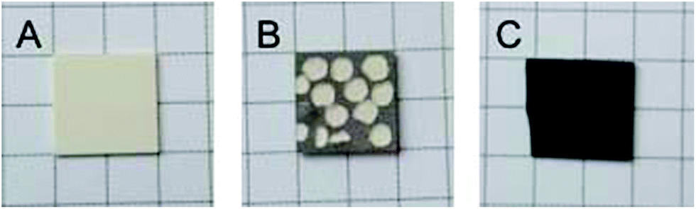 | ||
| Fig. 1 Image showing the as-received BN ceramic (Panel A). Panel B shows the sample exposed to initial plasma conditions after seeding with nanodiamond but without prebaking. Clear white areas can be seen where the blisters had formed and removed the top surface of the ceramic. Panel C shows a blister free diamond layer on BN ceramics. The sample was seeded with nanodiamond and prebaked before growth. | ||
Scanning electron microscopy (SEM) images were taken using a Hitachi SU8200 series FESEM operating at 20 kV and working distances between 9 and 11 mm. Raman measurements were done using an inVia Renishaw confocal microscope using a 514 nm laser. The excitation wavelength of 514 nm was used as it allows the excitation of both sp2 and sp3 carbon sites in the diamond film.30 The dielectric constant and loss of the samples were measured using a Keysight dielectric test fixture and impedance analyser (16451B and E4099A) in the range of 1 kHz to 1 MHz. More details about the measurement will be published elsewhere.31 The superconductivity in the films was measured using a Quantum Design Physical Properties Measurement System. The sample was measured in the temperature range of 2–300 K using four silver pasted contacts in the van der Pauw configuration. An excitation current of 5 μA was used for the measurement.
3. Results and discussion
3.1. Zeta potential
Fig. 2 shows the ζ-potential of the BN ceramic as a function of pH in the range of 3–9. The ζ-potential is negative in the measurement range. On extending the data, we estimate that the isoelectric point (IEP) for the material will be at pH ∼2.6. Since, the diamond solution used for seeding is in water, the region of interest is in the pH range 6–7. Considering the negative ζ-potential in this range a hydrogen terminated diamond seed solution, which shows a positive ζ-potential,32 is ideal for seeding the ceramic for diamond growth. A similar negative potential has also been seen for BN solutions.33,34 In the literature, a higher negative ζ-potential in boron ceramics has been attributed to a low content of B2O3.33,35 The IEP of the ceramic between pH 2–3, points to a strongly acidic solid similar to silica.36 This is surprising since boric acid, used as a binder for the ceramic, is a weak acid.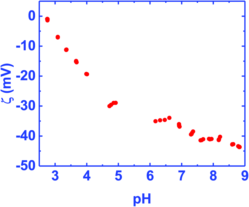 | ||
| Fig. 2 Zeta potential of BN ceramics in the pH range 3–9. The zeta potential is mostly negative in the range of measurement. On extending the data the iso-electric point is close to pH 2.6. | ||
3.2. Scanning electron microscopy
Fig. 3 shows the SEM images of diamond grown on BN ceramics. As evident from Fig. 2, we have to use positively charged diamond particles for seeding. The seeding was done using a nanodiamond solution containing 5 nm hydrogen terminated nanodiamond particles. To check the effectiveness of the seeding process we have grown diamond on both seeded and unseeded substrates in the same growth run. Fig. 3A shows the diamond grown on a seeded BN composite while panel C in the same figure shows the growth on an unseeded substrate. The seeded substrate shows a pinhole free diamond film. A magnified view of the diamond film is shown in Fig. 3B. The growth of diamond on the unseeded BN composite, shown in Fig. 3C, is sparse and we see individual grains on the surface. A magnified view of the individual diamond grains show good quality diamond grains (Fig. 3D). Also, we have tried growing diamond on composites brushed with 5 nm diamond seeds. This was done to verify if nanodiamond seed solutions are necessary for diamond growth, since, the process of making the nanodiamond seed solution is not trivial. The SEM images of such films are shown in Fig. 4. In panel A of Fig. 4 we have shown the overview of the diamond with pinhole free growth. A magnified view of the film with good quality crystal is shown in Fig. 4B. Even though at the microscopic scale there is not much difference between films grown by colloid or brushing the nanodiamond on the composite, using the colloid enabled the growth of blister free samples. The growth of blister free diamond samples was not possible even after post baking on substrates that were brushed with nanodiamond seeds (see Fig. 1B). Lastly, we have grown a sample with brushing of nanodiamond seeds after wetting the substrate in DI water for 10 minutes. In this case as well blister free samples could be grown. This means wetting and postbaking are important for blister free growth using microwave CVD. Also, it is to be noted that the use of the nanodiamond seed solution is not necessary for the growth of diamond on BN ceramics, brushing with nanodiamond powder along with wetting and postbaking is sufficient. Alternative seeding techniques like polymer coating assisted seeding37 or chemical nucleation38 may also be helpful in diamond growth on BN ceramics.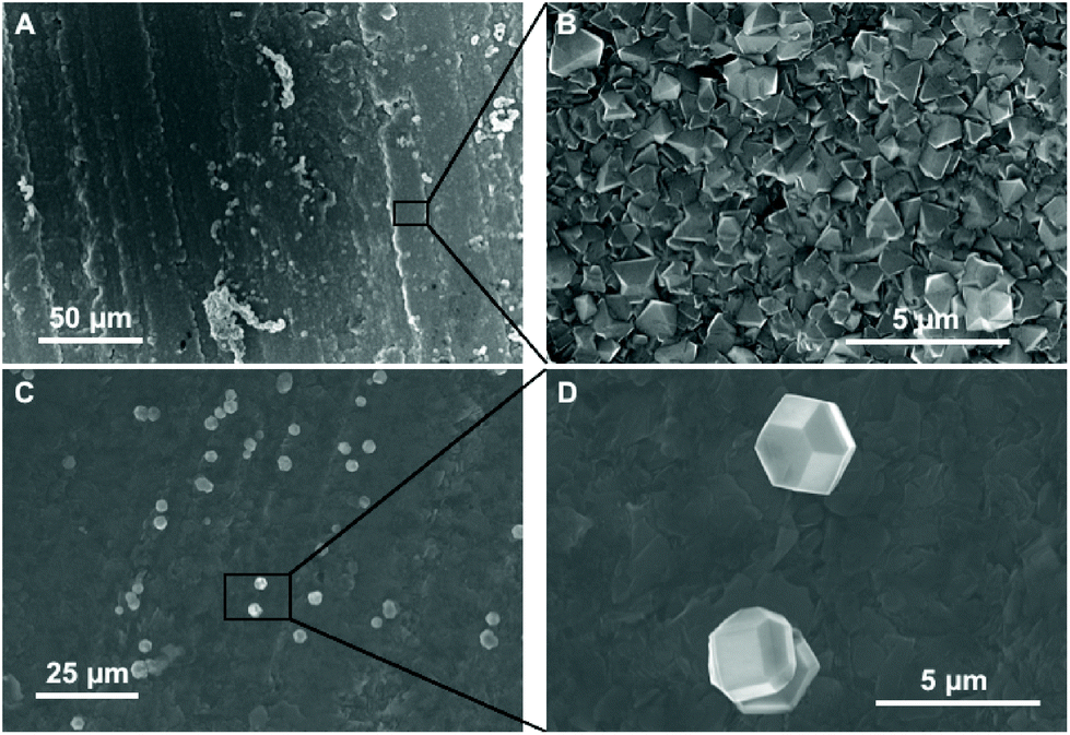 | ||
| Fig. 3 SEM images of diamond grown on BN ceramics. Panel A shows a pinhole free diamond film grown on the ceramic seeded with nanodiamond seeds. Panel B is a magnified image of the diamond film shown in panel A. Diamond crystals of varying sizes can be seen which is a characteristic of nanocrystalline diamond films. Panel C shows the growth of individual seeds on the composite. The composite was unseeded to study the effectiveness of seeding. Panel D shows the magnified image of two microcrystals grown on the unseeded BN composite. | ||
 | ||
| Fig. 4 SEM images of diamond grown on BN ceramics which were seeded by brushing dry nanodiamond powder. Panel A shows a pinhole free diamond layer. Panel B shows a magnified image of the diamond layer showing nanodiamond crystals. | ||
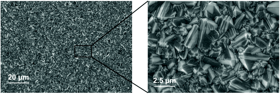
Finally, we have imaged the cross-section of the diamond-BN composite. Fig. 5 shows the cross-section of the diamond-BN interface. In panel A we have shown the overview of the film grown on BN. Panel B and C show the subsequent magnified image of the interface as specified in the figure by the black squares. In panel B we can clearly see the dense diamond layer on top. The BN composite with elongated nitride crystals can be seen at the bottom. The diamond layer is approximately 5 micron thick in this case. The magnified image of the interface in panel C shows a continuous diamond layer without large scale voids.
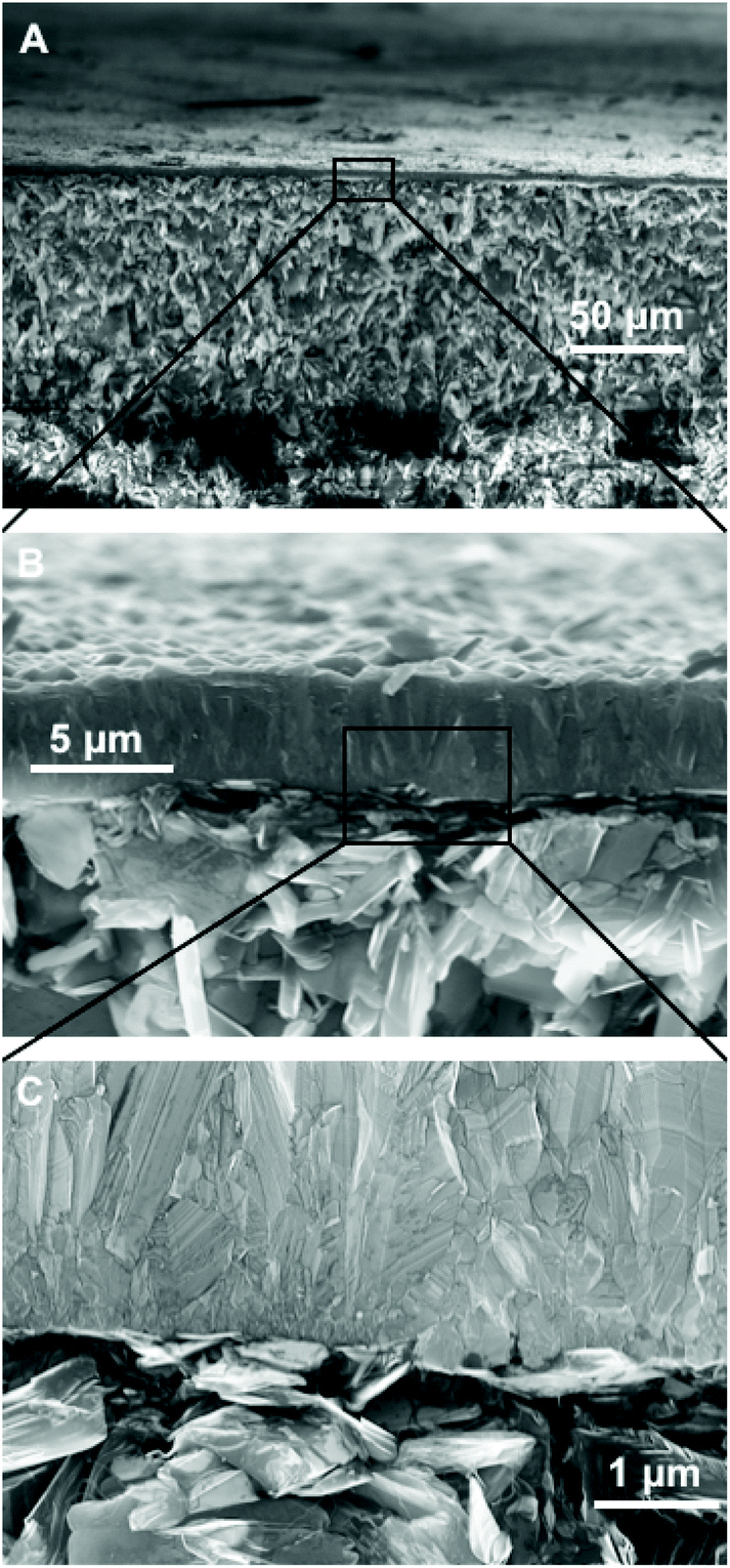 | ||
| Fig. 5 SEM image of the cross-section of diamond grown on BN ceramics. Panel A shows an overview of the diamond grown on BN ceramics. We can see the thin diamond layer on the top. Panel B and Panel C are successive magnified images of the interface. | ||
3.3. Raman spectroscopy
In this work we have grown both doped and undoped diamond on BN ceramics. Fig. 6 shows the Raman spectra of the bare substrate (black), intrinsic nanocrystalline diamond (red) and boron doped nanocrystalline diamond (green) grown on BN substrates. The dotted lines show the position of standard peaks. The h-BN and c-BN peaks should appear at 1364 and 1055 cm−1 respectively.39 The bare substrate shows a sharp h-BN peak and no c-BN peak indicating the presence of only h-BN in the composite. The spectra of undoped diamond grown on the composite is shown in red. We see a clear diamond peak40–42 at 1332 cm−1 along with a smaller h-BN peak. The diamond layer does not show any non-diamond carbon in the layer. Finally we have done Raman spectroscopy on the boron doped diamond (BDD) layer grown on the composite. The spectrum is similar to those of BDD layers grown on silicon substrates.43,44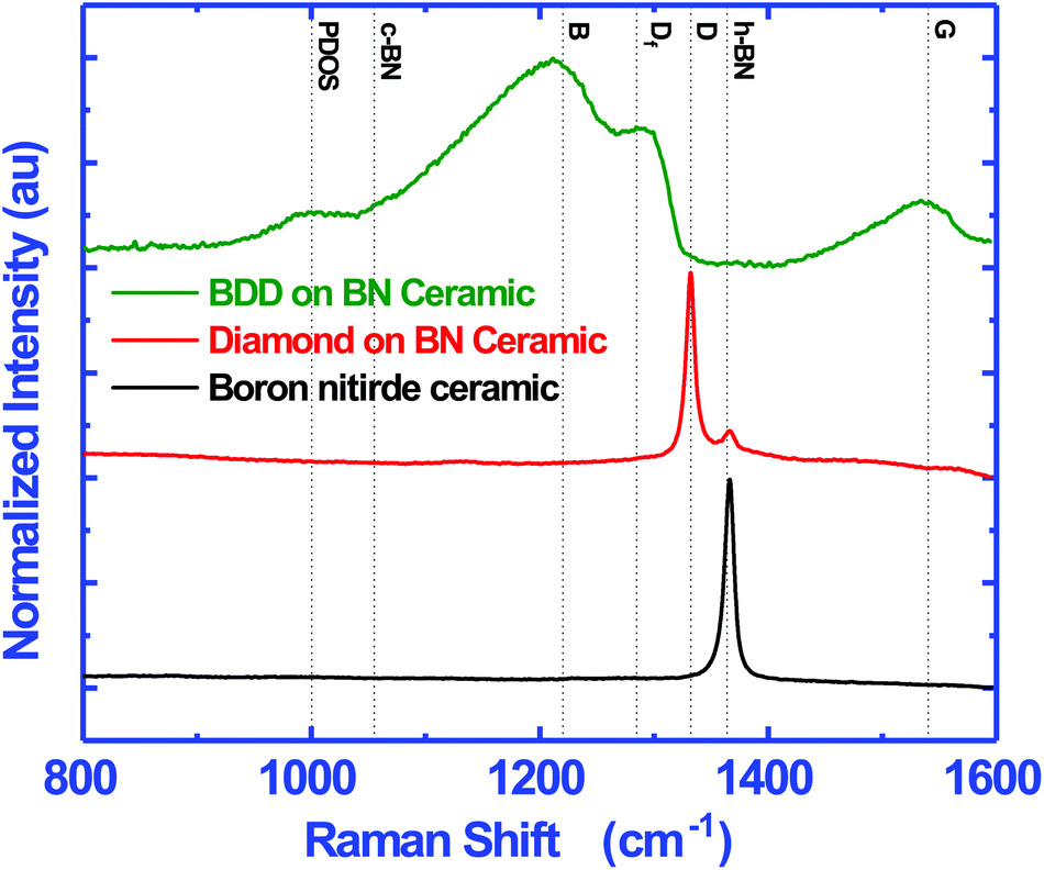 | ||
| Fig. 6 Raman spectra of the bare substrate (black), intrinsic nanocrystalline diamond (red) and boron doped nanocrystalline diamond (green) grown on BN ceramics. The dotted lines show the positions of various standard peaks. | ||
The film shows the regular characteristics of a heavily boron doped diamond with a broad band, B, peak at 1220 cm−1 and a shoulder DF at 1285 cm−1.29,44 Sidorov and Ekimov45 attribute the 1220 cm−1 peak to carbon–carbon bonding states. The addition of boron to diamond leads to a locally distorted lattice structure which can give rise to the band like structure46 and the intensity of the band is directly related to the doping level.47 The 1285 cm−1 shoulder is the red shifted diamond line from the characteristic 1332 cm−1 line seen in pure diamond. The Fano-like line shape of the diamond line is attributed to the quantum interference between the zone centre diamond phonon and the electronic states continuum introduced by the dopant.48–50 Furthermore, we can see a clear G band at 1560 cm−1 in the case of BDD while this is not present for undoped diamond. The G peak is due to the in-plane stretching of a pair of sp2 carbon sites.51–53 Commonly the G band is seen at 1580 cm−1 but it can appear anywhere between 1520–1580 cm−1.54 The shift in the G-band from 1580 cm−1 is mainly due to the sp2 site converting to the sp3 site when a π ring system converts to a π chain system.53 The absence of the G band in undoped diamond implies the high quality of the NCD film on the BN ceramic. Finally, a small shoulder at 1000 cm−1 can be seen which has been attributed to the maximum of phonon density of states (PDOSs) in diamond.44 This occurs due to the defects introduced by the dopant, allowing for the forbidden states to appear.55
3.4. Dielectric constant
We have measured the dielectric constant of the as received BN ceramics and the ceramics with undoped diamond grown on it. The measured dielectric constant of the pure boron nitride is frequency independent, with a nominal value of 4.2 ± 0.2 across the range of measurement. In addition, owing to its insulating nature, the loss is immeasurable with the measurement setup. The dielectric constant for the diamond-BN hybrid, measured through the material, increases to 46 ± 4. The dielectric loss also increases dramatically to give a frequency dependent value, implicit of free charge conductivity. For ceramic materials the dominant polarisation mechanism that contributes to the dielectric constant and loss, otherwise known as the complex permittivity, is electronic polarisation. This mechanism is associated with the displacement of the electron cloud distribution with respect to the nucleus which resonates out in the high terahertz region. This explains why the complex permittivity of the BN ceramic is frequency independent at kilohertz frequencies. Additionally, BN is not polar nor is it ionic since the B and N atoms share the same number of electrons, therefore, dipolar relaxation and ionic polarisation are not present. The immeasurable dielectric loss tangent is congruent with the insulating nature of h-BN owing to its high band gap energy. Even though sp2 bonded, the electrical properties of h-BN are unlike those of the carbon equivalent of graphite, where a high dielectric loss is expected owing to its high planar conductivity. After CVD diamond growth, there is a large increase in the dielectric constant. While the dielectric constant of diamond is approximately 5.6,16 the increase may be associated with Maxwell–Wagner–Sillars type interfacial polarisation.56 This model is normally used for explaining electrically conducting materials in a non-conducting medium; both h-BN and diamond are electrical insulators. In which case, very small concentrations of sp2 carbon may be present at the interface between the materials and therefore, the absence of sp2 carbon signatures in the Raman spectroscopy measurements is plausible.573.5. Superconductivity
Superconductivity in boron doped diamond58 is one of the many superlative properties of BDD. We have tested the superconducting properties of doped diamond on BN ceramics to see if this property is retained even when the material is grown on a ceramic. Fig. 7 shows the reduced resistance (R/R300 K) vs. temperature for a BDD film grown on BN ceramics. The transition temperature (Tc) of the film is ∼3.4 K and the transition width, ΔTc = 1 K. The inset in the same figure shows the reduced resistance vs. temperature of the sample between 2 and 300 K. Such behaviour has been seen in BDD films on silicon.27 As the film was grown on an insulating ceramic like BN, the superconductivity is primarily from the BDD layer. The transition temperature was determined as the temperature at which the resistance is 1% of the normal state resistance. The transition width is the temperature difference between the temperatures at which the sample resistance is 99% and 1% of the normal state resistance.29 Similar transition temperatures and width have been reported on BDD.28,58–60 From Fig. 7 it is clear that the superconducting BDD can be grown on the ceramic substrate. This technique of growing diamond on ceramics can be useful in areas where machinable dielectrics can form large scale devices, which can then be coated with a thin layer of BDD.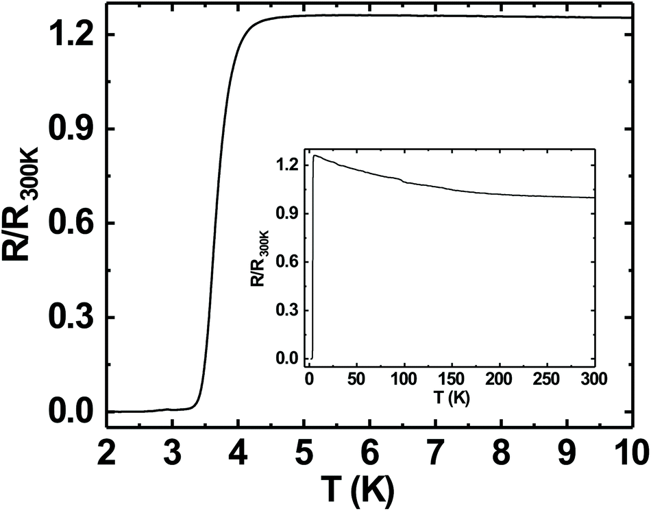 | ||
| Fig. 7 Reduced resistance vs. temperature of BDD grown on BN ceramics. The film shows a superconducting transition temperature at 3.5 K. Inset shows the reduced resistance vs. temperature of the sample between 2 and 300 K. | ||
Furthermore, we have also measured the critical field of the BDD layer. We have measured the resistance of the BDD layer as a function of the magnetic field at 2 K. The result of the measurement is presented in Fig. 8. The excitation current during the measurement was 5 μA. We have plotted the reduced resistance vs. field in the figure. For the calculation of reduced resistance the resistance at 300 K and zero magnetic field have been used as a reference. The red curve in the same figure is the first derivative of resistance. The right hand y-axis relates to the first derivative curve. From the curve we can see that the resistance starts increasing at ∼1.5 T and then plateaus at ∼3.5 T. The reduced resistance vs. temperature of the BDD layer at various applied magnetic fields has also been measured. The data were measured between 0 and 4.15 T with a field spacing of ∼0.15 T. The result of the experiment is shown in Fig. 9. The resistance of the film at 300 K and zero magnetic field have been taken as the reference for the calculation of reduced resistance. The inset in the figure shows the magnified view of the high field regime at low temperatures. It is clear from the figure that pockets of superconductivity exist at fields as large as 3.54 T. So, from Fig. 8 and 9 we can conclude that the critical field of the BDD layer at 2 K is between 1.5 and 3.5 T.
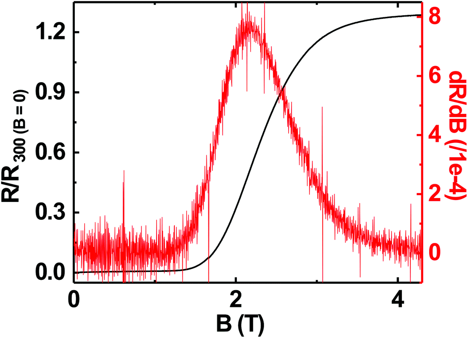 | ||
| Fig. 8 Reduced resistance vs. magnetic field has been plotted in this figure. The red curve is the first derivative of the reduced resistance vs. field curve. The right hand y-axis relates to the derivative curve. The temperature during the measurement was kept constant at 2 K. | ||
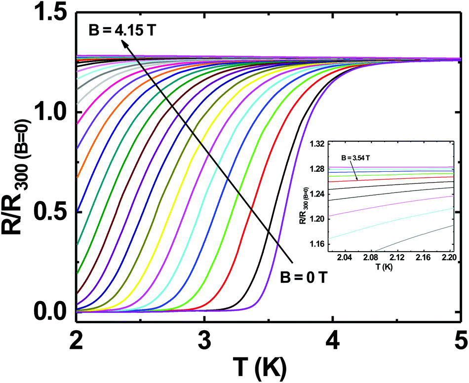 | ||
| Fig. 9 Reduced resistance vs. temperature at various applied magnetic fields has been plotted in this figure. The data were taken between 0 and 415 T with a field spacing of ∼0.15 T. The inset shows the magnified view of the high field regime at low temperatures. From the figure it can be seen that pockets of superconductivity exist at fields as large as 3.54 T. | ||
4. Conclusion
In conclusion, we have determined the ζ-potential of BN-ceramics. The ζ-potential is negative in the pH range of the diamond colloids used for seeding. The growth of diamond on the ceramic involves a pre-baking step due to the hygroscopic nature of the ceramic binding material. The quality of diamond as determined by Raman spectroscopy and SEM was found to be excellent. An increase in the dielectric constant from 4.2 ± 0.2 to 46 ± 4 was observed. Doped diamond grown on the ceramic retained its excellent superconducting properties.Dataset
The datasets generated and/or analysed during this study can be found at http://doi.org/10.17035/d.2019.0069330616.Conflicts of interest
There are no conflicts to declare.Acknowledgements
SM and OAW acknowledge financial support of the European Research Council (ERC) Consolidator Grant SUPERNEMS, Project ID: 647471. JAC acknowledge financial support of the Engineering and Physical Sciences Research Council under the program Grant GaN-DaME (EP/P00945X/1).References
- A. Lipp, K. Schwetz and K. Hunold, J. Eur. Ceram. Soc., 1989, 5, 3–9 CrossRef CAS.
- J. Thomas, N. E. Weston and T. E. O'Connor, J. Am. Chem. Soc., 1962, 84, 4619–4622 CrossRef CAS.
- A. Hérold, B. Marzluf and P. Pério, C. R. Acad. Sci., 1958, 246, 1866 Search PubMed.
- T. Ishii, T. Sato, Y. Sekikawa and M. Iwata, J. Cryst. Growth, 1981, 52, 285–289 CrossRef CAS.
- S.-I. Hirano, T. Yogo, S. Asada and S. Naka, J. Am. Ceram. Soc., 1989, 72, 66–70 CrossRef CAS.
- E. J. M. Hamilton, S. E. Dolan, C. M. Mann, H. O. Colijn, C. A. McDonald and S. G. Shore, Science, 1993, 260, 659–661 CrossRef CAS PubMed.
- R. Zedlitz, M. Heintze and M. Schubert, J. Non-Cryst. Solids, 1996, 198–200, 403–406 CrossRef CAS.
- W. H. Balmain, J. Prakt. Chem., 1842, 27, 422–430 CrossRef.
- K. M. Taylor, US Patent, 2808314, 1952 Search PubMed.
- R. Davis, Proc. IEEE, 1991, 79, 702–712 CrossRef CAS.
- R. Haubner, M. Wilhelm, R. Weissenbacher and B. Lux, High Performance Non-Oxide Ceramics II, Structure and Bonding, Springer, Berlin Heidelberg, 2002, vol. 102, pp. 1–45 Search PubMed.
- S. K. Lee, K. Nakamura, S. Kume and K. Watari, Mater. Sci. Forum, 2006, 510–511, 398–401 CAS.
- J. Eichler and C. Lesniak, J. Eur. Ceram. Soc., 2008, 28, 1105–1109 CrossRef CAS.
- F. Withers, T. H. Bointon, D. C. Hudson, M. F. Craciun and S. Russo, Sci. Rep., 2015, 4, 4967 CrossRef.
- A. Laturia, M. L. Van de Put and W. G. Vandenberghe, NPJ 2D Mater. Appl., 2018, 2, 6 CrossRef.
- S. Bhagavantam and D. A. A. S. Narayana Rao, Nature, 1948, 161, 729–729 CrossRef CAS.
- O. Williams, Diamond Relat. Mater., 2011, 20, 621–640 CrossRef CAS.
- W. D. Harkins, J. Chem. Phys., 1942, 10, 268–272 CrossRef CAS.
- M. Seth, S. G. Hatzikiriakos and T. M. Clere, Polym. Eng. Sci., 2002, 42, 743–752 CrossRef CAS.
- J. Hees, A. Kriele and O. A. Williams, Chem. Phys. Lett., 2011, 509, 12–15 CrossRef CAS.
- S. Yu, N. Yang, H. Zhuang, S. Mandal, O. A. Williams, B. Yang, N. Huang and X. Jiang, J. Mater. Chem. A, 2017, 5, 1778–1785 RSC.
- R. Van Wagenen and J. Andrade, J. Colloid Interface Sci., 1980, 76, 305–314 CrossRef CAS.
- A. Voigt, H. Wolf, S. Lauekner, G. Neumann, R. Becker and L. Richter, Biomaterials, 1983, 4, 299–304 CrossRef CAS PubMed.
- W. Norde and E. Rouwendal, J. Colloid Interface Sci., 1990, 139, 169–176 CrossRef CAS.
- P. J. Scales, F. Grieser and T. W. Healy, Langmuir, 1990, 6, 582–589 CrossRef CAS.
- S. Mandal, E. L. H. Thomas, C. Middleton, L. Gines, J. T. Griffiths, M. J. Kappers, R. A. Oliver, D. J. Wallis, L. E. Goff, S. A. Lynch, M. Kuball and O. A. Williams, ACS Omega, 2017, 2, 7275–7280 CrossRef CAS.
- G. M. Klemencic, S. Mandal, J. M. Werrell, S. R. Giblin and O. A. Williams, Sci. Technol. Adv. Mater., 2017, 18, 239–244 CrossRef CAS.
- G. M. Klemencic, J. M. Fellows, J. M. Werrell, S. Mandal, S. R. Giblin, R. A. Smith and O. A. Williams, Phys. Rev. Mater., 2017, 1, 044801 CrossRef.
- H. A. Bland, E. L. H. Thomas, G. M. Klemencic, S. Mandal, D. J. Morgan, A. Papageorgiou, T. G. Jones and O. A. Williams, Sci. Rep., 2019, 9, 2911 CrossRef.
- S. Leeds, T. Davis, P. May, C. Pickard and M. Ashfold, Diamond Relat. Mater., 1998, 7, 233–237 CrossRef CAS.
- J. A. Cuenca, S. Mandal, M. Snowball, A. Porch and O. A. Williams, under preparation, 2019.
- O. A. Williams, J. Hees, C. Dieker, W. Jäger, L. Kirste and C. E. Nebel, ACS Nano, 2010, 4, 4824–4830 CrossRef CAS PubMed.
- M. J. Crimp, D. A. Oppermann and K. Krehbiel, J. Mater. Sci., 1999, 34, 2621–2625 CrossRef CAS.
- J. Li, Y. Huang, Z. Liu, J. Zhang, X. Liu, H. Luo, Y. Ma, X. Xu, Y. Lu, J. Lin, J. Zou and C. Tang, J. Mater. Chem. A, 2015, 3, 8185–8193 RSC.
- P. D. Williams and D. D. Hawn, J. Am. Ceram. Soc., 1991, 74, 1614–1618 CrossRef CAS.
- J. A. Lewis, J. Am. Ceram. Soc., 2004, 83, 2341–2359 CrossRef.
- H. A. Girard, S. Perruchas, C. Gesset, M. Chaigneau, L. Vieille, J. C. Arnault, P. Bergonzo, J. P. Boilot and T. Gacoin, ACS Appl. Mater. Interfaces, 2009, 1, 2738–2746 CrossRef CAS PubMed.
- S. Mandal, E. L. H. Thomas, T. A. Jenny and O. A. Williams, ACS Appl. Mater. Interfaces, 2016, 8, 26220–26225 CrossRef CAS.
- S. Reich, A. C. Ferrari, R. Arenal, A. Loiseau, I. Bello and J. Robertson, Phys. Rev. B: Condens. Matter Mater. Phys., 2005, 71, 205201 CrossRef.
- C. Ramaswamy, Nature, 1930, 125, 704–704 CrossRef CAS.
- R. Robertson and J. J. Fox, Nature, 1930, 125, 704 CrossRef CAS.
- S. Bhagavantam, Indian J. Phys., 1930, 5, 169 Search PubMed.
- P. May, W. Ludlow, M. Hannaway, P. Heard, J. Smith and K. Rosser, Diamond Relat. Mater., 2008, 17, 105–117 CrossRef CAS.
- P. Szirmai, T. Pichler, O. A. Williams, S. Mandal, C. Bäuerle and F. Simon, Phys. Status Solidi B, 2012, 249, 2656–2659 CrossRef CAS.
- V. A. Sidorov and E. A. Ekimov, Diamond Relat. Mater., 2010, 19, 351–357 CrossRef CAS.
- P. Ashcheulov, J. Šebera, A. Kovalenko, V. Petrák, F. Fendrych, M. Nesládek, A. Taylor, Z. V. Živcová, O. Frank, L. Kavan, M. Dračínský, P. Hubík, J. Vacík, I. Kraus and I. Kratochvílová, Eur. Phys. J. B, 2013, 86, 12–18 CrossRef.
- P. May, W. Ludlow, M. Hannaway, P. Heard, J. Smith and K. Rosser, Chem. Phys. Lett., 2007, 446, 103–108 CrossRef CAS.
- E. Gheeraert, P. Gonon, A. Deneuville, L. Abello and G. Lucazeau, Diamond Relat. Mater., 1993, 2, 742–745 CrossRef CAS.
- J. W. Ager, W. Walukiewicz, M. McCluskey, M. A. Plano and M. I. Landstrass, Appl. Phys. Lett., 1995, 616, 616 CrossRef.
- F. Pruvost and A. Deneuville, Diamond Relat. Mater., 2001, 10, 531–535 CrossRef CAS.
- A. C. Ferrari and J. Robertson, Phys. Rev. B: Condens. Matter Mater. Phys., 2000, 61, 14095–14107 CrossRef CAS.
- A. C. Ferrari and J. Robertson, Phys. Rev. B: Condens. Matter Mater. Phys., 2001, 64, 075414 CrossRef.
- A. C. Ferrari and J. Robertson, Philosophical Transactions of the Royal Society A: Mathematical, Physical and Engineering Sciences, 2004, vol. 362, pp. 2477–2512 Search PubMed.
- S. Prawer and R. J. Nemanich, Philosophical Transactions of the Royal Society of London. Series A: Mathematical, Physical and Engineering Sciences, 2004, vol. 362, pp. 2537–2565 Search PubMed.
- S. Prawer, K. Nugent and D. Jamieson, Diamond Relat. Mater., 1998, 7, 106–110 CrossRef CAS.
- X. Xia, Z. Zhong and G. J. Weng, Mech. Mater., 2017, 109, 42–50 CrossRef.
- J. A. Cuenca, E. L. H. Thomas, S. Mandal, D. J. Morgan, F. Lloret, D. Araujo, O. A. Williams and A. Porch, ACS Omega, 2018, 3, 2183–2192 CrossRef CAS.
- E. A. Ekimov, V. A. Sidorov, E. D. Bauer, N. N. Mel'nik, N. J. Curro, J. D. Thompson and S. M. Stishov, Nature, 2004, 428, 542–545 CrossRef CAS.
- Y. Takano, M. Nagao, T. Takenouchi, H. Umezawa, I. Sakaguchi, M. Tachiki and H. Kawarada, Diamond Relat. Mater., 2005, 14, 1936–1938 CrossRef CAS.
- G. Zhang, T. Samuely, Z. Xu, J. K. Jochum, A. Volodin, S. Zhou, P. W. May, O. Onufriienko, J. Kačmarčík, J. A. Steele, J. Li, J. Vanacken, J. Vacík, P. Szabó, H. Yuan, M. B. J. Roeffaers, D. Cerbu, P. Samuely, J. Hofkens and V. V. Moshchalkov, ACS Nano, 2017, 11, 5358–5366 CrossRef CAS PubMed.
| This journal is © The Royal Society of Chemistry 2019 |