Electrostatics of metal–graphene interfaces: sharp p–n junctions for electron-optical applications†

Abstract
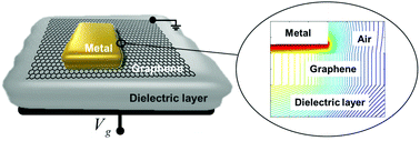
Creation of sharp lateral p–n junctions in graphene devices, with transition widths w well below the Fermi wavelength λF of graphene's charge carriers, is vital to study and exploit these electronic systems for electron-optical applications. The achievement of such junctions is, however, not trivial due to the presence of a considerable out-of-plane electric field in lateral p–n junctions, resulting in large widths. Metal–graphene interfaces represent a novel, promising and easy to implement technique to engineer such sharp lateral p–n junctions in graphene field-effect devices, in clear contrast to the much wider (i.e. smooth) junctions achieved via conventional local gating. In this work, we present a systematic and robust investigation of the electrostatic problem of metal-induced lateral p–n junctions in gated graphene devices for electron-optics applications, systems where the width w of the created junctions is not only determined by the metal used but also depends on external factors such as device geometries, dielectric environment and different operational parameters such as carrier density and temperature. Our calculations demonstrate that sharp junctions (w ≪ λF) can be achieved via metal–graphene interfaces at room temperature in devices surrounded by dielectric media with low relative permittivity (<10). In addition, we show how specific details such as the separation distance between metal and graphene and the permittivity of the gap in-between plays a critical role when defining the p–n junction, not only defining its width w but also the energy shift of graphene underneath the metal. These results can be extended to any two-dimensional (2D) electronic system doped by the presence of metal clusters and thus are relevant for understanding interfaces between metals and other 2D materials.
 Please wait while we load your content...

