
 Open Access Article
 This Open Access Article is licensed under a
 Creative Commons Attribution 3.0 Unported Licence
Propagation of amorphous oxide nanowires via the VLS mechanism: growth kinetics†
D.
Shakthivel
a,
W. T.
Navaraj
a,
Simon
Champet
b,
Duncan H.
Gregory
b and
R. S.
Dahiya
*a
aBendable Electronics and Sensing Technologies (BEST) Group, School of Engineering, University of Glasgow, G12 8QQ, UK. E-mail: Ravinder.Dahiya@glasgow.ac.uk
bWestCHEM, School of Chemistry, University of Glasgow, G12 8QQ, UK
First published on 17th July 2019
Abstract
This work reports the growth kinetics of amorphous nanowires (NWs) developed by the vapour–liquid–solid (VLS) mechanism. The model presented here incorporates all atomistic processes contributing to the growth of amorphous oxide NWs having diameters in the 5–100 nm range. The steady state growth condition has been described by balancing the key atomistic process steps. It is found that the 2D nano-catalyst liquid and NW solid (L–S) interface plays a central role in the kinetic analysis. The balance between the 2D Si layer crystallization and oxidation rate is quantitatively examined and compared with experimental values. The atomistic process dependencies of the NW growth rate, supersaturation (C/C0), desolvation energy (QD) barrier and NW diameter have been analyzed in detail. The model successfully predicts the reported NW growth rate to be in the range of 1–10 μm s−1. A novel seed/catalyst metal-based synthesis strategy for the preparation of amorphous silica NWs is reported. A nickel thin film on Si is used as a seed metal for the Au assisted VLS growth of silica NWs. The experimental results provide evidence of the creation of SiO under the given conditions followed by Si injection in the Au–Si nano-catalyst solution. The usage of seed metal was observed to reduce the growth temperature compared to the methods reported in the literature and obtain similar growth rates. The technique presented here holds promise for the synthesis of sub-100 nm diameter NWs.
1. Introduction
Inorganic nanowires (NWs) with diameters < 100 nm are widely studied as they hold great potential for nanoelectronics,1,2 sensors,3,4 flexible electronics,5–7 energy generation,8 energy storage,9,10etc., owing to their interesting physical and chemical properties.11–16 For example, the rapid change in the resistance of ZnO NWs with exposure to UV light makes them ideal for wearable dosimeters.17 Likewise, with photoluminescence (PL) bands in the range of 1.9–4.3 eV, the NWs of amorphous silica exhibit exciting optical properties, which could address the challenge related to blue light emission.18,19 Such properties are often exploited to develop novel sensors, IR detectors, efficient waveguides, etc. To this end, the NWs also require laborious tailoring of dimensions, growth processes, site-specific synthesis, etc. The task could be easier if there is a quantitative understanding of experimental conditions (e.g. temperature, pressure, etc.) during the NW growth process.In this regard, the catalyst particle-assisted vapour–liquid–solid (VLS) growth mechanism has been extensively studied and there is a good understanding about the mechanism in the crystalline context.6 Surprisingly, the growth of amorphous NWs using the VLS mechanism has never been explained even if this method has been used to produce amorphous NWs such as silica (SiOx) and germanium oxide (GeOx).20–22 This is surprising because a large experimental dataset is available for VLS-synthesised silica NWs and, barring a small number of semi-quantitative models, the growth process for amorphous NWs remains relatively ambiguous.23–25 Herein we address this issue with studies focussing on the growth kinetics of amorphous NWs and an evaluation of the crucial parameters that influence the NW growth rates.
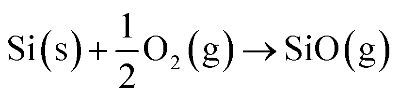
Silica NWs via the VLS method are typically grown at high temperature (>900 °C) by annealing Si sources (Si wafers, thin films and SiO powder) with nanoparticle catalysts (Au, Pt, Ni, etc.) under a flow of inert gas such as H2/N2 (forming gas), Ar or N2.26,27 The SiO vapours created in situ at these elevated temperatures act as the flux for NW growth.28,29 During the amorphous NW growth, these SiO vapours get adsorbed on Au catalyst particles and then Si species are injected into the bulk of the catalyst particles. Si injection leads to the formation of a nano Au–Si catalyst solution. When the Au–Si solution is supersaturated with Si, the growth of NWs is initiated at the catalyst–substrate 2D interface. This initiation of Si crystallization is attributed to the selective exclusion of oxygen molecules (or O2− ions) from the Au–Si catalyst solution because of the poor solubility of oxygen at high NW growth temperatures.30 The growth of amorphous SiOx (and GeOx) NWs starts when the oxygen atoms are directly incorporated at the catalyst-NW 2D interface and thereafter the coupled Si crystallization–oxidation process continues. Oxygen atoms get adsorbed at the vapour–liquid–solid triple phase boundary (TPB) and diffuse through the 2D interface for the oxidation process. The distinctive oxidation of Si crystals at this L–S interface is the key for amorphous NW growth. The interface-oxidation phenomenon is exclusive to NW growth, where oxidation occurs at the nano liquid–solid (L–S) interface,31 and is crucial in rationalising the VLS growth of amorphous NWs and their counterparts in crystalline metal-oxides (Al2O3, ZnO, etc.). The chemical composition of the catalyst solution (Au–Si) during this process also plays a crucial role in the synthesis of silica NWs.22,24
Taking the above established qualitative understanding as a basis, a kinetic model is presented here to explain the growth of amorphous NWs. The kinetic model is obtained from four atomistic steps:32,33 (1) Si species (i.e. SiO) generation and transportation, (2) Si incorporation into the catalyst particle, (3) Si crystallization at the interface, and (4) Si oxidation at the interface. Mathematical expressions have been developed for each of these steps to explain the steady state growth of NWs.33,34 The key feature of this work is the elucidation of the crystallization and oxidation processes occurring at the L–S interface. By using appropriate crystallization modes, the growth rate of NWs has been estimated with a range of kinetic parameters.35,36 The estimated growth rate has been found to be within the range of the experimentally measured values. The kinetic framework of the crystallization–oxidation phenomenon is verified by performing experiments under low oxygen partial pressure conditions. Si oxidation at the L–S interface is compared with the conventional vapour–solid oxidation of single crystal NWs.37,38 While the oxidation of crystalline Si NWs of 10–100 nm diameter takes from 30 min to 5 h, the direct growth of amorphous silica NWs of similar diameter can achieve lengths of several microns within 30 minutes. The kinetic model presented here shows a strong influence of the catalyst on the oxidation process at the L–S interface. The analogous case of amorphous GeOx nanowire growth is also considered (Fig. S1†).
2. Experimental work
Amorphous SiOx and GeOx NWs of diameter in the range of 5–100 nm were grown on silicon and stainless steel (SS) substrates using solid sources (Si wafers and Si and Ge thin films) to probe the atomistic steps of the VLS growth process. NW growth was performed in a resistance heating furnace under forming gas, 5% H2/N2 (99.99%, BOC), at 900 °C. Monocrystalline (100) p-type Si wafers were cleaned with acetone, isopropanol (IPA), and deionised (DI) water to remove surface contaminants. NWs were grown using bimetallic Ni/Au thin films to separate the monoxide vapours (SiO or GeO) and the catalyst particles from the solid source surface (Fig. 1). Two different Ni/Au bimetallic configurations have been prepared for NW synthesis (Fig. 1(a1 and a2)). Firstly, an Ni thin film typically of thickness 10–40 nm was deposited by e-beam evaporation. Subsequently, an Au thin film (3–5 nm in thickness) was deposited by sputtering onto the Ni surface (Fig. 1(a1)). Au films were annealed at 900 °C for 10 minutes under 5% H2/N2 to obtain statistically distributed catalyst nanoparticles of 5–100 nm in diameter (Fig. 1b). The Au film thickness plays a key role in determining the particle size distribution. Dewetted Au nano-particles (Fig. 1b) are produced by the film breaking at the grain boundaries where the grains are converted into particles.39,40 The average grain size in the Au thin films increases with thickness which has a direct impact on the resulting particle size distribution. The Ni thin film enhances SiO generation from the solid Si source (wafers and thin films) at 900 °C. The de-wetted Au nanoparticles act as a catalyst for NW synthesis by the VLS method. In the second Ni/Au configuration, the Ni and Au films were deposited in parallel on the Si surface to show that the SiO vapour is transported from the Ni/Si region to Au particles (Fig. 1(a2)). The flow reactor system used a quartz tube of 25 mm internal diameter. Si substrate samples of 1 cm2 area pre-deposited with Ni/Au films were placed in a quartz boat and loaded into the quartz tube reactor. In the case of the coplanar Ni/Au configuration, the substrate placement ensured that the Au layer was downstream of the Ni layer (i.e. that the gas flow would transport the anticipated SiO vapour towards the Au catalyst particles). The quartz reaction tube was sealed at both ends (gas inlet and outlet) with metal flanges equipped with O-rings and water cooling. The samples were heated to the synthesis temperature of 900 °C at a heating rate of 22 °C min−1 and were withdrawn after cooling to room temperature. SS deposited with Si films 1 μm in thickness were used as an alternative substrate and source for SiO vapour. The Si thin films were deposited on the SS substrate using PECVD (Oxford Instruments-Plasmalab 80+) followed by Ni and Au deposition as noted above for Si wafers.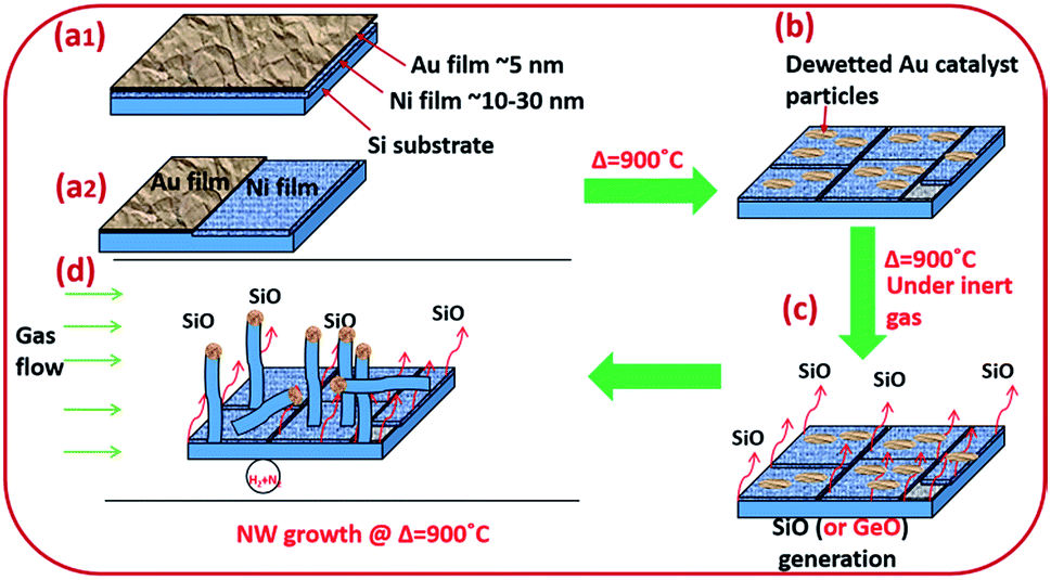 | ||
| Fig. 1 Schematic diagram of silica (or germania) NW synthesis. (a1) Si (or Ge)/Ni/Au stack configurations; (a2) Ni/Au bimetallic film deposited in parallel configuration; (b) de-wetted Au films, creating Au nanoparticles 5–100 nm in diameter; (c) generation of SiO gas; (d) site-specific growth of SiOx or GeOx NWs at Au nanoparticle sites. | ||
Amorphous GeOx NWs were synthesised under similar conditions to those described above except that Ge thin films (50 nm thick) were used by depositing Ge on an Si substrate by e-beam evaporation (ESI Section S1†). In additional experiments we explored the synthesis of silica NWs under low oxygen partial pressure conditions in a vacuum-sealed quartz tube. These experiments were performed to investigate the crystallization phenomenon at the catalyst/NW interface further. Low oxygen partial pressure was expected to prevent the oxidation of crystallized Si at the L–S interface. In a typical experiment an Si wafer coated with Ni/Au was sealed inside a quartz tube of 15 mm diameter under vacuum (10−3 Torr). The sealed tube was heated to 900 °C for 30 minutes to synthesize silica NWs.
SiO2 and GeO2 NWs synthesised via all the methods described above were characterised by Scanning Electron Microscopy (SEM-FEI Nova NanoSem 630) and Transmission Electron Microscopy (TEM-FEI Technai T20). NWs were mechanically removed from the substrate and dispersed in DI water for sonication. NWs were transferred to carbon-coated TEM grids for imaging. Bright field and HRTEM images were recorded under an operating potential of 200 keV.
3. Results and discussion
3.1. Silica NWs using Si wafers and thin Si films with Ni/Au stacks
Silica NWs were synthesised on Si wafers and SS substrates deposited with Ni/Au at 900 °C (Fig. 2 and 3). The first objective of these experiments was to verify that NW growth occurs only at the Au catalyst particle sites (from SiO vapours created in situ). De-wetting of the thin film was used to produce Au particles of 5–100 nm diameter at 900 °C (Fig. 2a). SEM images of the resulting silica NWs grown under these conditions are shown in Fig. 2b and c. The diameters of the NWs closely match with the dimensions of the Au nanoparticles, implying not only that growth occurs at the Au catalyst particle sites, but also that the diameter of the wires is expressly directed by the size of the Au particles (Fig. 2c). Based on Fig. 1 and 2, the SEM images indicate the two-fold utility of Ni films in the NW growth process: (1) promoting lower temperature VLS growth (at 900 °C and likely via SiO vapour generation in situ) and (2) providing physical separation between the NWs and the Si wafer to probe the growth kinetics. Previous studies have shown that SiOx NWs are typically grown on Au-coated Si wafers at or above 1000 °C.26,41 Our experiments demonstrate, however, that growth of amorphous SiOx and GeOx NWs (ESI, S1†) is possible at lower temperature (<1000 °C). The use of Ni film has been extended to enable silica NWs to be synthesised on a stainless steel (SS) (3 mm thick, 304 L) substrate. A thin film of polycrystalline Si (thickness – 1 μm) was deposited using the PECVD technique on the SS substrate followed by Ni/Au stacking by evaporation. The polycrystalline Si film served as the Si source for SiOx NWs. SEM images in Fig. 2d–f show SiOx NWs grown on an SS substrate at 900 °C. The presented data suggest that NW growth using Si films on an SS substrate occurs just as it does on Si wafers via a VLS mechanism from SiO vapour. These results are especially promising in demonstrating the range of Si-coated substrates that could be available for silica NW growth. Clearly such substrate combinations could be selected depending on the foreseen applications. PECVD deposited Si films were observed to attach weakly to the SS substrate. A prolonged growth duration could result in a freestanding mesh of silica NWs.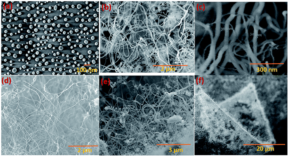 | ||
| Fig. 2 SEM images of silica NWs grown at 900 °C using Si wafers and Si thin films on an SS substrate. (a) Au catalyst nanoparticles prepared by de-wetting; (b and c) NWs grown using the Ni/Au catalyst and SiO source on an Si wafer; (d and f) silica NWs grown using PECVD of an Si film (1 μm thick) on the SS substrate. (f) SEM image showing an edge of the SS substrate covered with NWs. | ||
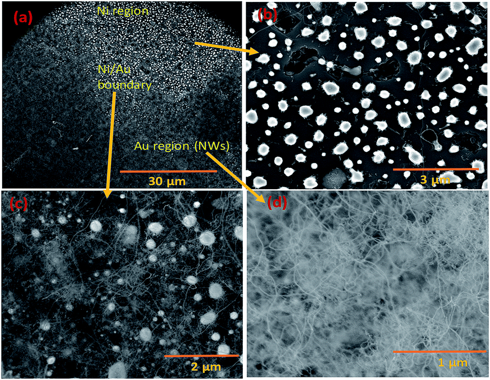 | ||
| Fig. 3 SEM images of Si NWs grown with Ni and Au in coplanar configuration. (a) Enlarged view shows both Ni and Au regions; (b) Ni particles without NWs; (c) region close to the interface between Au and Ni; and (d) silica NWs in the Au-deposited region. | ||
The Ni and Au films deposited in a coplanar configuration on a 1 cm2 Si wafer by hard masking are shown as a schematic in Fig. 1a. The localization of an Ni layer (in its role as the initiator of SiO vapour formation) and Au layer as a catalytic surface for NW growth was tested with this arrangement and the results are shown in Fig. 3. The three unique surface regions so-created are shown in detail in Fig. 3b: Ni film fragments; Fig. 3c: the Ni–Au interface region and Fig. 3d: the Au particle region post-NW growth (which is restricted to the regions containing Au). The SEM images indicate that SiO vapour was likely predominantly created in the Ni region and was transported and adsorbed over Au catalyst particles. The Au catalyst particles were positioned upstream of the forming gas. The SiO vapours generated in situ would thus be transported from the Ni layer to the Au. As shown in Fig. 3b, the 10 nm Ni film fragments form discrete nanoparticles during the heating process. The thickness of the Ni films used was optimized to 10–40 nm. This range of thickness was necessary for NW growth (with additional observable variations in the Ni film morphology due to temperature effects). The 10 nm Ni film was broken into droplets (such as those shown in Fig. 3b) whereas 40 nm thick films stayed intact. Distinct regions over an area of the substrate could thus be discerned where the SiO flux had been transported from the Ni film to the regions containing the Au catalyst particles.
Given the experimental conditions used in this work, there are two reasons for the poor performance of Ni as a catalyst compared to the Au metal particles: (1) the Ni particles tend to form a thin oxide (NiOx) layer on the surface even under low oxygen and partial pressure conditions. This oxide layer prevents flux (SiO and GeO in this case) injection through the surface. The Ni metal is used for the growth of single crystal NWs (Si, Ge etc.) by the VLS mechanism under controlled ambient conditions, where pure H2 is used as the carrier gas. In this case, the formation of NiO is controlled by the lack of oxygen. (2) The Ni catalyst goes through many phase transformations compared to the Au, as shown in the Ni–Si42 and Au–Si43 binary phase diagrams below. The formation of an Ni–Si solution is feasible only above 1000 °C. However, as a noble metal, Au behaves as a catalyst above 363 °C without any problem of native oxide formation on the nanoparticle surface. Given the experimental conditions, SiO flux is preferentially absorbed by Au particles rather than by the Ni surface. The binary phase diagrams are presented in ESI Section S2.†Fig. 3b shows that a small number of NWs emerge from Ni particles. NW “bunches” from (larger) catalyst particles have been reported in the literature to grow from low melting metals such Ga and Sn.22,27,44 The existence of many of such NW “bunches” have been explained by invoking solid–liquid–solid (SLS) growth mechanisms, without considering the role of vapour generation. Depending on the experimental conditions, the silica NWs could be produced by any of the three mechanisms45 shown in Fig. S3-1.† The different mechanistic pathways described in the literature to explain these growth modes have been unified in this work in terms of a single kinetic framework. A common aspect of the growth modes shown in Fig. S3-1† is the existence of a L–S interface between the catalyst droplet and the emerging NWs. The creation mechanism of these various L–S interfaces may vary with experimental conditions. For example, in the case of bunched NWs, the relatively large catalyst particles precipitate NWs at various locations due the attainment of local supersaturation. The L–S interface acts as a sink for the supersaturated catalyst particles and the liquid catalyst solution continues to attract flux from the vapour for continuous NW growth. As shown in Fig. 3b, a relatively small number of NWs are located at the Ni particle sites. Given the relatively low temperature employed and the availability of Au particles in the close vicinity, the SiO flux is presumably preferentially ad/absorbed at the Au catalyst particle sites as compared to the larger sized Ni. The dissolved Si will tend to precipitate as crystallites at the L–S interface; we have studied this phenomenon in more detail by TEM as described more fully below (Section 3.1.1). It is proposed that elemental Si repeatedly crystallizes at the interface followed by rapid oxidation leading to prolonged NW growth. Analysis of the TEM micrographs of silica NWs grown under the described conditions did not reveal crystalline Si at the interface, however (Fig. 4b), this could be due to the relative timescales of Si crystallization and the subsequent oxidation and growth phenomena, which would be expected to perhaps range from milli- to micro-seconds. In view of the timescales of these processes, NW growth under low oxygen pressure conditions (Fig. 4) was attempted with the intent of separating and analysing the crystallization–oxidation processes.
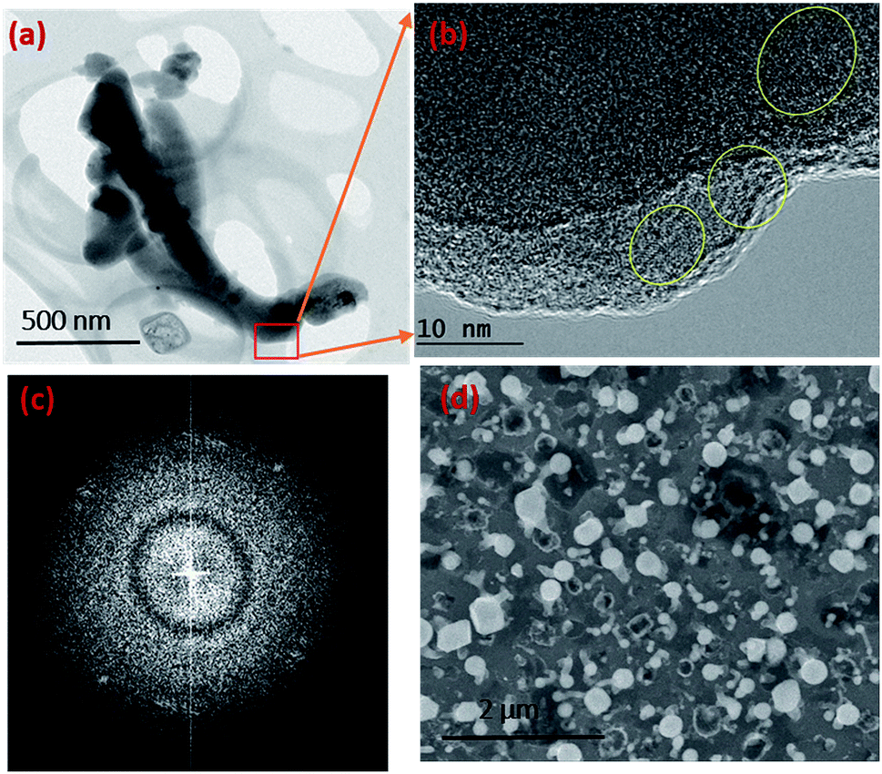 | ||
| Fig. 4 TEM and SEM images of silica NWs grown in a sealed quartz tube. (a) BF TEM image of NWs grown for 30 minutes. (b) Si crystallites encircled at the edges of NWs of image (a) where large parts are amorphous. (c) FFT pattern of the TEM image in (b) showing the diffraction spots arising from Si crystallites. The large diffuse rings prove that the NW is largely amorphous. (d) SEM image of the silica NWs over an area. | ||
3.2. Development of the kinetic model
| H2 (g) + SiO2 (s) → 2SiO (g) + H2O (g) | (1) |
This reaction is driven by H2 reduction of thermally grown SiO2 to create SiO vapours. Further, two additional pathways to produce SiO gaseous species are:
| Si (s) + SiO2 (s) → 2SiO (g) | (2) |
 | (3) |
Reactions (2) and (3) describe the pathways of SiO creation that are possible under the flow of inert gases such as Ar, N2 and O2, where Si can react with amorphous oxide and O2 gas (at low partial pressure in the feed gas). However, metal films also influence the generation of SiO vapour. Results here and elsewhere show that deposited metal films of Au or Ni of thickness in the range of 1–20 nm break into droplets and can alloy with Si.48 The liquid droplets, Au–Si or Ni–Si could also contribute to the creation of SiO vapours, and Si atoms vaporizing from these liquid solutions would tend to produce SiO vapour. The contribution of SiO formed via this metal-assisted mode towards NW growth has not been reported before. This could be attributed to the low vapour pressure of Si on Au–Si under conventional experimental conditions. The evaporation of Si from metal melts (Au–Si and Ni–Si) contributes the lowest compared to steps (1)–(3). The possibility of SiO generation in a system with Ni and Au deposited in a coplanar configuration was studied in this work with the intention of identifying the contribution of each metal. Results suggest that Ni enhances SiO generation while Au catalyses NW growth. In summary, all of the three possible mechanisms defined by eqn (1)–(3) along with the alternative of Si vaporisation could contribute to creation of SiO vapour for NW growth.
| 2SiO (g) → 2Si (ads) + O2 (g) | (4) |
Microscopically, the Au catalyst particles are converted into an Au–Si solution by dissolving Si from the substrate at and above a temperature of 363 °C, in accordance with the binary phase diagram. The rate of incorporation of Si into the droplet could be derived using Langmuir–Hinshelwood kinetics as:34
 | (5) |
 | (6) |
| Rcrystallization = (Jπr2)a | (7) |
 | (8) |
 | (9) |
 is the derivative of a zero order Bessel function. The second term of this solution consists of a Bessel function. The time required to attain oxygen saturation could be obtained using eqn (9). The exact value of the diffusivity of oxygen at the Au–Si/silica interface is not available in the literature. The coefficient of interface diffusion is expressed as δDv and has value of 1.1 × 10⁻¹⁹ (m3 s−1) in the case of a liquid Al/Al2O3 interface.
| Rinjection = Rejection | (10) |
Generally, the ejection rate of an atomic flux is equal to the growth rate of the NWs. In silica (GeOx) NW growth, the ejection rate is equal to the rate of oxidation of silicon (germanium). The steady state condition for amorphous NW growth is expressed as:
| Rinjection(SiO) = Rejection (crystallization) = Roxidation | (11a) |
The injection step, composed of vapour phase saturation from SiO sources, occurs in situ on the Si substrate. This gas phase concentration is highly dependent on the synthesis temperature which is varied between 900 and 1000 °C. The local partial pressure of SiO molecules on an Au–Si droplet dictates the rate of Si injection into the droplet. The kinetic parameters of the SiO adsorption on an Au–Si droplet are unavailable in the literature.
Hence, the current model will evaluate the steady state by considering the mechanistic processes that occur in the condensed phases. During the steady growth of NWs,
| Rejection (crystallization) = Roxidation | (11b) |
The assessment of this condition using the outlined equations provides insight into an amorphous NW growth process involving two elements (Si and O). The supersaturated concentration (C) of Si in the Au–Si catalyst particle plays a vital role in the whole growth process as the driving force for crystallization. Measurement of the Si concentration in a nano Au–Si catalyst is both challenging and tedious with existing experimental tools such as TEM-EELS. An estimation of the ratio (C/C0) between the actual concentration and the equilibrium concentration (C0) could be obtained from the binary Au–Si phase diagram. Estimates of the range of C/C0 are essential to evaluate the growth rate of NWs. The estimated growth rate of NWs will be correlated with the lateral oxidation rate. An understanding of the steady state condition will enable the relative significance of each of the atomistic kinetic parameters involved in the amorphous NW VLS growth process to be assessed.
3.3. Kinetic model: results and discussion
The growth model aims to elucidate how the growth rate of amorphous NWs grown using the VLS mechanism depends on each of the factors outlined above. Growth of silica NWs using an Au catalyst is considered in this model for a particle size/NW range of 10–100 nm diameter. The steady state growth rate of NWs was estimated for temperatures of 900 °C and 1000 °C and the values were compared with literature reports. This temperature regime was chosen given (1) that such moderate temperature ranges have produced silica NWs at reasonable growth rates experimentally and (2) the stability of Au–Si in the liquid phase over this range as reflected by the Au–Si binary phase diagram. The steady state condition (eqn (11a)) consists of two interrelated sequential mechanistic pathways leading to amorphous NWs. The Si layer LL mode crystallization rate (LHS of eqn (11a)) was calculated and equated with the oxidation rate. The effect of kinetic parameters associated with these atomistic processes has been evaluated. | ||
| Fig. 5 Estimated 2D Si crystallization rate with variation of supersaturation between 1.2 and 1.5 at 900 °C for QD-10 kT. | ||
 | ||
| Fig. 6 Variation of saturation time of oxygen as a function of interface radius for saturation levels (C/Cs) of (a) 0.75 and (b) 0.999. | ||
Based on these estimates, the Si crystallization rate (nm s−1) can vary by several orders of magnitude with an increase in supersaturation from 1.1 to 1.5. The experimental silica growth rates can be deduced to vary between 0.5 and 1 μm s−1 from an analysis of the literature.26 Given the curved and entangled nature of the amorphous NWs grown under the experimental conditions reported herein and the difficulty in obtaining precise lengths, these values are derived from approximate length estimates in the literature. Currently, an attempt has been made to deduce the experimental growth rate of silica NWs and compare the range with growth rates predicted by the kinetic model. NWs have been grown for different durations (few minutes to 60 minutes) and their cross-sectional length measurement (ImageJR software tool) has been used to obtain the NW growth rate. The measured average growth rate of NWs is found to be 650 nm s−1. Given the entanglement issue with amorphous NWs, this estimate could be the lower bound of the growth rate. However, this falls well within the range of the parameters, C/C0-1.5 and QD-10, as shown in Fig. 5. This study helps to validate the developed kinetic model. Exact details of this characterization are presented in ESI Section 8 (S8†). As illustrated in Fig. 5, the crystallization rate falls in the range of 0.5–1 μm s−1 for C/C0 values of 1.4 and 1.5. The possible range of C/C0 values for the Au–Si binary system at 900 °C is between 1 and 2.3 with an equilibrium concentration of 42 at% of Si.35,36 In comparison, single crystal Si NWs that grow by the VLS mechanism using Si gaseous precursors (SiCl4 and SiH4) propagate at rates of 1–100 nm s−1,32,43 5–10 times lower in magnitude than the growth rate of amorphous SiOx NWs. The values of C/C0 have been estimated to vary between 1.1 and 1.3 maximum.34 The high growth rates could be attributed to localized processes that dominate the amorphous NW growth. The SiO molecular species created in situ during the growth process enhance the injection of Si into the catalyst particle as compared to the case of crystalline Si. In Si NW growth, Si vapour (from liquid SiCl4) and gas sources (silane) is diluted (1–10%) during supply. Under vapour phase transport conditions, more than 80% of these sources pass without reacting at the catalyst surface. As a result, the flux diluted 10–20% effectively contributes to growth. Compared to this scenario, silica growth under ambient conditions has a rich SiO source, which is probably one of the reasons for the higher order growth rate compared to that of Si NWs. This suggests that the steady flux injection–ejection is different for single crystal (Si) and amorphous (SiOx) NW growth processes. The estimates of the crystallization rate at 1000 °C are given in Section 3 of the ESI.†
 | ||
| Fig. 7 (a and b) Oxidation rate of crystallized 2D Si layers under two saturation conditions (0.75 and 0.99); (c) crystallization rate of Si 2D crystals at 900 °C. | ||
The crucial parameter which determines the oxygen transport is the interfacial diffusivity (Dv). Levi et al. defined an interface diffusion co-efficient, δDv = 1.1 × 10⁻¹⁹ (m3 s−1), for oxygen diffusion at a liquid Al/Al2O3 interface at 1100 °C,51 where δ is the interfacial width. A range of δDv values from 1 × 10⁻¹⁹ to 1 × 10⁻²¹ m3 s−1 is used in the current analysis of oxygen diffusion at the Au–Si/silica interface. Oxygen diffusion parameters at the Au–Si/silica 2D nano interface have not been studied through experiments or modelling. Fig. 6 shows the time required to attain oxygen saturation at the interface with a radius varying between 10 and 50 nm. The interfacial thickness of the Au–Si/silica interface, δ, is adjusted between 0.25 and 1 nm for oxygen saturation fractions of 0.75 (Fig. 6a) and 0.99 (Fig. 6b). The saturation time in the given diameter range varies from 0.01 ms to 0.3 ms for an oxygen saturation fraction of 0.75 and 0.999, respectively. Molecular O2 desorption should be minimal once oxygen steadily diffuses at the interface. The current scenario is different compared with the conventional Si wafer oxidation which occurs at the vapour–solid (V–S) interface. Oxygen desorption is common in V–S interface processes as the surface diffusion mechanism contributes significantly to the conversion of single crystal Si into amorphous silica. Under low oxygen partial pressures, this might lead to porous non-stoichiometric silica. The results of the silica NW characterization through EDX and EELS techniques showed that the Si![[thin space (1/6-em)]](https://www.rsc.org/images/entities/char_2009.gif) :O ratio is 1:1.6.23,25 The oxygen saturation approximation (>0.75) considered in this model ensures that the silica NWs with Si:O stoichiometry falls in the measured range.
:O ratio is 1:1.6.23,25 The oxygen saturation approximation (>0.75) considered in this model ensures that the silica NWs with Si:O stoichiometry falls in the measured range.
Fig. 7 compares the oxidation (a and b) and crystallization (c) rates under different growth parameters at 900 °C. These estimated crystallization and oxidation rates cover a wide range from 0.01 to >10 μm s−1 for the used thermodynamic and kinetic parameters. The oxidation and crystallization rates encompass the experimentally deduced silica growth rates in the range of 0.5–1 μm s−1. This shows that the oxidation rate of a crystalline Si layer is approximately the same order of magnitude as that of the NW crystallization process (Fig. 7c). This suggests that coupled dynamics of the processes at the interface decide the growth rate of amorphous NWs. It is evident that the saturation time is proportional to the interfacial area. The saturation fraction could influence the stoichiometry of the NWs. The overlap of the rate vs. radius plots in Fig. 7a and b shows that the interface layer width, δ, does not significantly influence the oxidation rate. The trends in the crystallization and oxidation rates are inversely related due to the different origin of these processes. The crystal growth of the Si layers is driven by existing supersaturation in the Au–Si droplet, whereas the oxidation occurs with a constant supply of oxygen molecules across the interface. The thickness of the growing crystalline 2D Si layer could vary from one monolayer to multiple atomic layers and this will depend entirely on the level of supersaturation. From the estimated growth rates (1–10 μm s−1), the time scale to grow a monolayer of Si (thickness 2.7 × 10⁻¹⁰ m) at the interface varies from 0.27 ms to 20 μs. The timescale, dimensions and operating temperature make it difficult to study such events using experimental tools. The oxidation process, which is modelled here as the concentration gradient-driven oxygen diffusion from the TPB to the central point of the interface, tends to create layers of oxygen molecules at the interface. The 2D Si crystallization occurs through mono- and poly-centre nucleation at the interface.53 Previous analysis considered that polycentre nucleation increases with the diameter of NWs and is attributed to the increased interfacial area.51 It is expected that the oxidation process could occur simultaneously during multiple nucleation events. The L–S interfacial oxidation process is very different compared to the V–S “active” oxidation of a pre-formed crystalline NW. Single crystal Si NWs have been oxidized by O2 gas at high temperature and modelled using conventional tools.38 The L–S interfacial oxidation timescale calculated here is 4–5 orders of magnitude faster than the V–S oxidation of single crystal NWs described previously.37 V–S NW oxidation occurs over a similar duration to that seen for bulk Si wet/dry oxidation (typically 30–120 minutes). The oxide thickness is limited by temperature. Similarly, when single crystal Ge NWs grown using an Au catalyst are heated between 325 and 450 °C under oxygen the product is amorphous GeOx NWs.54 In this case, the Au catalyst promoted the formation of a Au–Ge eutectic solution, followed by the diffusion of Ge atoms across the catalyst particle. This would also suggest that 2D crystallization followed by oxidation is required for the formation of amorphous NWs.
4. Conclusions
Synthesis of amorphous silica and germanium oxide NWs in the diameter range of 10–100 nm has been studied experimentally, and a phenomenological kinetic model has been developed for their synthesis via the VLS mechanism. A steady state model was adopted to incorporate all mechanistic pathways contributing to the NW growth. Importantly, the analysis shows that elemental Si is injected through a nano Au–Si catalyst solution and that oxygen diffuses through the TPB interface for amorphous SiOx NW propagation. The dynamic equilibrium between Si crystallization and oxidation is analysed with a range of thermodynamic (supersaturation) and kinetic parameters. The ongoing nature of Si injection, supersaturation, 2D crystallization and oxidation establishes a steady growth of NWs. The growth rate (0.5–1 μm s−1) of silica NWs was estimated for a diameter range of 10–100 nm and temperatures of 900 °C and 1000 °C. The experimentally measured growth rate of silica NWs is found to be 650 nm s−1, which closely matches with the growth rate predicted by the kinetic model. The growth rate is shown to be sensitive to the Si concentration in the Au–Si droplet. This model also shows that the oxidation occurring at the nano L–S interface is a different process from the V–S oxidation of crystalline NWs at high temperature. Oxidation of 2D Si layers is observed to occur in microseconds as compared to the V–S oxidation which requires hour timescales to complete. Synthesis of silica and GeOx NWs was also performed to test the kinetic model. The role of SiO vapour in the NW synthesis and growth process was confirmed by physically separating Si/Ge sources from catalyst particles, and the growth of silica NWs under reduced oxygen partial pressures demonstrated that the crystallization process occurs at the L–S interface rather than via a post-growth V–S oxidation of crystalline elemental NWs.Conflicts of interest
There are no conflicts to declare.Acknowledgements
This research was supported by the EPSRC Fellowship for Growth – PRINTSKIN (EP/M002527/1) and neuPRINTSKIN (EP/R029644/1) projects.References
- Y. Huang, X. Duan, Y. Cui, L. J. Lauhon, K.-H. Kim and C. M. Lieber, Science, 2001, 294, 1313–1317 CrossRef CAS PubMed.
- Y. Li, F. Qian, J. Xiang and C. M. Lieber, Mater. Today, 2006, 9, 18–27 CrossRef CAS.
- E. Comini and G. Sberveglieri, Mater. Today, 2010, 13, 36–44 CrossRef CAS.
- W. Taube Navaraj, C. García Núñez, D. Shakthivel, V. Vinciguerra, F. Labeau, D. H. Gregory and R. Dahiya, Front. Neurosci., 2017, 11, 501 CrossRef.
- K. Takei, T. Takahashi, J. C. Ho, H. Ko, A. G. Gillies, P. W. Leu, R. S. Fearing and A. Javey, Front. Neurosci., 2010, 9, 821 CAS.
- D. Shakthivel, C. G. Núñez and R. Dahiya, Inorganic Semiconducting Nanowires for Flexible Electronics, United Scholars Publication, USA, 2016 Search PubMed.
- R. Dahiya, Proc. IEEE, 2019, 107, 247–252 Search PubMed.
- B. Tian, X. Zheng, T. J. Kempa, Y. Fang, N. Yu, G. Yu, J. Huang and C. M. Lieber, nature, 2007, 449, 885 CrossRef CAS PubMed.
- C. K. Chan, H. Peng, G. Liu, K. McIlwrath, X. F. Zhang, R. A. Huggins and Y. Cui, Nat. Nanotechnol., 2008, 3, 31 CrossRef CAS PubMed.
- C. García Núñez, L. Manjakkal and R. Dahiya, npj Flexible Electronics, 2019, 3, 1 CrossRef.
- L. Tong, R. R. Gattass, J. B. Ashcom, S. He, J. Lou, M. Shen, I. Maxwell and E. Mazur, Nature, 2003, 426, 816 CrossRef CAS PubMed.
- J. Lou, L. Tong and Z. Ye, Opt. Express, 2005, 13, 2135–2140 CrossRef CAS PubMed.
- Z. L. Wang, R. P. Gao, J. L. Gole and J. D. Stout, Adv. Mater., 2000, 12, 1938–1940 CrossRef CAS.
- C. G. Núñez, F. Liu, W. T. Navaraj, A. Christou, D. Shakthivel and R. Dahiya, Microsyst. Nanoeng., 2018, 4, 22 CrossRef PubMed.
- C. García Núñez, W. T. Navaraj, F. Liu, D. Shakthivel and R. Dahiya, ACS Appl. Mater. Interfacesc, 2018, 10, 3058–3068 CrossRef PubMed.
- C. García Núñez, F. Liu, S. Xu and R. Dahiya, Integration Techniques for Micro/Nanostructure-Based Large-Area Electronics (Elements in Flexible and Large-Area Electronics), Cambridge University Press, Cambridge, 2018 Search PubMed.
- C. G. Núñez, A. Vilouras, W. T. Navaraj, F. Liu and R. Dahiya, IEEE Sens. J., 2018, 18, 7881–7888 Search PubMed.
- A. Kaushik, R. Kumar, E. Huey, S. Bhansali, N. Nair and M. Nair, Microchim. Acta, 2014, 181, 1759–1780 CrossRef CAS PubMed.
- D. Yu, Q. L. Hang, Y. Ding, H. Zhang, Z. Bai, J. Wang, Y. Zou, W. Qian, G. Xiong and S. Feng, Appl. Phys. Lett., 1998, 73, 3076–3078 CrossRef CAS.
- F. Kolb, H. Hofmeister, R. Scholz, M. Zacharias, U. Gösele, D. Ma and S.-T. Lee, J. Electrochem. Soc., 2004, 151, G472–G475 CrossRef CAS.
- A. Shalav, G. H. Collin, Y. Yang, T. Kim and R. G. Elliman, J. Mater. Res., 2011, 26, 2240–2246 CrossRef CAS.
- C.-H. Hsu, S.-Y. Chan and C.-F. Chen, Jpn. J. Appl. Phys., 2007, 46, 7554 CrossRef CAS.
- I. Aharonovich, Y. Lifshitz and S. Tamir, Appl. Phys. Lett., 2007, 90, 263109 CrossRef.
- J. L. Elechiguerra, J. Manriquez and M. Yacaman, Appl. Phys. A: Mater. Sci. Process., 2004, 79, 461–467 CrossRef CAS.
- P. K. Sekhar, S. N. Sambandam, D. K. Sood and S. Bhansali, Nanotechnology, 2006, 17, 4606 CrossRef CAS PubMed.
- A. Shalav, T. Kim and R. G. Elliman, IEEE J. Sel. Top. Quantum Electron., 2011, 17, 785–793 CAS.
- L. Zheng, B. Huang, J. Wei and Y. Dai, Mater. Lett., 2012, 80, 141–144 CrossRef CAS.
- R. Walkup and S. Raider, Appl. Phys. Lett., 1988, 53, 888–890 CrossRef CAS.
- A. Gomez-Martinez, F. Marquez and C. Morant, Appl. Surf. Sci., 2015, 345, 44–48 CrossRef CAS.
- D. Bahloul-Hourlier and P. Perrot, J. Phase Equilib. Diffus., 2007, 28, 150–157 CrossRef CAS.
- S. H. Oh, M. F. Chisholm, Y. Kauffmann, W. D. Kaplan, W. Luo, M. Rühle and C. Scheu, Science, 2010, 330, 489–493 CrossRef CAS.
- E. Givargizov, J. Cryst. Growth, 1975, 31, 20–30 CrossRef CAS.
- V. Schmidt, S. Senz and U. Gösele, Phys. Rev. B Condens. Matter Mater. Phys., 2007, 75, 045335 CrossRef.
- D. Shakthivel and S. Raghavan, J. Appl. Phys., 2012, 112, 024317 CrossRef.
- D. Shakthivel, S. Rathkanthiwar and S. Raghavan, J. Appl. Phys., 2015, 117, 164302 CrossRef.
- B. Kim, J. Tersoff, S. Kodambaka, M. Reuter, E. Stach and F. Ross, Science, 2008, 322, 1070–1073 CrossRef CAS PubMed.
- C. Büttner and M. Zacharias, Appl. Phys. Lett., 2006, 89, 263106 CrossRef.
- H. Cui, C. Wang and G. Yang, Nano Lett., 2008, 8, 2731–2737 CrossRef CAS PubMed.
- E. Jiran and C. Thompson, Thin Solid Films, 1992, 208, 23–28 CrossRef CAS.
- D. Kim, A. L. Giermann and C. V. Thompson, Appl. Phys. Lett., 2009, 95, 251903 CrossRef.
- C. Liang, L. Zhang, G. Meng, Y. Wang and Z. Chu, J. Non-Cryst. Solids, 2000, 277, 63–67 CrossRef CAS.
- D. Connétable and O. Thomas, J. Alloys Compd., 2011, 509, 2639–2644 CrossRef.
- V. Schmidt, J. Wittemann and U. Gosele, Chem. Rev., 2010, 110, 361–388 CrossRef CAS.
- J. Zhang, B. Xu, Y. Yang, F. Jiang, J. Li, X. Wang and S. Wang, J. Non-Cryst. Solids, 2006, 352, 2859–2862 CrossRef CAS.
- K. W. Kolasinski, Curr. Opin. Solid State Mater. Sci., 2006, 10, 182–191 CrossRef CAS.
- V. Gurylev, C. Wang, Y. Hsueh and T. Perng, CrystEngComm, 2015, 17, 2406–2412 RSC.
- P. Zhang and Y. Cui, CrystEngComm, 2013, 15, 9963–9967 RSC.
- H. Yan, Y. Xing, Q. Hang, D. Yu, Y. Wang, J. Xu, Z. Xi and S. Feng, Chem. Phys. Lett., 2000, 323, 224–228 CrossRef CAS.
- D. Pal, M. Kowar, A. Daw and P. Roy, Microelectron. J., 1995, 26, 507–514 CrossRef CAS.
- M. I. Vesselinov, Crystal Growth for Beginners: Fundamentals of Nucleation, Crystal Growth and Epitaxy, World scientific, 2016 Search PubMed.
- G. Levi and W. D. Kaplan, Acta Mater., 2002, 50, 75–88 CrossRef CAS.
- K. J. Laidler, Chemical Kinetics, Pearson Education, Delhi, 2008 Search PubMed.
- V. G. Dubrovskii and N. V. Sibirev, Phys. Rev. E, 2004, 70, 031604 CrossRef PubMed.
- M. Gunji, S. Thombare, S. Hu and P. McIntyre, Nanotechnology, 2012, 23, 385603 CrossRef CAS PubMed.
Footnote |
| † Electronic supplementary information (ESI) available. See DOI: 10.1039/c9na00134d |
| This journal is © The Royal Society of Chemistry 2019 |