
 Open Access Article
 This Open Access Article is licensed under a
 Creative Commons Attribution 3.0 Unported Licence
Synthesis of Bi2−2xSb2xS3 (0 ≤ x ≤ 1) solid solutions from solventless thermolysis of metal xanthate precursors†
Tahani
Alqahtani
a,
Malik Dilshad
Khan
 bc,
Daniel J.
Kelly
a,
Sarah J.
Haigh
a,
David J.
Lewis
*a and
Paul
O’Brien
*ab
bc,
Daniel J.
Kelly
a,
Sarah J.
Haigh
a,
David J.
Lewis
*a and
Paul
O’Brien
*ab
aSchool of Materials, The University of Manchester, Oxford Road, Manchester, M13 9PL, UK. E-mail: Paul.O’Brien@manchester.ac.uk; david.lewis-4@manchester.ac.uk; Tel: +44 161 275 4652 Tel: +44 161 306 3561
bSchool of Chemistry, The University of Manchester, Oxford Road, Manchester, M13 9PL, UK
cDepartment of Chemistry, University of Zululand, Private bag X1001, Kwa-Dlangezwa, 3880, South Africa
First published on 12th November 2018
Abstract
Tris(O-ethylxanthate)bismuth(III) (1) and tris(O-ethylxanthate)antimony(III) (2) were synthesized and used as precursors for the preparation of Bi2−2xSb2xS3 alloys (x = 0, 0.2, 0.4, 0.6, 0.8 and 1) using solventless thermolysis. The p-XRD peaks at all ratios corresponded well to an orthorhombic crystal structure between that of Bi2S3 and Sb2S3. The lattice parameters a and b were found to increase linearly as the Sb content increases in the Bi2−2xSb2xS3 samples, whereas c decreases gradually with increasing Sb. For all samples the elemental composition and uniform stoichiometry was determined by EDX analysis and ICP-OES. Incorporation of Sb into Bi2S3 led to an increase in the band gap from 1.66 eV at x = 0 to 2.19 eV at x = 1. The morphologies of the alloys were investigated using SEM, revealing different texturing as the composition changes from Bi2S3 to Sb2S3.
Introduction
The family of V–VI semiconductor materials (M2X3, M = As, Sb, Bi; X = S, Se, or Te) have received widespread attention in previous decades due to their semiconducting properties, high refractive indices, good electrical conductivity and potential use in optoelectronic1–5 and thermoelectric applications.6–10Antimony sulfide (Sb2S3) is an earth abundant useful V–VI binary chalcogenide. It has an orthorhombic crystal structure with a melting point of 650 °C. Sb2S3 has a direct band gap, which ranges between 1.5 to 2.5 eV, depending on the shape, size, and crystallinity of the nanostructure. Moreover, it has exceptional semiconducting and photoconductivity properties that allows potential applications in solar energy conversion, optoelectronics, and thermoelectric devices.2,11,12 Bismuth sulfide (Bi2S3) is another V–VI semiconductor with orthorhombic crystal structure. It has attracted considerable attention largely owing to its direct band gap, which lies between 1.2 to 1.7 eV, and high absorption coefficient (in the order of 104 to 105 cm−1). Bi2S3 nanoparticles and thin films have found various applications in gas sensors, thermoelectric, photovoltaic, electronic and optoelectronic devices.13–17 Indeed, the crystal structures of both Sb2S3 and Bi2S3 are similar, with orthorhombic unit cell dimensions differing by a maximum of 3.5%,18 which suggests the potential for complete solid solubility between the two phases (Fig. 1).18,19 The Bi2S3–Sb2S3 mineral series are found in hydrothermal ore deposits. Discrete compositional variations occur along the path of flow of the mineralising fluids, with the group extremes being typified by a prevalence of mole ratios of Bi/(Sb+Bi) and a notable lack of intermediate compositions.19,20 These contrasts in the molar ratios of Bi/(Sb+Bi) have been ascribed to the operation of so-called semi-metal boiling, during which a sudden alteration in the Sb2S3/Bi2S3 (Sb/Bi) ratio arises at a specific point along the flow path due to preferential volatilisation and loss of antimony from the ore fluid.20–22
 | ||
| Fig. 1 (a) Chemical structure of the precursors used in this study: Bi[S2COEt]3 (1), and Sb[S2COEt]3 (2). (b) Structure of Bi2S3 with the orthorhombic unit cell marked (a = 11.316 Å, b = 3.971 Å, c = 11.178 Å with α = β = γ = 90°) and (c) structure of Sb2S3 with the orthorhombic unit cell marked (a = 11.319 Å, b = 3.833 Å, c = 11.233 Å with α = β = γ = 90°), after Kyono and Kimata.22 Blue atoms represent Bi/Sb and the yellow atoms are S. | ||
Numerous approaches have been employed for the preparation of Sb2S3 and Bi2S3 nanoparticles and thin films including solvothermal,23,24 hydrothermal,25,26 single-source routes,27–30 colloidal methods;16,31,32 melt thermolysis,33 dip–dry techniques,34 chemical bath deposition,35,36 aerosol-assisted chemical vapour deposition (AA-CVD),37 spray pyrolysis,38,39 and successive ionic layer adsorption reactions (SILAR) have also been used.40,41
Solventless thermolysis has advantages over other routes, as it is a simple method in which solid state decomposition of a precursor is achieved by thermal treatment under inert conditions. This approach has proven to be an effective way of producing metal chalcogenide nanomaterials with a wide range of morphologies such as nanorods,42 nanowires,43 nanospheres,44 and nanodisks.45 Compared to the other solution based chemical approaches melt thermolysis offers a simple and cost-effective way to scale up production. Furthermore, it offers economic and environmental benefits, eliminates the need for harsh reactants, and typically yields are usually high.46
The use of single-source precursors offers significant advantages over other methods for the preparation of a number of semiconducting materials. This approach is simple, can produce high-quality materials with better control over composition, the potential for low-growth temperatures, and is highly suitable for mass production.47 Indeed, great success has been achieved using the thermal decomposition of antimony/bismuth complexes of dithiocarbamates,27,37,48–53 dithiophosphates,27,30,54 and thiourea,55,56 as single-source precursors. The use of metal xanthate precursors for the preparation of Sb2S327,57,58 and Bi2S359–61 is promising owing to the low decomposition temperature of metal xanthate complexes (100–200 °C) and clean abstraction of volatile organic material from the crystal matrix by Chugaev elimination during thermolysis.59,62–64 For example, it has been shown that it is preferable to use the xanthate precursors in order to produce oxide-free metal sulfide products compared to the dithiocarbamate complexes.27 Despite considerable efforts devoted to the study of Sb2S3 and Bi2S3, only a little information on the preparation of the mixed bismuth antimony sulfide system is available in the literature.65,66
In this work, we investigate the use of Bi[S2COEt]3 (1) and Sb[S2COEt]3 (2) as single source precursors for the solventless synthesis of Bi2S3, Sb2S3 and Bi2−2xSb2xS3 (0 ≤ x ≤ 1) via a facile melt method. The thermogravimetric analysis (TGA) reveals that both precursors exhibit complete decomposition in a similar temperature range. The materials produced are investigated in detail using powder X-ray diffraction (p-XRD), scanning electron microscopy (SEM), energy dispersive X-ray spectroscopy (EDX), inductively coupled plasma optical emission spectrometer (ICP-OES) analysis, Raman spectroscopy and UV-vis spectroscopy.
Experimental
Chemicals
Potassium ethyl xanthogenate (96%, Sigma-Aldrich), carbon disulphide (low benzene ≥99.9%, Sigma-Aldrich), potassium hydroxide (>85%, Fisher Scientific), methanol (≥99.8%, Sigma-Aldrich), ethanol (≥99.8%, Sigma-Aldrich), chloroform (anhydrous, ≥99%, Sigma-Aldrich), antimony(III) chloride (>99%, Fisher Scientific), and bismuth(III) chloride (98%, Sigma-Aldrich) were used with no further purification.Instrumentation
Elemental analysis of the precursors was carried out by the chemistry microanalysis laboratory at the University of Manchester. TGA was conducted from 25 °C to 500 °C under nitrogen using Mettler Toledo TGA/DCS system. Fourier transform infrared (FTIR) spectra were obtained using a Specac single reflectance ATR and melting points were obtained using a Barloworld SMP10 apparatus. Nuclear magnetic resonance (NMR) spectra were obtained using a 400 MHz Bruker instrument. Powder-X-ray diffraction (p-XRD) of all the samples was carried out using a Bruker Xpert diffractometer. The samples were scanned between 20° and 80° using CuKα radiation with a step size of 0.02°. A Philips XL30 FEG scanning electron microscope was used to obtain the scanning electron microscopy images for all the samples. EDX spectra were obtained using a DX4 spectrometer attached to the same microscope. All the samples were carbon coated using an Edwards E306A coating instrument before SEM and EDX studies. Transmission electron microscope (TEM) imaging and diffraction was performed using Tecnai F30 TEM operated at 300 kV.Synthesis of bismuth(III) ethylxanthate, Bi[S2COEt]3 (1)
Potassium ethylxanthate (4.0 g, 24.9 mmol) was dissolved in deionised water (40 mL), followed by the drop-wise addition of bismuth(III) chloride (2.62 g, 8.30 mmol) solution in deionised water (25 mL) under constant stirring at room temperature. A dark yellow precipitate was formed immediately, and the stirring was continued for thirty minutes. The product was filtered under vacuum and recrystallized from chloroform. Yield (3.8 g, 80%), m.p. 110 °C, elemental analysis: found (%): C, 19.14; H, 2.65; S, 33.46; Bi, 36.47; calc. (%) C, 18.86; H, 2.64; S, 33.53; Bi, 36.49. IR (cm−1): 1206 ν(C–O); 1018 ν(C–S). 1H NMR (CDCl3): δ 4.69 (q, J = 7.1 Hz, 2H, CH2), δ 1.49 (t, J = 7.1 Hz, 3H, CH3). 13C NMR: δ 206.99 (S2C), δ 71.3 (CH2), δ 13.9 (CH3).Synthesis of antimony(III) ethylxanthate, Sb[S2COEt]3 (2)
Antimony(III) chloride (1.9 g, 8.3 mmol) was dissolved in 25 mL of methanol and added drop-wise to a solution of potassium ethylxanthate (4 g, 24.9 mmol) in methanol (100 mL) with constant stirring. The reaction mixture was stirred at room temperature for approximately thirty minutes to ensure the completion of the reaction. The precipitates formed were filtered and dried under vacuum, resulting in a bright yellow solid. The product was re-crystallised by dissolving the precipitates in chloroform and removing the insoluble impurities by filtration. A clear yellow solution was obtained which on evaporation yielded the pure product. Yield: (3.2 g) 79%, m.p. 90.3 °C, elemental analysis: found (%): C, 22.61; H, 3.07; S, 39.71; Sb, 24.15; calc. (%) C, 22.25; H, 3.11; S, 39.55; Sb, 25.08. IR (cm−1): 1220 ν(C–O); 1020 ν(C–S). 1H-NMR (CDCl3): δ 4.61 (q, J = 7.1 Hz, 2H, CH2), δ 1.44 (t, J = 7.1, 3H, CH3). 13C NMR: δ 207.02 (S2C), δ 72.07 (CH2), δ 13.9 (CH3).Synthesis of bismuth–antimony sulfide system
Bismuth–antimony sulfide Bi2−2xSb2xS3 with different mole fractions of Sb (x = 0, 0.2, 0.4, 0.6, 0.8 and 1) were prepared using the melt method. Precursors (1) or (2) were used for the synthesis of Bi2S3 and Sb2S3 materials. Approximately 0.2 g of the solid precursor was placed into a ceramic boat in a tube furnace and annealed at 200, 250, and 300 °C under nitrogen for one hour. For the mixed samples, Bi[S2COEt]3 (1) and Sb[S2COEt]3 (2) were mixed in different molar ratios (ESI,† Table S1) and dissolved in small amount of chloroform to ensure uniform mixing of the precursors. The solid mixture obtained after evaporation of chloroform was then placed into a ceramic boat inside a reaction tube in a furnace and annealed at 250 °C under nitrogen flow for one hour. The obtained black residue was then characterised by p-XRD, EDX, ICP-OES and SEM.Results and discussion
TGA of the Bi[S2COEt]3 (1) and Sb[S2COEt]3 (2) precursors was conducted from 25 °C to 500 °C under nitrogen. The Bi[S2COEt]3 (1) exhibits one-step decomposition with rapid mass loss of 54% between 120 and 160 °C. The total residual mass (46%) is in good agreement with the calculated value for Bi2S3 (45%). Similarly, the TGA for (2) shows major-step decomposition in the temperature range of 100–160 °C. The minor weight loss of approximately 2% can be ascribed to the removal of sulfur (ESI,† Fig. S1). The final observed residual mass (35%) matches the calculated value for Sb2S3 (35%).The thermal decomposition of (1) or (2) performed at temperatures 200, 250, and 300 °C, under inert conditions, for one hour gave a black residue which was analysed by p-XRD. For pure Bi2S3, the p-XRD of the powder (ESI,† Fig. S2a) prepared from (1) matched very well with the orthorhombic phase of Bi2S3 (bismuthinite, ICDD: 01-089-8965),67 with no indication of impurities or secondary phases. The powder prepared at 300 °C showed relatively narrower and sharper peaks than those prepared at lower temperatures. Such sharp narrow p-XRD peaks give an indication of the high crystallinity of the product. For pure Sb2S3, the p-XRD patterns obtained from decomposition of (2) at 200, 250, and 300 °C are shown in ESI† Fig. S2b. All diffraction peaks fully matched with the orthorhombic phase of Sb2S3 (stibnite, ICDD: 01-075-1310).68 Antimony ethylxanthate was also decomposed at 250 °C for two hours to observe the effect of time but it was found that this additional time did not have any significant effect on the crystallinity or phase as indicated by p-XRD. The p-XRD was quite similar to the pattern obtained at the same temperature for one hour with no extra peaks from impurities or secondary phases.
SEM-EDX was performed on the powder obtained at 250 °C to determine the composition of the product (ESI,† Fig. S3). For Bi2S3, it is clearly seen that no additional peaks of other elements except Bi and S are observed in the spectrum. The atomic ratio of Bi to S is found to be 43.6![[thin space (1/6-em)]](https://www.rsc.org/images/entities/char_2009.gif) :56.4 (Bi2.18S2.82), indicating that the Bi2S3 powder is slightly rich in bismuth. Similarly, for Sb2S3, the atomic ratios of Sb to S was found to be 40.6:59.4 corresponding to Sb2.03S2.97, which is close to the expected value of Sb2S3 (40:60).
:56.4 (Bi2.18S2.82), indicating that the Bi2S3 powder is slightly rich in bismuth. Similarly, for Sb2S3, the atomic ratios of Sb to S was found to be 40.6:59.4 corresponding to Sb2.03S2.97, which is close to the expected value of Sb2S3 (40:60).
Bismuth–antimony–sulfide (Bi–Sb–S) system
The orthorhombic crystal structures of both Bi2S3 and Sb2S3 exist with comparable lattice constants.18 Hence the formation of the Bi–Sb–S system is feasible, over entire range of compositions, as both antimony and bismuth can be used interchangeably in the crystal lattice. Moreover, the decomposition temperature range of bismuth(III) ethylxanthate and antimony(III) ethylxanthate are similar, so the mixture of these precursors can be used to produce solid solutions of Bi–Sb–S between the two end phases. A series with varying stoichiometry was prepared by mixing (1) and (2) in specific molar ratios i.e. Sb/Sb+Bi = 0.2, 0.4, 0.6 and 0.8. The mixture was then annealed at 250 °C under nitrogen for one hour. A black residue was obtained in all the pyrolysis experiments.p-XRD patterns of Bi2−2xSb2xS3 (0 ≤ x ≤ 1) with different mole fractions of Sb are presented in Fig. 2a. The p-XRD peak positions fall in between those of orthorhombic Bi2S3 (ICDD: 01-089-8965) and orthorhombic Sb2S3 (ICDD: 01-075-1310).67,68 The diffraction peaks at 23.6°, 24.9°, 31.7°, 32.8°, 39.8°, 46.5° and 52.5° gradually shift to higher values of 24.5°, 25.8°, 32.3°, 33.4°, 40.4°, 46.8° and 52.9°, respectively, as the composition changes from Bi2S3 (x = 0) to Sb2S3 (x = 1), as shown in Fig. 2b.
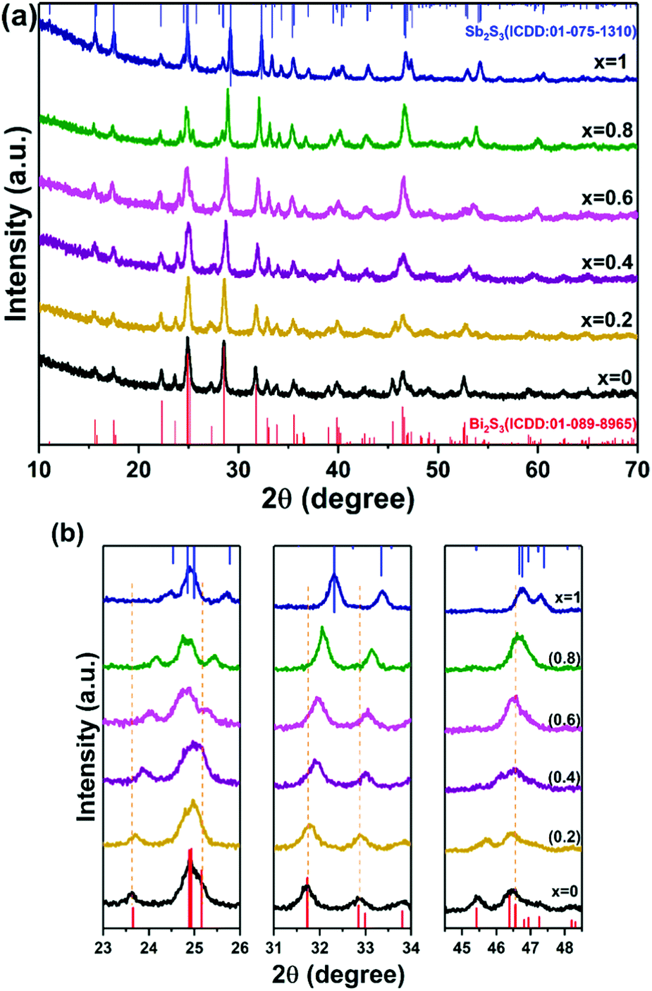 | ||
| Fig. 2 (a) XRD patterns of Bi2S3, Sb2S3 and Bi2−2xSb2xS3 with variations in Sb/Sb+Bi molar ratios at 250 °C with standard patterns of Bi2S3 (bottom) and Sb2S3 (top). (b) Shows the shift of diffraction peaks to larger values as the composition x changes from 0 to 1. | ||
Table 1 shows the unit cell lattice parameters a, b and c and unit cell volume V for Bi2−2xSb2xS3 (0 ≤ x ≤ 1), which were calculated from the X-ray-diffraction data using the lattice relation for orthorhombic structure; 1/d2 = h2/a2 + k2/b2 + l2/c2 and V = abc, where d is lattice plane spacing and (hkl) are the Miller indices of the plane.69 The lattice parameters of Bi2S3 and Sb2S3 were in agreement with literature values (ICDD: 01-089-8965 for Bi2S3 and ICDD: 01-075-1310 for Sb2S3).67,68 Lattice parameters are plotted against the variations in Sb/Sb+Bi molar ratios (Fig. 4). It is clearly seen that a and b increase linearly as the mole fraction of Sb increases, whereas c and V decrease gradually with an increase in the Sb content. A decrease of almost 3.5% in the volume was observed as moving from Bi2S3 to Sb2S3. This is in accordance with the smaller atomic radius of antimony compared to bismuth and with literature X-ray data for Bi2−xSbxS3 films prepared by the dip-dry method.70
| x | Composition | Lattice parameters | EDX (at%) | E g (eV) | |||||
|---|---|---|---|---|---|---|---|---|---|
| a (Å) | b (Å) | c (Å) | V (Å3) | Bi | Sb | S | |||
| 0 | Bi2S3 | 11.173 ± 0.00078 | 11.322 ± 0.00079 | 3.989 ± 0.00028 | 504.61 ± 0.062 | 43 ± 2.1 | 0 | 56 ± 2.8 | 1.66 |
| 0.2 | Bi1.6Sb0.4S3 | 11.185 ± 0.00078 | 11.324 ± 0.00079 | 3.981 ± 0.00028 | 504.23 ± 0.061 | 37 ± 1.8 | 11 ± 0.5 | 52 ± 2.6 | 1.72 |
| 0.4 | Bi1.2Sb0.8S3 | 11.209 ± 0.00078 | 11.325 ± 0.00079 | 3.936 ± 0.00028 | 499.64 ± 0.060 | 28 ± 1.3 | 18 ± 0.8 | 55 ± 2.7 | 1.75 |
| 0.6 | Bi0.8Sb1.2S3 | 11.233 ± 0.00077 | 11.328 ± 0.00078 | 3.878 ± 0.00027 | 493.46 ± 0.059 | 17 ± 0.8 | 27 ± 1.3 | 56 ± 2.8 | 1.88 |
| 0.8 | Bi0.4Sb1.6S3 | 11.245 ± 0.00077 | 11.332 ± 0.00078 | 3.855 ± 0.00027 | 491.24 ± 0.059 | 8 ± 0.4 | 33 ± 1.6 | 59 ± 2.9 | 2.08 |
| 1 | Sb2S3 | 11.248 ± 0.00076 | 11.334 ± 0.00078 | 3.829 ± 0.00026 | 488.14 ± 0.058 | 0 | 41 ± 2.0 | 59 ± 2.9 | 2.19 |
 | ||
| Fig. 3 Comparison of change in Sb content found in elemental analysis of Bi2−2xSb2xS3 (0 ≤ x ≤ 1) with increasing antimony molar ratio by EDX and ICP. The inset shows the plots of ICP versus EDX. | ||
The substitution of Sb3+ for Bi3+ ions in the Bi–Sb–S solid solution series causes the contraction of the inter-rod distance, which is the main factor for increasing the a and b unit cell parameters from the Bi to the Sb forms.71 For the c unit cell parameter, a continuous contraction is observed in going along the solid solution which may be related to the contraction of rods along this direction as a consequence of the decrease of the M–S bond lengths from Bi2S3 to Sb2S3.71
The elemental compositions of Bi2−2xSb2xS3 (0 ≤ x ≤ 1) samples were examined through EDX and ICP-OES. EDX spectra (ESI,† Fig. S3) of the Bi–Sb–S alloys show the characteristic peaks of bismuth Mα, antimony Lα, and sulfur Kα. Table 1 shows the atomic percentages of bismuth, antimony, and sulfur for all compositions calculated by EDX. The analysis was performed for several different areas which all yielded similar results, suggesting a uniform elemental distribution. The results of both EDX and ICP-OES are consistent and confirm that the atomic ratios of all these samples have the expected Sb content in the precursor mixture (Fig. 3). All samples were found to be slightly sulfur deficient (Table 1), perhaps due to the high partial pressure of the sulfur, which causes the evaporation of sulfur at high temperature.72
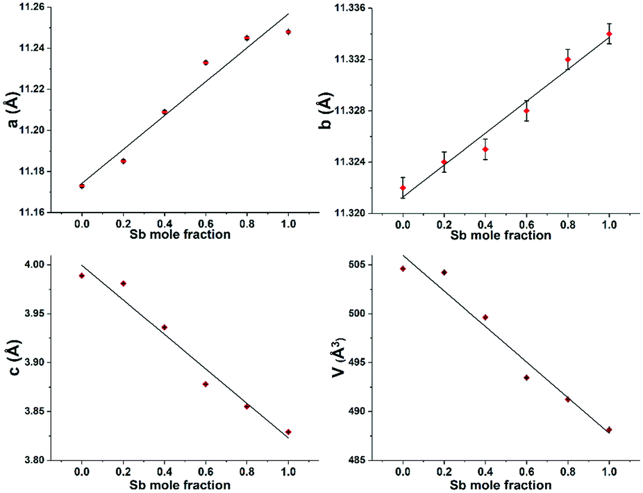 | ||
| Fig. 4 Lattice parameters a, b, c and unit cell volume V of Bi2−2xSb2xS3 (0 ≤ x ≤ 1) with the different mole fractions of antimony. | ||
Raman spectroscopy was used to investigate the Bi2−2xSb2xS3 (0 ≤ x ≤ 1) samples prepared from mixtures of bismuth and antimony xanthates at 250 °C (Fig. 5). The pure Bi2S3 sample shows a weak peak at 184 cm−1 and other two dominant peaks located at 235 and 255.4 cm−1, which is in agreement with the Raman analysis reported for Bi2S3.53,59,73 The low intensity peak at 184 cm−1 is assigned to the Ag symmetric bending modes, and the peaks at 235 and 255 cm−1 are assigned to the Ag and B1g anti-symmetric stretching modes, respectively.59,74 Similarly, the Raman spectrum of the pure Sb2S3 indicates peaks at 186, 250, 280, 301 and 448 cm−1 corresponding to the Raman spectrum of orthorhombic Sb2S3.75–79 It is proposed to assign the peak at 186 cm−1 to the B1g anti-symmetric S–Sb–S bending modes, the peak at 250 cm−1 to the Ag symmetric S–Sb–S bending modes, and the peaks at 280 and 301 cm−1 to the Ag and B1g anti-symmetric Sb–S stretching modes, respectively.74,77 For the Bi2−2xSb2xS3 (x = 0.2, 0.4, 0.6 and 0.8), the Ag and B1g modes, which involve the vibration of metal and sulfur atoms are shifted continuously toward higher wavenumbers with increasing antimony content. The large shift of corresponding peaks to higher wavenumbers in Sb2S3 is caused by both the lower mass of Sb and the shorter Sb–S distances in comparison with Bi–S.74
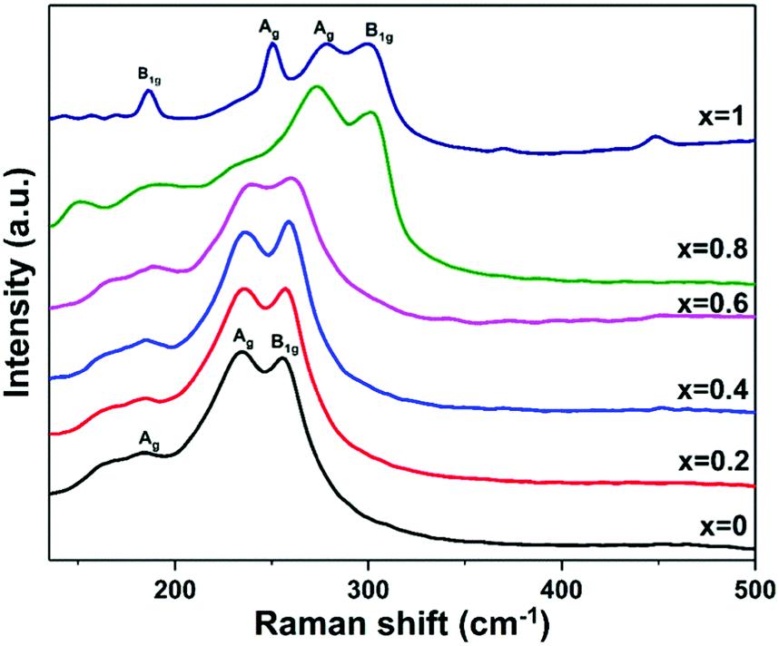 | ||
| Fig. 5 Raman spectra of Bi2−2xSb2xS3 (0 ≤ x ≤ 1) samples prepared by melt thermolysis at 250 °C using bismuth and antimony xanthate precursors with different mole fractions of Sb. | ||
The morphology of all the samples was observed using SEM. Images of Bi2−2xSb2xS3 obtained at 250 °C using 0, 0.2, 0.4, 0.6, 0.8 and 1 mole fractions of Sb are presented in Fig. 6. The SEM image of pure Bi2S3 (x = 0) revealed nanorod structures (Fig. 6a), which changed to slightly thicker nanorods as the Sb content increased to 0.4 mole fraction (Fig. 6b and c). The samples with higher mole fractions of Sb showed completely different morphologies; large particles were observed on addition of 0.6 and 0.8 mole fractions of Sb, which themselves consist of nano-sized rods (Fig. 6d and e). Finally, the SEM image of pure Sb2S3 (x = 1) revealed uneven particles (Fig. 6f). EDX spectrum mapping of the mixed samples prepared at all the compositions x are shown in Fig. 7. It is clearly seen that at this length scale all the elements (Bi, Sb and S) were evenly distributed throughout the entire sample.
 | ||
| Fig. 6 SEM representative secondary electron SEM images (10 kV) of Bi2−2xSb2xS3 (0 ≤ x ≤ 1) samples prepared by melt thermolysis at 250 °C using bismuth and antimony xanthate precursors with different mole fractions of antimony: (a) x = 0 (Bi2S3), (b) x = 0.2, (c) x = 0.4, (d) x = 0.6, (e) x = 0.8 and (f) x = 1 (Sb2S3). Insets: SEM images of samples at higher magnification. | ||
 | ||
| Fig. 7 EDX elemental mapping (20 kV) of Bi Mα, Sb Lα and S Kα for Bi2−2xSb2xS3 samples. (a) x = 0.2, (b) x = 0.4, (c) x = 0.6 and (d) x = 0.8 mole fractions of antimony. | ||
TEM electron diffraction (ED) was used to characterise the local Bi2−2xSb2xS3 crystal structure for two samples (x = 0.2, 0.8). The Bi2−2xSb2xS3 was ground to a fine powder and placed on a holey carbon grid. As with SEM, significant differences in morphology were observed for each sample: for x = 0.2 crystalline nanorods were observed, while for x = 0.8 the material was in the form of bulky, clustered particles (Fig. S6, ESI†). Fig. 8a shows electron diffraction patterns for each sample with ‘spotty’ rings characteristic of many randomly orientated crystals being present within the sample region chosen by the selected area aperture. The presence of many small crystallites is confirmed by TEM imaging (Fig. 8b and Fig. S6, ESI†). The radii of the coloured arcs overlaid on the ED patterns in Fig. 8a correspond to the (hkl) lattice spacings determined from p-XRD data. Table S3 (ESI†) compares the lattice spacings measured by radial averaging of the ED data with the expected interplanar spacings predicted from the bulk p-XRD analysis (Table 1). These show a good match within the measurement accuracy of the ED data.
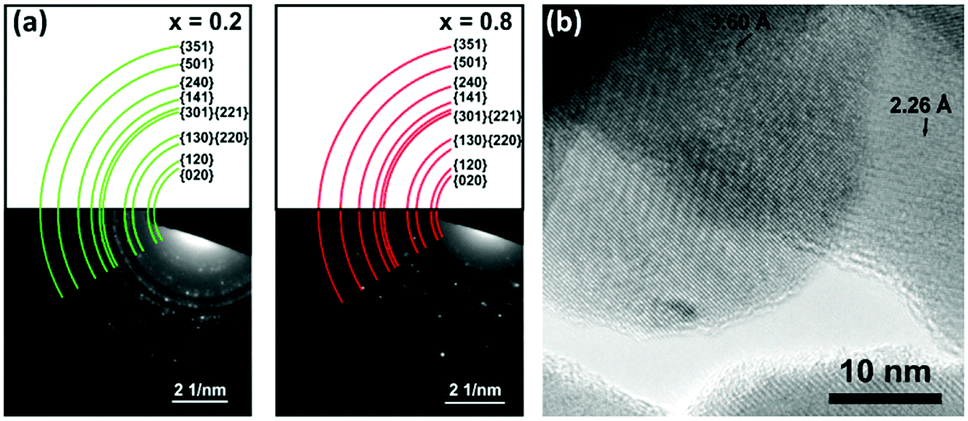 | ||
| Fig. 8 (a) Electron diffraction patterns of Bi2−2xSb2xS3 for x = 0.2 (left) and x = 0.8 (right). Coloured rings represent d-spacings for x = 0.2 (left) and x = 0.8 (right) identified by p-XRD. The ED data also contains additional lattice spacings for the crystal structure which are indexed in Table S3 (ESI†). The presence of additional lattice spacings in the ED data is expected as the ED condition for constructive interference is less severe than for p-XRD (due to the small electron wavelength and small size of the crystallites). (b) TEM micrograph showing several individual crystallites for Bi2−2xSb2xS3, x = 0.8. Lattice spacings of 2.2 Å and 3.6 Å were assigned to the (141) and (130) planes, respectively. | ||
For optical bandgap measurements, thin-film samples of Bi2−2xSb2xS3 were prepared by spin coating different molar concentrations of precursors (1):(2) on glass substrate to yield mole fractions x = 0, 0.2, 0.4, 0.6, 0.8 and 1, and then annealed in quartz tube under nitrogen at 250 °C for an hour. Optical absorption spectra of these samples have been recorded in wavelength range of 400–1000 nm (Fig. S7, ESI†). The band gap of the films can be calculated using the formula (αhν)n = A(hν − Eg), where Eg is the optical band gap, hν is the photon energy, α is the absorption coefficient, A is a constant characteristic of the material, and n = 2, 1/2 for allowed direct and allowed indirect transitions, respectively. Bi2S3 and Sb2S3 are direct band gap materials.80,81 Plots of the (αhν)nversus hν for n = 2 and 1/2 show a linear behaviour for n = 2, which confirms the presence of a direct transition in the Bi2−2xSb2xS3 samples for all compositions (Fig. S8, ESI†). Fig. S8, ESI† presents a Tauc plot to determine the band gaps for all Bi2−2xSb2xS3 samples. For the binary Bi2S3 and Sb2S3 compositions, the direct band gaps were found to be 1.66 and 2.19 eV, respectively; very close to the reported values for these materials.3,35,80–83 The values of the band gap for the mixed samples Bi2−2xSb2xS3 were estimated to be 1.72, 1.75, 1.88 and 2.08 eV for x = 0.2, 0.4, 0.6 and 0.8, respectively, values which lie between those of pure Bi2S3 and Sb2S3 (Table 1). Fig. 9 represents the dependence of band gap of the Bi2−2xSb2xS3 samples on composition, demonstrating that the band gap of Bi2−2xSb2xS3 films increases from 1.66 to 2.19 eV with increasing Sb concentration. This gradual change in the band gap confirms the formation of solid solution. A deviation from a linear trend is probably due to the slight stoichiometric variations in the synthesized solid solution.84 Similar observations for (Bi1−x,Sbx)2S3 thin films grown by arrested precipitation and spray pyrolysis techniques have been reported.66,85 Patil et al. found that the films have a band gap of 1.8 eV for Bi2S3 and 2.3 eV for Sb2S3, whereas the mixed films have band gaps in the range of 1.85–2.27 eV with increasing Sb content in the films.66 It has also been found that incorporation of only 3% bismuth into Sb2S3 narrowed the band gap from 1.72 to 1.59 eV.86
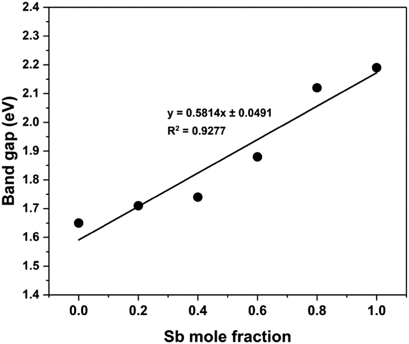 | ||
| Fig. 9 Variation of the band gap for Bi2−2xSb2xS3 (0 ≤ x ≤ 1) samples as a function of mole fraction (x) of antimony. | ||
Conclusions
Bi2−2xSb2xS3 (0 ≤ x ≤ 1) solid solution, with controllable compositions were successfully synthesized via solventless thermolysis using molecular precursors. Structural analysis via p-XRD and TEM-ED indicates the successful incorporation of antimony as a solid solution into the parent bismuth sulfide. SEM images showed changes in the morphology as the amount of antimony was increased in the samples. The elemental compositions of all the samples were examined via ICP-OES and EDX spectroscopic mapping, with the latter technique revealing uniform spatial distribution of elements in all samples. The band gaps of Bi2−2xSb2xS3 films were found to vary from 1.66 eV for Bi2S3 to 2.19 eV for Sb2S3 with increasing antimony mole fraction (x). These ternary bismuth–antimony chalcogenides may find applications as photoelectrocatalysts for solar water splitting,87 as their band gap lies within the suitable range for such applications. The approach provides a simple, scalable and efficient synthesis route to produce ternary sulfide materials with electronic properties that are tuneable across the full compositional range, which, given the rich range of metal xanthate precursors available, gives an exciting opportunity for the low temperature synthesis of a range of semiconductors.Conflicts of interest
There are no conflicts of interest to declare.Acknowledgements
T. A. thanks the Imam Abdulrahman Bin Faisal University for the funding support and for allowing a period of study in the U.K., and also, the Saudi Arabian Cultural Bureau in London for their assistance and support. S. J. H. and D. J. K. thank the Engineering and Physical Sciences (EPSRC) U.K (grants EP/P009050/1 and the NowNANO Graphene CDT), the Defense Threat Reduction Agency (HDTRA1-12-1-0013) and the European Research Council (ERC) under the European Union's Horizon 2020 research and innovation program (ERC-2016-STG-EvoluTEM-715502) for funding.Notes and references
- J. J. Carey, J. P. Allen, D. O. Scanlon and G. W. Watson, J. Solid State Chem., 2014, 213, 116–125 CrossRef CAS.
- O. Savadogo and K. C. Mandal, Sol. Energy Mater. Sol. Cells, 1992, 26, 117–136 CrossRef CAS.
- S. H. Pawar, P. N. Bhosale, M. D. Uplane and S. Tamhankar, Thin Solid Films, 1983, 110, 165–170 CrossRef CAS.
- D. Arivuoli, F. D. Gnanam and P. Ramasamy, J. Mater. Sci. Lett., 1988, 7, 711–713 CrossRef CAS.
- R. Suarez, P. K. Nair and P. V. Kamat, Langmuir, 1998, 14, 3236–3241 CrossRef CAS.
- Y. Luo, J. Yang, Q. Jiang, L. Fu, Y. Xiao, W. Li, D. Zhang, Z. Zhou and Y. Cheng, Nano Energy, 2015, 15, 709–718 CrossRef CAS.
- L. P. Hu, T. J. Zhu, X. Q. Yue, X. H. Liu, Y. G. Wang, Z. J. Xu and X. B. Zhao, Acta Mater., 2015, 85, 270–278 CrossRef CAS.
- J. H. Sung, H. Heo, I. Hwang, M. Lim, D. Lee, K. Kang, H. C. Choi, J.-H. Park, S.-H. Jhi and M.-H. Jo, Nano Lett., 2014, 14, 4030–4035 CrossRef CAS PubMed.
- W. Liu, C. F. Guo, M. Yao, Y. Lan, H. Zhang, Q. Zhang, S. Chen, C. P. Opeil and Z. Ren, Nano Energy, 2014, 4, 113–122 CrossRef CAS.
- S.-C. Liufu, L.-D. Chen, Q. Yao and C.-F. Wang, Appl. Phys. Lett., 2007, 90, 112106 CrossRef.
- S. Messina, M. T. S. Nair and P. K. Nair, Thin Solid Films, 2007, 515, 5777–5782 CrossRef CAS.
- J. George and M. K. Radhakrishnan, Solid State Commun., 1980, 33, 987–989 CrossRef CAS.
- R. S. Mane, B. R. Sankapal and C. D. Lokhande, Mater. Chem. Phys., 1999, 60, 158–162 CrossRef CAS.
- A. K. Rath, M. Bernechea, L. Martinez and G. Konstantatos, Adv. Mater., 2011, 23, 3712–3717 CrossRef CAS PubMed.
- G.-Y. Liu, L.-Y. Xu, F. Zhou, Y. Zhang, H. Li, Q. F. Xu and J. M. Lu, Phys. Chem. Chem. Phys., 2013, 15, 11554–11558 RSC.
- Z. Wang, S. Qu, X. Zeng, J. Liu, F. Tan, L. Jin and Z. Wang, Appl. Surf. Sci., 2010, 257, 423–428 CrossRef CAS.
- Y. Y. Wang, K. F. Cai and X. Yao, J. Nanopart. Res., 2012, 14, 848 CrossRef.
- G. Springer and J. Laflamme, Can. Mineral., 1971, 10, 847–853 CAS.
- G. Springer, Mineral. Mag., 1969, 37, 294–296 CrossRef CAS.
- V. W. Lueth, P. C. Goodell and N. E. Pingitore, Econ. Geol., 1990, 85, 1462–1472 CrossRef CAS.
- S. Ghosal and R. Sack, Mineral. Mag., 1999, 63, 723–733 CrossRef CAS.
- A. Kyono and M. Kimata, Am. Mineral., 2004, 89, 932–940 CrossRef CAS.
- H. Hu, M. Mo, B. Yang, X. Zhang, Q. Li, W. Yu and Y. Qian, J. Cryst. Growth, 2003, 258, 106–112 CrossRef CAS.
- X.-Y. Ma, L. Liu, W.-L. Mo, H. Liu, H.-Z. Kou and Y. Wang, J. Cryst. Growth, 2007, 306, 159–165 CrossRef CAS.
- J. Wang and Y. Li, Mater. Chem. Phys., 2004, 87, 420–423 CrossRef CAS.
- J. Lu, Q. Han, X. Yang, L. Lu and X. Wang, Mater. Lett., 2007, 61, 3425–3428 CrossRef CAS.
- J. R. Castro, K. C. Molloy, Y. Liu, C. S. Lai, Z. Dong, T. J. White and E. R. T. Tiekink, J. Mater. Chem., 2008, 18, 5399–5405 RSC.
- L. Tian, H. Yao Tan and J. J. Vittal, Cryst. Growth Des., 2008, 8, 734–738 CrossRef.
- G. Murtaza, M. Akhtar, M. Azad Malik, P. O’Brien and N. Revaprasadu, Mater. Sci. Semicond. Process., 2015, 40, 643–649 CrossRef CAS.
- O. C. Monteiro, T. Trindade, J. H. Park and P. O'Brien, Chem. Vap. Deposition, 2000, 6, 230–232 CrossRef CAS.
- M. Abulikemu, S. Del Gobbo, D. H. Anjum, M. A. Malik and O. M. Bakr, J. Mater. Chem. A, 2016, 4, 6809–6814 RSC.
- P. Christian and P. O'Brien, J. Mater. Chem., 2005, 15, 4949–4954 RSC.
- M. B. Sigman and B. A. Korgel, Chem. Mater., 2005, 17, 1655–1660 CrossRef CAS.
- B. B. Nayak, H. N. Acharya, T. K. Chaudhuri and G. B. Mitra, Thin Solid Films, 1982, 92, 309–314 CrossRef CAS.
- R. S. Mane and C. D. Lokhande, Mater. Chem. Phys., 2003, 82, 347–354 CrossRef CAS.
- A. U. Ubale, Mater. Chem. Phys., 2010, 121, 555–560 CrossRef CAS.
- J. Rodriguez-Castro, M. F. Mahon and K. C. Molloy, Chem. Vap. Deposition, 2006, 12, 601–607 CrossRef CAS.
- S. R. Gadakh and C. H. Bhosale, Mater. Chem. Phys., 2003, 78, 367–371 CrossRef CAS.
- M. Madoun, R. Baghdad, K. Chebbah, M. A. Bezzerrouk, L. Michez and N. Benramdane, Mater. Sci. Semicond. Process., 2013, 16, 2084–2090 CrossRef CAS.
- B. R. Sankapal, R. S. Mane and C. D. Lokhande, J. Mater. Sci. Lett., 1999, 18, 1453–1455 CrossRef CAS.
- A. U. Ubale, A. S. Daryapurkar, R. B. Mankar, R. R. Raut, V. S. Sangawar and C. H. Bhosale, Mater. Chem. Phys., 2008, 110, 180–185 CrossRef CAS.
- T. H. Larsen, M. Sigman, A. Ghezelbash, R. C. Doty and B. A. Korgel, J. Am. Chem. Soc., 2003, 125, 5638–5639 CrossRef CAS PubMed.
- J. Chen, L. Chen and L.-M. Wu, Inorg. Chem., 2007, 46, 8038–8043 CrossRef CAS PubMed.
- K. Abe, T. Hanada, Y. Yoshida, N. Tanigaki, H. Takiguchi, H. Nagasawa, M. Nakamoto, T. Yamaguchi and K. Yase, Thin Solid Films, 1998, 327-329, 524–527 CrossRef CAS.
- Y.-B. Chen, L. Chen and L.-M. Wu, Inorg. Chem., 2005, 44, 9817–9822 CrossRef CAS PubMed.
- E. Lewis, S. Haigh and P. O'Brien, J. Mater. Chem. A, 2014, 2, 570–580 RSC.
- N. L. Pickett and P. O’Brien, Chem. Rec., 2001, 1, 467–479 CrossRef CAS PubMed.
- G. Xie, Z.-P. Qiao, M.-H. Zeng, X.-M. Chen and S.-L. Gao, Cryst. Growth Des., 2004, 4, 513–516 CrossRef CAS.
- A. Tang, Q. Yang and Y. Qian, Inorg. Chem., 2003, 42, 8081–8086 CrossRef PubMed.
- O. C. Monteiro and T. Trindade, J. Mater. Sci. Lett., 2000, 19, 859–861 CrossRef CAS.
- O. C. Monteiro, H. I. S. Nogueira, T. Trindade and M. Motevalli, Chem. Mater., 2001, 13, 2103–2111 CrossRef CAS.
- M. Lazell, S. J. Nørager, P. O'Brien and N. Revaprasadu, Mater. Sci. Eng., C, 2001, 16, 129–133 CrossRef.
- X.-P. Shen, G. Yin, W.-L. Zhang and Z. Xu, Solid State Commun., 2006, 140, 116–119 CrossRef CAS.
- W. Lou, M. Chen, X. Wang and W. Liu, Chem. Mater., 2007, 19, 872–878 CrossRef CAS.
- J. Yang, J.-h. Zeng, S.-H. Yu, L. Yang, Y.-H. Zhang and Y.-T. Qian, Chem. Mater., 2000, 12, 2924–2929 CrossRef CAS.
- V. Stavila, K. H. Whitmire and I. Rusakova, Chem. Mater., 2009, 21, 5456–5465 CrossRef CAS.
- N. Bansal, F. T. F. O'Mahony, T. Lutz and S. A. Haque, Adv. Energy Mater., 2013, 3, 986–990 CrossRef CAS.
- Q. Han, L. Chen, M. Wang, X. Yang, L. Lu and X. Wang, Mater. Sci. Eng., B, 2010, 166, 118–121 CrossRef CAS.
- V. Kaltenhauser, T. Rath, W. Haas, A. Torvisco, S. K. Muller, B. Friedel, B. Kunert, R. Saf, F. Hofer and G. Trimmel, J. Mater. Chem. C, 2013, 1, 7825–7832 RSC.
- A. Gupta, R. K. Sharma, R. Bohra, V. K. Jain, J. E. Drake, M. B. Hursthouse and M. E. Light, J. Organomet. Chem., 2003, 678, 122–127 CrossRef CAS.
- Y. W. Koh, C. S. Lai, A. Y. Du, E. R. T. Tiekink and K. P. Loh, Chem. Mater., 2003, 15, 4544–4554 CrossRef CAS.
- E. Tavasoli, Y. Guo, P. Kunal, J. Grajeda, A. Gerber and J. Vela, Chem. Mater., 2012, 24, 4231–4241 CrossRef CAS.
- Y. C. Li, M. F. Ye, C. H. Yang, X. H. Li and Y. F. Li, Adv. Funct. Mater., 2005, 15, 433–441 CrossRef CAS.
- N. Pradhan, B. Katz and S. Efrima, J. Phys. Chem. B, 2003, 107, 13843–13854 CrossRef CAS.
- J. Sun, X. Shen, L. Guo, G. Wang, J. Park and K. Wang, Nanoscale Res. Lett., 2009, 5, 364 CrossRef PubMed.
- V. A. Patil, A. R. Patil, J. W. Choi, D. S. Paik and S. J. Yoon, Surf. Eng., 2007, 23, 28–31 CrossRef CAS.
- K. Łukaszewicz, J. Stępień-Damm, A. Pietraszko, A. Kajokas and J. Grigas, Pol. J. Chem., 1999, 73, 541–546 Search PubMed.
- S. Šćavničar, Z. Kristallogr. - Cryst. Mater., 1960, 114, 85–97 CrossRef.
- B. D. Cullity and S. R. Stock, Elements of X-ray Diffraction, Pearson Education, 2014 Search PubMed.
- B. B. Nayak, H. N. Acharya, G. B. Mitra and B. K. Mathur, Thin Solid Films, 1983, 105, 17–24 CrossRef CAS.
- D. Poleti, L. Karanović, T. Balić-Žunić and I. Gržetić, Neues Jahrb. Mineral., 2012, 189, 177–187 CAS.
- M. Al-Shakban, Z. Xie, N. Savjani, M. A. Malik and P. O’Brien, J. Mater. Sci., 2016, 51, 6166–6172 CrossRef CAS.
- Y. Zhao, K. T. E. Chua, C. K. Gan, J. Zhang, B. Peng, Z. Peng and Q. Xiong, Phys. Rev. B: Condens. Matter Mater. Phys., 2011, 84, 205330 CrossRef.
- S. Kharbish, E. Libowitzky and A. Beran, Eur. J. Mineral., 2009, 21, 325–333 CrossRef CAS.
- S. Shaji, L. V. Garcia, S. L. Loredo, B. Krishnan, J. A. Aguilar Martinez, T. K. Das Roy and D. A. Avellaneda, Appl. Surf. Sci., 2017, 393, 369–376 CrossRef CAS.
- R. G. Avilez Garcia, C. A. Meza Avendaño, M. Pal, F. Paraguay Delgado and N. R. Mathews, Mater. Sci. Semicond. Process., 2016, 44, 91–100 CrossRef CAS.
- M. Medles, N. Benramdane, A. Bouzidi, K. Sahraoui, R. Miloua, R. Desfeux and C. Mathieu, J. Optoelectron. Adv. Mater., 2014, 16, 726–731 CAS.
- G. Wang and C. L. Cheung, Mater. Lett., 2012, 67, 222–225 CrossRef CAS.
- J. Ota, P. Roy, S. K. Srivastava, B. B. Nayak and A. K. Saxena, Cryst. Growth Des., 2008, 8, 2019–2023 CrossRef CAS.
- M. Y. Versavel and J. A. Haber, Thin Solid Films, 2007, 515, 7171–7176 CrossRef CAS.
- C. D. Lokhande, A. U. Ubale and P. S. Patil, Thin Solid Films, 1997, 302, 1–4 CrossRef CAS.
- Q. Han, J. Chen, X. Yang, L. Lu and X. Wang, J. Phys. Chem. C, 2007, 111, 14072–14077 CrossRef CAS.
- A. M. Salem, M. S. Selim and A. M. Salem, J. Phys. D: Appl. Phys., 2001, 34, 12 CrossRef CAS.
- F. Vines, G. Konstantatos and F. Illas, Phys. Chem. Chem. Phys., 2017, 19, 27940–27944 RSC.
- P. Usha Rajalakshmi, R. Oommen, C. Sanjeeviraja and V. Ganesan, Superlattices Microstruct., 2013, 57, 158–165 CrossRef CAS.
- S. Ito, K. Tsujimoto, D.-C. Nguyen, K. Manabe and H. Nishino, Int. J. Hydrogen Energy, 2013, 38, 16749–16754 CrossRef CAS.
- B. K. Patra, S. Khilari, A. Bera, S. K. Mehetor, D. Pradhan and N. Pradhan, Chem. Mater., 2017, 29, 1116–1126 CrossRef CAS.
Footnote |
| † Electronic supplementary information (ESI) available: p-XRD patterns of Bi2S3 and Sb2S3 materials and absorption spectra of Bi2−2xSb2xS3. See DOI: 10.1039/c8tc02374c |
| This journal is © The Royal Society of Chemistry 2018 |