
 Open Access Article
 This Open Access Article is licensed under a Creative Commons Attribution-Non Commercial 3.0 Unported Licence
Cu2O@PNIPAM core–shell microgels as novel inkjet materials for the preparation of CuO hollow porous nanocubes gas sensing layers†
He
Jia
a,
Haitao
Gao
b,
Shilin
Mei
a,
Janosch
Kneer
b,
Xianzhong
Lin
c,
Qidi
Ran
 a,
Fuxian
Wang
d,
Stefan
Palzer
e and
Yan
Lu
*af
a,
Fuxian
Wang
d,
Stefan
Palzer
e and
Yan
Lu
*af
aSoft Matter and Functional Materials, Helmholtz-Zentrum Berlin für Materialien und Energie, Hahn-Meitner-Platz 1, Berlin, Germany. E-mail: yan.lu@helmholtz-berlin.de
bLaboratory for Gas Sensors, Department of Microsystems Engineering – IMTEK, University of Freiburg, Georges-Köhler-Allee 102, Freiburg, Germany
cHeterogeneous Materialien und Energie, Helmholtz-Zentrum Berlin für Materialien und Energie, Hahn-Meitner-Platz 1, Berlin, Germany
dInstitute for Solar Fuels, Helmholtz-Zentrum Berlin für Materialien und Energie GmbH, 14109 Berlin, Germany
eDepartment of Computer Science, Universidad Autónoma de Madrid, Francisco Tomás y Valiente 11, 28049 Madrid, Spain
fInstitute of Chemistry, University of Potsdam, 14467 Potsdam, Germany
First published on 18th June 2018
Abstract
There has been long-standing interest in developing metal oxide-based sensors with high sensitivity, selectivity, fast response and low material consumption. Here we report for the first time the utilization of Cu2O@PNIPAM core–shell microgels with a nanocube-shaped core structure for construction of novel CuO gas sensing layers. The hybrid microgels show significant improvement in colloidal stability as compared to native Cu2O nanocubes. Consequently, a homogeneous thin film of Cu2O@PNIPAM nanoparticles can be engineered in a quite low solid content (1.5 wt%) by inkjet printing of the dispersion at an optimized viscosity and surface tension. Most importantly, thermal treatment of the Cu2O@PNIPAM microgels forms porous CuO nanocubes, which show much faster response to relevant trace NO2 gases than sensors produced from bare Cu2O nanocubes. This outcome is due to the fact that the PNIPAM shell can successfully hinder the aggregation of CuO nanoparticles during pyrolysis, which enables full utilization of the sensor layers and better access of the gas to active sites. These results point out great potential of such an innovative system as gas sensors with low cost, fast response and high sensitivity.
Introduction
Semiconducting metal oxide-based gas sensors currently constitute one of the most investigated gas detection technologies due to their low cost, low power consumption, simple construction, and a broad range of detectable gases.1–4 With the aim of enhancing sensitivity, selectivity, and response time, numerous efforts have been made to synthesize metal oxide nanostructures with high porosity, large surface area and a rich number of active sites.5,6 In addition to the emphasis on morphology, the preservation of the defined nanostructures against transformation or deformation during manufacture have also attracted remarkable attention, which is essential to fully utilize the sensing layers and minimize the cost. However, achieving co-benefits of less material consumption, fast response, and higher sensitivity and selectivity has been an enduring challenge due to much less focus on the stabilization of semiconducting metal oxide nanoparticles, which is particularly important for the application of environmentally sensitive metal oxides such as Cu2O.Cu2O is a well-known p-type semiconductor, which has been widely applied in photocatalytic degradation of dye molecules,7–9 solar energy conversion,10 lithium-ion batteries11,12 and gas sensors.13,14 It can be also used as precursor particles for fabricating CuO materials.15 Due to the possibility to achieve highly selective detection of the toxic gas using Cu2O and CuO as sensing material, both Cu2O and CuO are of great interest in material research.16–18 Consequently, the deposition of Cu2O nanoparticles onto various substrates is of great importance in the construction of gas sensors, which has significant impact on the performance of the sensing layers.19,20 Among the plethora of possible deposition techniques for nanostructures,21 inkjet printing stands out as a flexible and scalable backend production process of functional layers. Inkjet printing has been one of the most effective deposition techniques due to its numerous advantages, such as economic use of functional materials, superior control of film thickness in nano-/micro-scale, and its feasibility to fabricate high quality patterns onto both hard and flexible substrates in a large volume production as well as in small batches.22 Moreover, a combination of inkjet printing technology with so-called hotplate devices allows for quickly testing novel nano-sized gas sensitive materials.15,23–25
The strict requirements for the properties of the ink system top the list of challenges needed to be overcome for inkjet printing of Cu2O nanoparticles. On the one hand, the stability of the ink system should meet the requirement to attain monodispersed patterns on the substrates without aggregation and can be long-term stored without deterioration. On the other hand, in order to obtain high resolution of the printed patterns, the viscosity and surface tension of the ink should be beneficial to minimize the size of the droplets according to Fromm's theory developed in 1984.26,27,42
Unfortunately, Cu2O nanoparticles typically exhibit low environmental stability in water and the nanostructures are easily destroyed in an oxidation process. Thus, currently it remains hard to prepare inks with Cu2O nanoparticles to meet all of the above requirements. Kim et al.28 and Lee et al.29 tried to stabilize Cu2O nanoparticles in an aqueous solvent mixed with isopropanol or glycerol respectively, to improve the viscosity and surface tension of the ink. But the stability of Cu2O individuals did not change significantly. Dasgupta et al.30 chose sodium salt of poly(acrylic acid) (PAANa) as the stabilizer to prevent the oxidation of Cu2O nanoparticles ink solution. Due to the adsorption of PAANa ligands, the surface energy of the nanoparticles was reduced resulting in a reduced tendency for agglomeration. Yang et al.31 used oleic acid to stabilize Cu2O nanoparticles and dispersed the samples into non-polar solvent instead of water to slow down the process of oxidation. In spite of these efforts, these reported methods can only extend the shelf life of the Cu2O ink solution to a couple of weeks. Although efforts have been continuously made to improve the properties of Cu2O nanoparticle ink solution, there is no effective method to be presented until now.
As one of the most well-known thermosensitive microgels, poly(N-isopropylacrylamide) (PNIPAM) has been used to modify different kinds of inorganic nanoparticles. Due to the hydrophilic property below the lower critical solution temperature (LCST), PNIPAM shells can increase the colloidal stability of nanoparticles in aqueous solution and help form an array with distance between each of the hybrid nanoparticles when they are dried on different substrates.32–38 For instance, Liz-Marzán et al.39 and Karg et al.40 successfully synthesized hybrid systems by encapsulating gold and silver nanoparticles inside PNIPAM shells, respectively. Due to the modification of the PNIPAM shell, the colloidal stability of the nanoparticles was improved and the monolayer arrays of the particles can be obtained. Moreover, after removal of the PNIPAM shells by annealing at 700 °C, a monolayer of well-separated gold nanoparticles can still be retained.40 Recently, we first applied this system to the p-type semiconductors, Cu2O nanocubes. The colloid stability of the Cu2O nanocubes have been enhanced significantly after PNIPAM coating and the PNIPAM shell can protect the Cu2O nanocubes from fast oxidation for several months.41
Here we present for the first time the use of Cu2O@PNIPAM core–shell nanoparticles as a novel ink system for the preparation of gas sensor device by inkjet printing technique. With the protection of the PNIPAM shells, the storage time of Cu2O nanoparticles based ink solution was significantly prolonged, which can be kept for at least 3 months without oxidation. At the same time, the colloidal stability of the ink solution was obviously enhanced. The ink solution remained stable after standing overnight and can easily be redispersed homogeneously before inkjet printing after storing for several months, which guarantees homogeneous deposition. Moreover, Cu2O@PNIPAM aqueous ink solution with low solid content (1.5 wt%) can meet the requirements for obtaining high resolution printed patterns according to Fromm's theory42 without introducing any other surfactant and solvent.
The procedure for the preparation of gas sensor device by inkjet printing with Cu2O@PNIPAM core–shell nanoparticles as the ink material was shown in Scheme 1. Assisted by PNIPAM shells, a homogeneous thin layer of Cu2O@PNIPAM core–shell nanoparticles was obtained, which allows for the construction of multi-layers of Cu2O@PNIPAM devices by repeating the inkjet printing process. Most importantly, after thermal treatment, a gas sensing layer consisting of CuO porous hollow nanocubes was formed and a well-defined space between adjacent CuO nanocubes has been achieved, which significantly increased the specific surface area of the sensing layer and improved the response time of the gas sensor device. The present approach can be easily extended to other functional nanoparticles and it allows for the preparation of gas sensor devices in a more environmentally friendly way by using much less materials. The results obtained with CuO nanocubes here is an addition to the results regarding the shape dependence of both sensitivity and selectivity of gas sensitive layers. The latter is particularly interesting for potential use of layers in real-world applications outside the laboratory, where the response characteristics of various metal-oxide based layers are employed for the so-called electronic noses.43,44
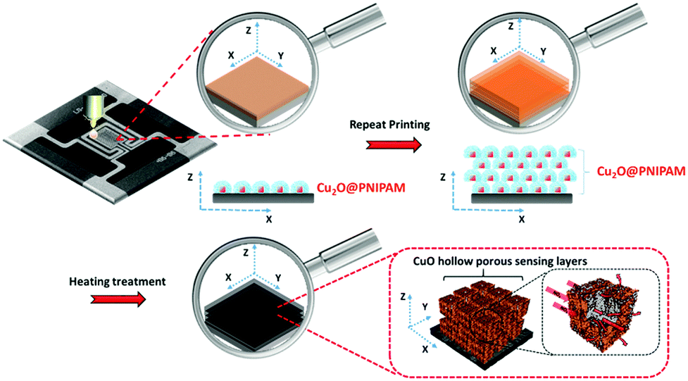 | ||
| Scheme 1 Schematic illustration of the inkjet printing procedure used to fabricate a gas sensor device from Cu2O@PNIPAM core–shell nanoparticles. | ||
Previous results on CuO-based layers include studies of the behavior of microwave-assisted production of urchin-like and fiber-like CuO, as well as nanorods, which had shown the highest response towards NO2 for urchin-like structures and the fastest response for nanorods.45 Previous work has also entailed a comparison of spherical and octahedral CuO15 nanoparticles synthesized via precipitation reaction, porous cages using metal–organic frameworks as templates,46 doped and undoped hollow spheres,47 nanosheets48 and nanoflowers apart from more traditional fabrication methods, such as sputtering.49
Experimental section
Materials and methods
 | ||
| Scheme 2 Schematic illustration of the synthesis procedure of Cu2O@PNIPAM core–shell nanoparticles. | ||
Firstly, Cu2O nanocubes were synthesized by seed-mediated reaction method reported by Michael H. Huang's group50 and washed by centrifugation. In the second step, Cu2O nanocubes (0.66 mg mL−1, 10 mL) were modified with NaSS (0.024 M, 10 mL) and PDDA (0.017 g mL−1, 30 mL) as the interlayer. The unadsorbed PDDA and NaSS molecules can be removed by centrifugation (3500 rpm, 15 min) and the modified Cu2O nanocubes were dispersed into 5 mL H2O. With the help of double bonds supplied by the NaSS, the PNIPAM shells were successfully coated on the surface of Cu2O nanocubes by precipitation polymerization by using V50 (0.018 M, 1 mL) as initiator at 75 °C. The polymerization was started immediately with the addition of 1 mL NIPAM (0.31 M) and BIS (9 mol% of NIPAM) into the mixture solution. The composite particles were then purified by centrifugation for several times and redispersed in water.
 | (1) |
Characterization
The hydrodynamic radius of the samples as a function of temperature was conducted by Zetasizer (Malvern Zetasizer Nano ZS ZEN 3500). Transmission electron microscope (TEM) images were done with JEOL JEM-2100 at 200 kV. X-ray diffraction (XRD) measurements were performed in a Bruker D8 diffractometer in the locked coupled mode (2θ ranging from 10° to 80°) with Cu Kα1 radiation, the incident wavelength is 1.5406 Å. For the accomplished measurements the acceleration voltage is set to 40 kV and the filament current to 40 mA. The amount of Cu2O in the Cu2O@PNIPAM core–shell nanoparticles was determined by thermogravimetric analysis (TGA) using a Netsch STA 409PC LUXX. Fifteen milligrams of dried sample was heated to 800 oC under a constant argon flow (30 mL min−1) with a heating rate of 10 K min−1. Scanning electron microscope (SEM) measurements were done in a SEM LEO GEMINI 1530. Surface-tension was measured at room temperature by Contact Angle System OCA20 from dataphysics using pedant drop configuration. The size distribution of Cu2O nanoparticles was measured using Image J software based on the TEM images. Rheological measurements have been performed with a stress-controlled rheometer (Physica MCR 301, Anton Paar) equipped with cone-plate geometry (CP50). Shear steady tests were done with shear rate increased process from 10−3 to 103 s−1 and the decreased process from 103 to 10−3 s−1. The surface morphology was investigated by atomic force microscope (AFM, Park System, XE – 100) operated in tapping mode using an etched Si tip with a tip radius of 10 nm with force constant of 40 N m−1. All scans were performed on a scale of 40 μm × 40 μm with the lateral resolved height information on a square array of 256 × 256 pixels.Results and discussion
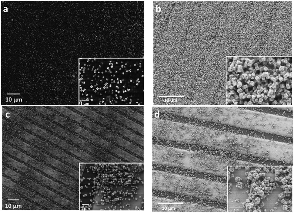
In our previous work,41 we were able to modify Cu2O nanocubes with thermosensitive PNIPAM shells by a two-step approach: the adsorption of an interlayer made up of PDDA and NaSS, and the coating by PNIPAM shells by precipitation polymerization. Due to the strong hydrophilic repulsion below the lower critical solution temperature (LCST) of PNIPAM, the modification of PNIPAM shell can significantly improve the colloidal stability of the Cu2O nanocubes. Fig. 1a shows Cu2O nanocubes without PNIPAM shells, from which aggregations can be clearly observed. Moreover, the photograph in Fig. S2 (ESI†) shows a coffee-ring shaped deposition on the substrate, which is a result of the aggregation of the nanoparticles along the periphery during drying process on a solid surface.26,53 On the contrary, the coffee-ring disappeared after PNIPAM coating and a uniform film consisting of Cu2O@PNIPAM core–shell nanoparticles was obtained, indicating homogeneous deposition of the particles.26,35 | ||
| Fig. 1 SEM images of (a) Cu2O nanocubes, Cu2O@PNIPAM core–shell nanoparticles before (b) and after (c) heating treatment at 350 °C for 1 hour in the air; (d) XRD patterns of the Cu2O@PNIPAM core–shell nanoparticles before (up) and after (below) heating treatment at 350 °C for 1 hour. As reference, standard XRD patterns of CuO (JCPDS: No. 45-0937) and Cu2O (JCPDS: No. 65-3288) are shown in the plot. | ||
As shown in Fig. 1b, the Cu2O@PNIPAM particles spontaneously formed an array of almost constant surface-to-surface distance after drying at room temperature on a Si wafer. The homogeneous deposition is essential to abstain the merging of adjacent particles and is critical to high-resolution inkjet printing patterns. Moreover, the homogeneous patterns and the cubic shapes of the particles were perfectly preserved after annealing at 350 °C under air, where the PNIPAM shell has been completely burned off and the Cu2O nanoparticles have converted into CuO (Fig. 1c and Fig. S3, ESI†). The corresponding X-ray diffraction (XRD) patterns of the Cu2O@PNIPAM core–shell nanoparticles before and after aerobic annealing are presented in Fig. 1d. The original Cu2O signals disappeared completely after the high temperature treatment, while the peaks corresponding to the (110), (002) and (111) planes of CuO emerged according to the JCPDS card (No. 45-0937, red signals in Fig. 1d). This indicates that all of the Cu2O nanoparticles have been transformed to CuO nanoparticles via the heating treatment. Fig. 2 shows the surface topographies of bare Cu2O nanocubes and Cu2O@PNIPAM core–shell nanoparticles on polystyrene (PS) substrate by drop-deposition, respectively. Without the modification of PNIPAM, most of the bare Cu2O nanocubes were aggregated and cannot form a homogeneous thin coating as proved by AFM in Fig. 2a. Thus, parts of the substrate were not covered with nanoparticles. On the contrary, it can be observed from the AFM measurements that the thin film formed by the core–shell nanoparticles possessed much smoother surface and less average grain size than the one formed by the bare Cu2O nanocubes. The root mean square (RMS) roughness obtained by the AFM scanning (40 μm × 40 μm) of the film formed from the core–shell microgels is 84.7 nm. This result further suggests that Cu2O@PNIPAM core–shell nanoparticles can form very homogeneous patterns, which is critical to the high resolution pattern by inkjet printing and may be crucial in obtaining repeatable metal oxide based gas sensor fabrication.19
 | ||
| Fig. 2 AFM images of (a) the bare Cu2O nanocubes and (b) the Cu2O@PNIPAM core–shell nanoparticles drop deposited on PS substrates with the same solid content of 0.026 wt%. | ||
Apart from homogeneous deposition of the particles with patterned distribution and smoother surface, the PNIPAM shells significantly improved the stability of the ink system by forming an extremely stable dispersion. As shown in Fig. S4 (ESI†), the core–shell nanoparticles remained stable in water after storing overnight at room temperature without any visible sediment. Moreover, after being stored for 3 months, the ink solution can be redispersed homogeneously. On the contrary, without PNIPAM coating, an obvious precipitation has been observed for the bare Cu2O nanocubes after 15 min and all of the particles precipitated at the bottom of the bottle overnight. Notably, with the protection of the PNIPAM shells, Cu2O nanocubes can be effectively prevented from oxidation in water-based solutions for several months instead of a couple of weeks at the state of the art level. This property can greatly extend the shelf life of a Cu2O aqueous solution as ink system.
As shown in Fig. 3, after storing in water in a dark place for 90 days, the cubic structure of the bare Cu2O nanoparticles has been completely destroyed due to the oxidation into CuO, which can be also observed from the color change of the solution from orange to black (see the photo inset Fig. 3a and Fig. S4, ESI†). This is emphasized by the observation of new peaks at 2θ = 35.5°, 38.8°, 48.6° and 58.4° corresponding to the Bragg reflections of CuO in the XRD patterns, which indicates the oxidation of bare Cu2O nanocubes (Fig. 3c). In contrast, PNIPAM-modified nanocubes preserved all of the characteristic Cu2O peaks and no other peaks were found in the XRD spectra after storing in water solution under the same condition for 90 days, indicating that none of the Cu2O was oxidized (Fig. 3d). Moreover, all of the Cu2O particles maintained their cubic structure and no aggregation was observed in the system (Fig. 3b).
 | ||
| Fig. 3 SEM images of Cu2O nanocubes without (a) and with (b) PNIPAM coating after 90 days’ storage in aqueous solution; XRD patterns of (c) bare Cu2O nanocubes kept in water at room temperature for 90 days and (d) Cu2O@PNIPAM core–shell nanoparticles with the same treatment. | ||
The physical properties of fluid ink, like viscosity and surface tension, have a close relationship with the printability of the ink system and the resolution of the patterns. This relationship can be represented by the inverse (Z) of the Ohnesorge number as introduced previously. Only when the value of Z is within 1 < Z < 14,26,27 a high resolution pattern can be printed. The relevant physical parameters and corresponding Z values of the bare Cu2O nanocubes and Cu2O@PNIPAM core–shell nanoparticles with different solid content at 20 °C have been listed in Table 1. Due to the more uniform dispersion of the particles in water and the hydrophilicity exhibited by PNIPAM at room temperature, the Cu2O sample with PNIPAM coating presents higher viscosity and lower surface tension than the bare one at the same solid content (1.5 wt%), which leads to a lower Z value in the printable range. While for the bare Cu2O nanocubes, the Z value of the bare Cu2O sample was adjusted within a reasonable range only when the solid content was increased from 1.5 wt% to 8 wt%. Moreover, as shown in Fig. S5 (ESI†), after being kept at room temperature for 30 min, the droplet of the bare Cu2O nanocubes with solid content of 1.5 wt% became inhomogeneous and the upper portion of the droplet began depleted due to sedimentation. The above mentioned three dispersions were used to be printed on the devices (see Fig. S6, ESI†). Without introducing any additives, the device printed from pure Cu2O dispersions with 1.5% solid content could not be uniformly covered by the nanoparticles and most of the device surface was bare. Thus, the Cu2O@PNIPAM core–shell nanoparticle solution with solid content of 1.5 wt% and the pure Cu2O nanocube solution with solid content of 8 wt% were used as the ink to prepare the gas sensor devices.
| Sample | Solid content (wt%) | Viscosity η (mPa s) | Density ρ (g cm−3) | Surface tension γ (mN m−1) | Z (Oh−1) |
|---|---|---|---|---|---|
| Cu2O nanocubes | 1.5 | 1.33 | 1.015 | 69.2 | 22.3 |
| Cu2O @PNIPAM | 1.5 | 1.83 | 1.015 | 42.7 | 12.7 |
| Cu2O nanocubes | 8 | 2.22 | 1.08 | 61 | 12.9 |
The Cu2O@PNIPAM core–shell particles were printed on the interdigitated electrode structures of a micromachined hotplate device, resulting in the gas sensor elements which were subsequently characterized. Before the heating treatment, Cu2O nanocubes were buried inside the PNIPAM shells to form a homogeneous layer (Fig. 4a). After an oxidizing treatment at 350 °C for one hour in the air, the PNIPAM shells were burned off resulting in a uniform layer of CuO nanocubes (Fig. 4b). The inset in Fig. 4b clearly shows that the CuO nanocubes are well separated from each other, no aggregation has been formed after heating treatment. In contrast, big islands of aggregations as well as numerous blank areas can be found on the surface of the device (Fig. 4c). After the oxidization treatment, the cubic structures were totally destroyed by sintering, large yet sparser and random bulky particles were found as shown in the inset of Fig. 4d.
 | ||
| Fig. 4 (a and b) SEM images of gas sensor devices of Cu2O@PNIPAM core–shell nanoparticles before and after heating treatment. (c and d) SEM images of gas sensor device of pure Cu2O nanocubes before and after heating treatment. | ||
Most importantly, the thermal treatment not only transforms Cu2O to CuO, but also facilitates the formation of hollow porous CuO nanocubes (as shown in Fig. S7, ESI†). Compared to dense particles, hollow, porous nanostructures favor higher sensitivity stemming from the large surface-to-volume ratio, high specific surface area, more surface active sites as well as the effect of crystal facets with high surface reactivity.54
In order to understand the conversion process from Cu2O@PNIPAM core–shell nanoparticles to CuO hollow porous nanocubes, TEM images were taken for the samples at different stages of processing. Fig. 5a shows a TEM image of a zoomed single Cu2O@PNIPAM nanoparticle at room temperature, where the PNIPAM shell with low contrast and Cu2O nanocube with a smooth surface can be observed. Since the thermal decomposition of PNIPAM started from 320 °C (see the TGA curve of Cu2O@PNIPAM nanoparticles in Fig. S3, ESI†), the contrast of Cu2O nanocube became more clearly due to the burning of the PNIPAM shell after pyrolysis in air for 5 min. Moreover, a very thin layer of rough CuO crystal, which contained much weaker contrast than Cu2O, was found around the surface of the nanocube (shown in Fig. 5b and the corresponding 3D model below). As can be seen in Fig. 5c and d, continuous heating of the particles at 350 °C for 60 min resulted in a gradually clear hollow porous structure of the nanocubes. This suggests that the conversion of Cu2O to CuO started from the surface of the nanocubes and then migrated from the inner part during the oxidation process according to the Ostwald ripening.28 Thus, it is believed that the PNIPAM shells assist the preservation of the original shape of the nanocubes in the initial oxidation stage before being burned off, thus playing a crucial role in the formation of the hollow cubic nano-structures of CuO.
 | ||
| Fig. 5 TEM images of Cu2O@PNIPAM core–shell nanoparticle (a) at room temperature, after heating at 350 °C (b) for 5 min, (c) for 30 min and (d) for 60 min. The scale bars shown in the TEM images were 100 nm. | ||
Fig. 6a shows the sensing response of two exemplary CuO gas sensor devices prepared by using bare Cu2O nanocubes and Cu2O@PNIPAM core–shell nanoparticles, respectively. The sensors were operated at a typical elevated temperature of 300 °C and exposed to varying levels of 1–10 ppm NO2 in dry synthetic air. Both of the devices show a typical p-type sensing behavior with respect to the oxidizing nature of NO2 and the given temperature. The baseline resistance is distinctly below the MΩ range, which is favorable for dedicated circuitry. This can be explained with the regular and ordered intra-particle arrangement and the porous hollow nanostructures, which promotes the current flow. On the contrary, the bare nanoscale particles aggregate into larger clusters yet sparser and random bulky particles during the heating treatment, resulting in a higher baseline resistance. The highly homogeneous deposition of the Cu2O@PNIPAM particles may also point towards a method to improve the repeatability of metal oxide based gas sensors.19 The experiments were conducted at different operation temperatures as well. Fig. 6b shows the mean response characteristics of the device prepared from core–shell nanoparticles in a log–log representation for different operational temperatures. The response is here defined as the ratio of the baseline resistance in dry synthetic air (R0) and the resistance upon NO2 exposure (R). The sensing elements made from the core–shell nanoparticles show a thermal behavior consistent with other CuO morphologies at operating temperatures of 250 °C, 300 °C, and 350 °C, respectively.55 The results reveal a significant temperature dependence in sensitivity in line with the expected behavior of CuO sensing layers. The device made from core–shell nanoparticles, which formed hollow porous nanocubes layer, feature a faster response and recovery characteristic upon alternating NO2 exposure and purging with synthetic air.
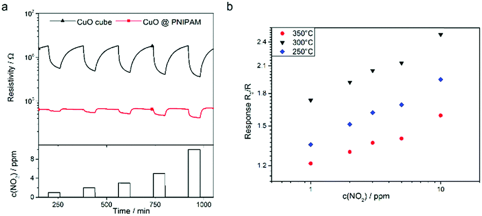 | ||
| Fig. 6 (a) Comparison of the sensing characteristics of bare CuO nanocubes (Ink solid content: 8 wt%) and CuO nanocubes from Cu2O@PNIPAM core–shell nanoparticles (ink solid content: 1.5 wt%) gas sensors towards increasing NO2 levels in dry synthetic air and an operating temperature of 300 °C. (b) Response characteristics of core–shell nanoparticle sensing devices for operation temperatures of 250 °C, 300 °C, and 350 °C respectively, which can be described by a typical power-law and reveal a distinct temperature dependency of sensitivity. | ||
As a measure for the response time we determine the time t90 it takes to achieve 90% of the new steady state value upon a change in the gas matrix. For the reaction of the functional layer towards NO2 and for recovering the baseline after removal of NO2 the Cu2O@PNIPAM nanoparticle derived layers are about 40% faster. While the bare Cu2O nanocube layers on average need t90,ads = 21.5 min for reacting to NO2 and t90,des = 91.9 min for recovering the baseline, the Cu2O@PNIPAM layer achieve t90,ads = 12.6 min and t90,des = 55.6 min, respectively.
Conclusions
In conclusion, the facile fabrication of CuO-based gas sensor with low material consumption and high sensitivity has been demonstrated by utilizing the Cu2O@PNIPAM core–shell microgels as novel ink system. The PNIPAM shell plays an essential role in the quest for the formation of uniform sensing layers and porous nanostructures. Firstly, the Cu2O@PNIPAM core–shell microgel dispersion shows significant improvement in colloidal stability and fluid properties compared with the native Cu2O nanocubes at room temperature. Thus, the aqueous dispersion of Cu2O@PNIPAM core–shell nanoparticles with low solid content (1.5 wt%) can be used directly as ink materials for the high resolution inkjet printing without introducing any other surfactants and organic solvents. Secondly, due to the protection of the PNIPAM shell, the uniform distribution of CuO nanoparticles can be preserved without merging into large aggregations after heating treatment. Gas sensing layers composed of hollow porous CuO nanocubes can be obtained after heat treatment at 350 °C for 60 min from the core–shell nanoparticles, which resulted in more sensitive gas sensor device. The remarkable improvements on high sensitivity and dodge of material wasting lie in the innovation strategy of modifying Cu2O nanocubes with PNIPAM shell, which can be extended to various inorganic nanomaterials.Conflicts of interest
There are no conflicts to declare.Acknowledgements
H. J. gratefully acknowledges financial support of the CSC scholarship. S. P. acknowledges funding from the Community of Madrid under grant number 2016-T1/AMB-1695. We also thank Dr Miriam Siebenbürger for her kind help for the rheological measurements and Prof. Jiayin Yuan for his professional suggestions about the modification of the manuscript.References
- C. Wang, L. Yin, L. Zhang, D. Xiang and R. Gao, Sensors, 2010, 10, 2088–2106 CrossRef PubMed.
- J.-K. Sun and Q. Xu, Energy Environ. Sci., 2014, 7, 2071 RSC.
- X. Liu, T. Ma, N. Pinna and J. Zhang, Adv. Funct. Mater., 2017, 27, 1–30 Search PubMed.
- F. Wang, H. Li, Z. Yuan, Y. Sun, F. Chang, H. Deng, L. Xie and H. Li, RSC Adv., 2016, 6, 79343–79349 RSC.
- J. Liu and D. Xue, Adv. Mater., 2008, 20, 2622–2627 CrossRef.
- J. Zhang, X. Liu, G. Neri and N. Pinna, Adv. Mater., 2016, 28, 795–831 CrossRef PubMed.
- Y. Sui, Y. Zeng, L. Fu, W. Zheng, D. Li, B. Liu and B. Zou, RSC Adv., 2013, 3, 18651 RSC.
- W. C. Huang, L. M. Lyu, Y. C. Yang and M. H. Huang, J. Am. Chem. Soc., 2012, 134, 1261–1267 CrossRef PubMed.
- C. G. Morales-Guio, S. D. Tilley, H. Vrubel, M. Grätzel and X. Hu, Nat. Commun., 2014, 5, 3059 CrossRef PubMed.
- C.-Y. Lin, Y.-H. Lai, D. Mersch and E. Reisner, Chem. Sci., 2012, 3, 3482 RSC.
- K. Chen, S. Song and D. Xue, CrystEngComm, 2015, 17, 2110–2117 RSC.
- J. C. Park, J. Kim, H. Kwon and H. Song, Adv. Mater., 2009, 21, 803–807 CrossRef.
- T. Jiang, T. Xie, W. Yang, H. Fan and D. Wang, J. Colloid Interface Sci., 2013, 405, 242–248 CrossRef PubMed.
- J. Zhang, J. Liu, Q. Peng, X. Wang and Y. Li, Chem. Mater., 2006, 18, 867–871 CrossRef.
- K. Henzler, A. Heilemann, J. Kneer, P. Guttmann, H. Jia, E. Bartsch, Y. Lu and S. Palzer, Sci. Rep., 2015, 5, 17729 CrossRef PubMed.
- J. Kneer, J. Wöllenstein and S. Palzer, Appl. Phys. Lett., 2014, 105 Search PubMed.
- J. Kneer, S. Knobelspies, B. Bierer, J. Wöllenstein and S. Palzer, Sens. Actuators, B, 2016, 222, 625–631 CrossRef.
- N. B. Tanvir, O. Yurchenko, C. Wilbertz and G. Urban, J. Mater. Chem. A, 2016, 4, 5294–5302 RSC.
- H. Gao, H. Jia, B. Bierer, J. Wöllenstein, Y. Lu and S. Palzer, Sens. Actuators, B, 2017, 249, 639–646 CrossRef.
- A. Chowdhuri, V. Gupta, K. Sreenivas, R. Kumar, S. Mozumdar and P. K. Patanjali, Appl. Phys. Lett., 2004, 84, 1180–1182 CrossRef.
- K. Sahner and H. L. Tuller, J. Electroceram., 2010, 24, 177–199 CrossRef.
- J. Li, S. Sollami Delekta, P. Zhang, S. Yang, M. R. Lohe, X. Zhuang, X. Feng and M. Östling, ACS Nano, 2017, 11, 8249–8256 CrossRef PubMed.
- W. Shen, X. Zhang, Q. Huang, Q. Xu and W. Song, Nanoscale, 2014, 6, 1622–1628 RSC.
- N. Marjanovic, J. Hammerschmidt, J. Perelaer, S. Farnsworth, I. Rawson, M. Kus, E. Yenel, S. Tilki, U. S. Schubert and R. R. Baumann, J. Mater. Chem., 2011, 21, 13634 RSC.
- H. O. Thomas Oehlund, Anna K. Schuppert, Magnus Hummelgard, Joakim Baeckstroem and Hans-Erik Nilsson, ACS Appl. Mater. Interfaces, 2015, 7, 18273–18282 CrossRef PubMed.
- F. Torrisi, T. Hasan, W. Wu, Z. Sun, A. Lombardo, T. S. Kulmala, G.-W. Hsieh, S. Jung, F. Bonaccorso, P. J. Paul, D. Chu and A. C. Ferrari, ACS Nano, 2012, 6, 2992–3006 CrossRef PubMed.
- D. Jang, D. Kim and J. Moon, Langmuir, 2009, 25, 2629–2635 CrossRef PubMed.
- W. Lee, Y. S. Lim, S. Kim, J. Jung, Y.-K. Han, S. Yoon, L. Piao and S.-H. Kim, J. Mater. Chem., 2011, 21, 6928 RSC.
- H. S. Lee and M. Y. Yang, IEEE Trans. Device Mater. Reliab., 2016, 16, 604–609 Search PubMed.
- T. T. Baby, S. K. Garlapati, S. Dehm, M. Ha, R. Kruk and H. Hahn, ACS Nano, 2015, 3075–3083 CrossRef PubMed.
- Y. X. Wang, X. F. Tang and Z. G. Yang, Colloids Surf., A, 2011, 388, 38–40 CrossRef.
- Z. Meng, J. K. Cho, V. Breedveld and L. A. Lyon, J. Phys. Chem. B, 2009, 113, 4590–4599 CrossRef PubMed.
- Y. Lu and M. Drechsler, Langmuir, 2009, 25, 13100–13105 CrossRef PubMed.
- M. Takizawa, Y. Sazuka, K. Horigome, Y. Sakurai, S. Matsui, H. Minato, T. Kureha and D. Suzuki, Langmuir, 2018, 34, 4515–4525 CrossRef PubMed.
- K. Horigome and D. Suzuki, Langmuir, 2012, 28, 12962–12970 CrossRef PubMed.
- B. Wedel, Y. Hertle, O. Wrede, J. Bookhold and T. Hellweg, Polymers, 2016, 8, 162 CrossRef.
- T. Hellweg, J. Polym. Sci., Part B: Polym. Phys., 2013, 51, 1073–1083 CrossRef.
- A. Balaceanu, Y. Verkh, D. Kehren, W. Tillmann and A. Pich, Z. Phys. Chem., 2014, 228, 253–267 Search PubMed.
- J. Pérez-Juste, I. Pastoriza-Santos and L. M. Liz-Marzán, J. Mater. Chem. A, 2013, 20–26 RSC.
- S. Jaber, M. Karg, A. Morfa and P. Mulvaney, Phys. Chem. Chem. Phys., 2011, 13, 5576–5578 RSC.
- H. Jia, R. Roa, S. Angioletti-Uberti, K. Henzler, A. Ott, X. Lin, J. Möser, Z. Kochovski, A. Schnegg, J. Dzubiella, M. Ballauff and Y. Lu, J. Mater. Chem. A, 2016, 4, 9677 RSC.
- J. E. Fromm, IBM J. Res. Dev., 1984, 28, 322–333 Search PubMed.
- A. Loutfi, S. Coradeschi, G. K. Mani, P. Shankar and J. B. B. Rayappan, J. Food Eng., 2015, 144, 103–111 CrossRef.
- A. D’Amico, G. Pennazza, M. Santonico, E. Martinelli, C. Roscioni, G. Galluccio, R. Paolesse and C. Di Natale, Lung Cancer, 2010, 68, 170–176 CrossRef PubMed.
- D. P. Volanti, A. A. Felix, M. O. Orlandi, G. Whitfield, D. J. Yang, E. Longo, H. L. Tuller and J. A. Varela, Adv. Funct. Mater., 2013, 23, 1759–1766 CrossRef.
- Y. Wang, Y. Lü, W. Zhan, Z. Xie, Q. Kuang and L. Zheng, J. Mater. Chem. A, 2015, 3, 12796–12803 RSC.
- Y. H. Choi, D. H. Kim and S. H. Hong, Sens. Actuators, B, 2017, 243, 262–270 CrossRef.
- A. Umar, A. A. Alshahrani, H. Algarni and R. Kumar, Sens. Actuators, B, 2017, 250, 24–31 CrossRef.
- P. Samarasekara, N. T. R. N. Kumara and N. U. S. Yapa, J. Phys.: Condens. Matter, 2006, 18, 2417–2420 CrossRef.
- C. H. Kuo, C. H. Chen and M. H. Huang, Adv. Funct. Mater., 2007, 17, 3773–3780 CrossRef.
- J. Kneer, A. Eberhardt, P. Walden, A. Ortiz Pérez, J. Wöllenstein and S. Palzer, Rev. Sci. Instrum., 2014, 85, 055006 CrossRef PubMed.
- P. Walden, J. Kneer, S. Knobelspies, W. Kronast, U. Mescheder and S. Palzer, J. Microelectromech. Syst., 2015, 24, 1384–1390 Search PubMed.
- R. D. Deegan, O. Bakajin, T. F. Dupont, G. Huber, S. R. Nagel and T. A. Witten, Nature, 1997, 389, 827–829 CrossRef.
- M. R. Alenezi, S. J. Henley, N. G. Emerson and S. R. P. Silva, Nanoscale, 2014, 6, 235–247 RSC.
- J. Kneer, S. Knobelspies, B. Bierer, J. Wöllenstein and S. Palzer, Sens. Actuators, B, 2016, 229, 57–62 CrossRef.
Footnote |
| † Electronic supplementary information (ESI) available. See DOI: 10.1039/c8tc01995a |
| This journal is © The Royal Society of Chemistry 2018 |