
 Open Access Article
 This Open Access Article is licensed under a
 Creative Commons Attribution 3.0 Unported Licence
Enhanced electrical properties of antimony doped tin oxide thin films deposited via aerosol assisted chemical vapour deposition†
Sapna D.
Ponja
a,
Benjamin A. D.
Williamson
 ab,
Sanjayan
Sathasivam
a,
David O.
Scanlon
abc,
Ivan P.
Parkin
a and
Claire J.
Carmalt
*a
ab,
Sanjayan
Sathasivam
a,
David O.
Scanlon
abc,
Ivan P.
Parkin
a and
Claire J.
Carmalt
*a
aMaterials Chemistry Centre, Department of Chemistry, University College London, 20 Gordon Street, London WC1H 0AJ, UK. E-mail: c.j.carmalt@ucl.ac.uk
bThomas Young Centre, University College London, Gower Street, London WC1E 6BT, UK
cDiamond Light Source Ltd, Diamond House, Harwell Science and Innovation Campus, Didcot, Oxfordshire OX11 0DE, UK
First published on 19th June 2018
Abstract
Transparent conducting oxides have widespread application in modern society but there is a need to move away from the current ‘industry champion’ tin doped indium oxide (In2O3:Sn) due to high costs. Antimony doped tin(IV) oxide (ATO) is an excellent candidate but is limited by its opto-electrical properties. Here, we present a novel and scalable synthetic route to ATO thin films that shows excellent electrical properties. Resistivity measurements showed that at 4 at% doping the lowest value of 4.7 × 10⁻⁴ Ω cm was achieved primarily due to a high charge carrier density of 1.2 × 1021 cm−3. Further doping induced an increase in resistivity due to a decrease in both the carrier density and mobility. Ab initio hybrid density functional theory (DFT) calculations show the thermodynamic basis for the tail off of performance beyond a certain doping level, and the appearance of Sb(III) within the doped thin films.
Introduction
The commercial significance of producing efficient and sustainable transparent conducting oxides (TCOs) cannot be underestimated. The excellent optoelectronic properties of TCO thin films are essential for a number of applications including solar cells, gas sensors, catalysis, electronics and optics.1,2 Thin films based on tin(IV) oxide have a wide fundamental band gap (∼3.6 eV) and a stability comparable to other TCO systems making them a viable alternative to the more expensive indium-tin oxide (ITO) films.3 The enhancement of electrical n-type conductivity properties can be achieved by the introduction of intrinsic defects, including oxygen vacancies, or by introducing extrinsic defects through aliovalent dopants with, for example, higher valency cations.4 The electrical resistivity is dependent on the density of charge carriers and their mobility5 and for nominally undoped SnO2 resistivity is limited to 10−2–10−3 Ω cm.1 Dopants such as fluorine and antimony have been used to great effect in improving the n-type conductivity of SnO2 films,6–11 with the latter dopant producing blue coloured coatings. However, it is not desirable to dope beyond a certain concentration as this is known to increase electrical resistivity and reduce optical transparency.12,13 Three general considerations needed when doping are: (i) the solubility of the dopant in the structure; (ii) shallowness of the dopant level; (iii) the dopant should not behave as a compensatory acceptor (a low energy electron killing defect).14 Antimony-doped tin oxide (ATO) materials have received particular attention due to the availability of the constituent metals and a recent increase in the demand for architectural coloured glass.7 The production of doped tin oxide films has been achieved by a variety of physical and chemical vapour deposition methods.1,10 Aerosol-assisted chemical vapour deposition (AACVD) is a low-cost and versatile technique with the potential to be scaled up for the commercial production of thin films.15 Unlike, other methods, AACVD negates the need for highly thermally stable and volatile precursors which widens the choice available for producing films with tuneable properties.16In this paper we doped tin(IV) oxide with varying concentrations of antimony. The as produced doped SnO2 structure contains Sb in the +3 and +5 states with Sb(V) responsible for the bluish colouration of the films.6,8,17 Our ATO thin films show significantly enhanced electrical properties with resistivities as low as 4.7 × 10⁻⁴, and to our knowledge are on par or superior to other published studies, on this material. A computational analysis into the role of intrinsic and Sb-related defects in SnO2 was carried out using hybrid density functional theory (DFT) and shows at low doping amounts, antimony is indeed incorporated into the lattice in the desired Sb(V) state.
Experimental
Deposition method
Depositions were carried in an atmosphere of air (BOC). The substrate used was SiO2 barrier coated float glass (15 cm × 4 cm × 0.3 cm; Pilkington Ltd, UK). The coating (ca. 50 nm in thickness) prevents the ions within the glass diffusing to the surface. Any surface grease on the glass was removed using a washing regime of detergent, propan-2-ol and acetone. The precursor solution consisting of 0.30 g butyltin trichloride and dopant amounts of antimony(III) ethoxide (all from Sigma-Aldrich) in 10 mL methanol was placed in a glass bubbler. An aerosol was generated using a piezo electric device and carried, in a flow of air (1 L min−1), through into horizontal bed cold-walled reactor (15 cm × 5 cm). The glass substrate, placed on the top and bottom of the reactor, was preheated to 450 °C on a graphite block containing a Whatman cartridge heater monitored by a Pt–Rh thermocouple. Depositions were achieved by the aerosol being carried in a stream of air through a brass baffle into the reactor. Waste vapours left through the exhaust. Once the entire precursor solution had been used up the reactor was allowed to cool to room temperature under air. Complete coverage of the substrate was achieved and the ATO films were blue and transparent with increasing dopant amounts in the precursor solution producing darker films.Film analysis
X-ray diffraction (XRD) measurements were obtained using a modified Bruker-Axs D8 diffractometer with parallel beam optics fitted with a PSD LynxEye silicon strip detector to collect diffracted X-ray photons. X-rays were generated using a Cu source with Cu Kα1 and Cu Kα2 radiation of wavelengths 1.54056 and 1.54439 Å, respectively, with an intensity ratio of 2![[thin space (1/6-em)]](https://www.rsc.org/images/entities/char_2009.gif) :1 and at 40 kV and 30 mA. The incident beam angle was kept at 1°, and the angular range of the patterns collected was 10° < 2θ < 66° with a step size of 0.05° counted at 4 s per step. The patterns were analysed for crystallinity and preferred orientation. Peak positions were compared to patterns from the Inorganic Crystal Structure Database (ICDS). The lattice parameters were calculated from powder X-ray diffraction data using the software GSAS and EXPGUI via the Le Bail method.
:1 and at 40 kV and 30 mA. The incident beam angle was kept at 1°, and the angular range of the patterns collected was 10° < 2θ < 66° with a step size of 0.05° counted at 4 s per step. The patterns were analysed for crystallinity and preferred orientation. Peak positions were compared to patterns from the Inorganic Crystal Structure Database (ICDS). The lattice parameters were calculated from powder X-ray diffraction data using the software GSAS and EXPGUI via the Le Bail method.
X-ray photoelectron spectroscopy (XPS) analysis of the films was carried out using a Thermo Scientific K-Alpha spectrometer equipped with a monochromatic Al-Kα source to identify chemical constituents. The peaks were modelled using CasaXPS software with binding energies adjusted to adventitious carbon (284.5 eV) in order to compensate for the effects of charging. Survey scans were collected in the range 0–1350 eV (binding energy) at a pass energy of 40 eV.
Wavelength dispersive X-ray (WDX) analysis was carried out on a Phillips ESEM. The Sn and Sb atomic% was derived from Sn-Kα line (25271.8 eV) and Sb-Kα (26359.5 eV), respectively.
UV/Vis/Near IR transmittance and reflectance spectra were produced using the Perkin Elmer Precisely Lambda 950 spectrometer using an air background and recorded between 320–2500 nm.
Scanning electron microscopy (SEM) was used to determine the film morphology from a top-down configuration using a JEOL JSM-6301F Field Emission instrument with accelerating voltages ranging from 3–5 keV on Au-coated samples. A side-on configuration was achieved using a JEOL JSM-6301F Field Emission instrument with accelerating voltages ranging from 5 keV on Au-coated samples.
Hall effect measurements were carried out on an Ecopia HMS-3000 set up in the Van der Pauw configuration to determine the sheet resistance, free carrier concentration (N) and mobility (μ). Samples of 1 cm2 were prepared and silver paint (Agar Scientific) was used to form ohmic contacts which were tested on the in-built software prior to measurement. The samples were then subjected to an input current of 1 mA and a calibrated magnetic field of 0.58 T.
Theoretical methodology
A computational analysis into the role of intrinsic and Sb-related defects in SnO2 was carried out using ab initio density functional theory (DFT) within the periodic code VASP.18–21 All geometrical and electronic optimisations were carried out using the hybrid functional PBE0 formalised by Adamo and Barone.22,23 PBE0 adds 25% of Hartree–Fock exchange to the PBE formalism resulting in an improved treatment of the self-interaction error compared to standard functionals. PBE0 can provide an accurate description of the band gap and geometry of SnO2 compared to experiment, and has been shown to accurately describe the properties of other tin-based oxides.24–33 The Projector Augmented Wave method (PAW)34 was used to account for the interaction between the core electrons and the valence electrons of each species (Sn[Kr], O[He], Sb[Kr]). Initially the conventional unit cell of rutile SnO2 was relaxed using a 400 eV plane-wave cutoff and a 4 × 4 × 6 Γ-centred k-point mesh to a force convergence tolerance of 0.01 eV atom−1.7 A supercell expansion of 2 × 2 × 3 (72 atoms) was produced to probe the properties of each defect and its respective charge states. Structural optimisations were undertaken relaxing only the ions within the cell, whilst keeping the cell parameters constant utilising a Γ-centred k-point mesh of 2 × 2 × 2 twinned with a 400 eV plane-wave energy cut-off. All calculations were spin-polarised and convergence was deemed to be complete when the forces acting on all the ions was less than 0.01 eV atom−1. Sb2O5, Sb2O4 and Sb2O3 were considered limiting phases in the formation of the dopant related species and were optimised using a planewave energy cut-off of 400 eV and Γ-centred k-point meshes of 2 × 5 × 4 (for the 28-atom Sb2O5 unit cell), 5 × 4 × 2 (for the 24 atom Sb2O4 unit cell) and 5 × 4 × 2 (for the 20 atom Sb2O3 unit cell). The volume, lattice parameters and atoms were allowed to relax until the forces acting on all ions was less than 0.01 eV atom−1.Defect formalism
The formation enthalpy for a defect in charge state ‘q’ was assessed using the relation:where ED,q is the total energy of the defective supercell in charge state ‘q’ and EH is the total energy of the host supercell. Ei and μi correspond to the elemental reference energies and the corresponding chemical potentials respectively (where ‘i’ = Sn(s), O2(g) and Sb(s)). n is either positive or negative depending on whether the element is taken away from or added to the system respectively. Ef is the Fermi energy and ranges from the valence band maximum (VBM) to ∼2.4 eV above the conduction band minimum (CBM) which occurs at 3.6 eV. εHVBM is the eigenvalue of the VBM of the host material and is aligned to the defective supercell via a potential alignment term (ΔEpot) which averages the total potential of the supercell bar that in the immediate vicinity of the defect.35

Due to the long ranged nature of the Coulomb interaction36,37 an image charge term q2EICcorr was applied to account for the interaction of a charged defect and its periodic images. The image charge correction used in this work is based upon the Lany and Zunger formalism35,38 with the ‘non-cubic’ adaptation as implemented by Hine and Murphy.39 For shallow and resonant defects, a band-filling correction (EBFcorr) was applied to regain the dilute limit due to the relatively high carrier concentrations present in supercell calculations.38,40
Thermodynamic limits
A chemical potential range can be applied to account for the extremes in growth conditions; Sn-rich/O-poor and Sn-poor/O-rich. These are set within the bounds of the calculated formation enthalpy of SnO2:41 | (1) |
| Sn-rich/O-poor conditions: μSn = 0 eV; μO = −2.64 eV s | (2.1) |
| Sn-poor/O-rich conditions: μSn = −5.27 eV; μO = 0 eV | (2.2) |
Therefore, μSb = −4.80 eV under Sn-poor/O-rich conditions.

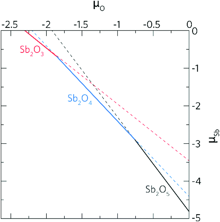 | ||
| Fig. 1 Phase stability diagram for the Sb-based oxides under varying μO and μSb. μO ranges from 0 eV (the formation of O2(g)) to −2.64 eV (the formation of Sn(s)). Under O-rich conditions Sb2O5 is the limiting phase and under O-poor conditions, Sb(s) is the limiting phase. | ||
The thermodynamic transition levels (q/q′) were defined as:
Results and discussion
The films were deposited via AACVD using butyltin trichloride and antimony(III) ethoxide, when doped, in methanol at 450 °C using air as the carrier gas. The doped films were blue in coloration, which darkened with increasing dopant concentration. They had excellent coverage across the glass substrate, were adherent (confirmed by the ScotchTM tape test) and air stable, showing no change over a one year period.The successful incorporation of Sb into the SnO2 films was confirmed by wavelength dispersive X-ray spectroscopy (WDX). The results show a positive correlation between the concentration of [Sb(OEt)3] in the precursor solution and the concentration in the films giving an average precursor efficiency of 47%.
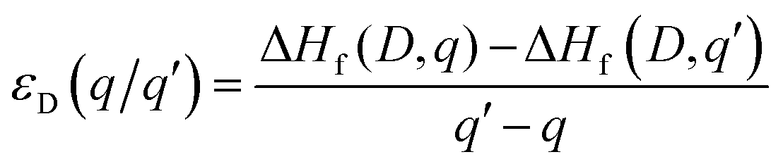
X-ray diffraction (XRD) carried out on the pure and Sb doped SnO2 films showed them to be phase pure and of the cassiterite phase with no peaks for SbOx observed even at high dopant concentrations therefore suggesting the successful formation of a solid solution (or a significant amorphous component). Le Bail modelling of the XRD patterns showed that doping of SnO2 with Sb generally results in a contraction of the cassiterite unit cell (Table 1). This follows what is expected for the substitutional doping of Sb5+ as its ionic radii is only 60 pm whereas Sn4+ is 69 pm. At high Sb doping concentration (10 at%) there was an increase in unit cell size compared to 4 and 7 at%, which was most likely due to incorporation of Sb3+ (radii of 76 pm) ions as well as the desired Sb5+ into the lattice.
| Film | Film thickness (nm) | Crystallite size (nm) | a (Å) | c (Å) | Unit cell volume (Å3) | χ2 | Fitted wRp |
|---|---|---|---|---|---|---|---|
| SnO2 | 480 | 16 | 4.7670(5) | 3.1902(2) | 72.493(14) | 2.1 | 17 |
| Sn0.99Sb0.01O2 | 550 | 23 | 4.7687(8) | 3.1945(2) | 72.643(23) | 2.4 | 18 |
| Sn0.96Sb0.04O2 | 525 | 19 | 4.7510(4) | 3.1935(2) | 72.081(11) | 1.7 | 14 |
| Sn0.93Sb0.07O2 | 800 | 25 | 4.7510(4) | 3.1915(2) | 72.041(11) | 2.0 | 17 |
| Sn0.90Sb0.10O2 | 800 | 23 | 4.7614(3) | 3.1944(1) | 72.421(8) | 2.2 | 16 |
Upon doping a change in the preferred orientation was also seen with doped samples showing less preference for the (101) and (301) planes and more for (002) planes of cassiterite. Doping also caused a slight increase in the crystallite size as estimated using the Deby–Scherrer equation (Table 1). This is not normally observed with the presence of dopants, as the addition of foreign ions into the host lattice usually causes a distortion and hence a decrease in crystallinity. The general trend of increased crystallite size with doping concentration as observed here maybe related to the increased film thickness (Fig. 2b–f). As these films were grown on amorphous glass substrates, layers in contact with and close to the substrate would be less crystalline and have smaller crystallite sizes. Due to templating effects the subsequent layers would then grow with larger crystallite sizes as these layers are now growing on crystalline layers beneath them. Therefore thicker films will on average have larger crystallite sizes. This effect has been previously observed for GaAs layers grown on glass via AACVD.42 Cross sectional high-resolution transmission electron spectroscopy (HRTEM) on the GaAs films found that crystallites close to the substrate were much smaller in size than the crystallites near the surface of the film.
 | ||
| Fig. 2 (a) XRD patterns of the as deposited and nominally Sb doped SnO2 thin films grown via AACVD. (b–f) Show the cross-sectional SEM images with the top down images as inset (scale bar for all images is equal to 500 nm). | ||
All the films consist of overlapping tooth like features that are top heavy. It was generally found that thicker films had larger widths of features at the top. Apart from this, the morphology of the films remained fairly consistent with thickness. Notably only one type of crystal growth was seen with no evidence of any amorphous features, strengthening the argument for a complete solid solution.
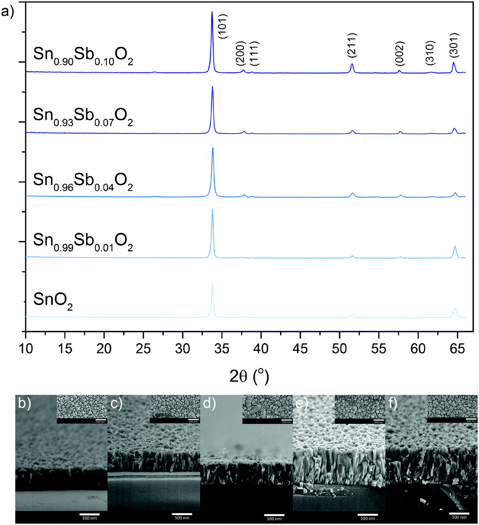
X-ray photoelectron spectra (Fig. 3a) showed the Sn 3d5/2 peak to correspond to literature examples of Sn(IV) and to be centred at 486.5 eV for all films apart from Sn0.96Sb0.04O2 that showed the peak to be slightly shifted to 486.1 eV.
 | ||
| Fig. 3 (a) Core level XPS spectra for the Sn 3d and Sb 3d signals. (b) Valence band spectra for all the AACVD grown films. | ||
The 3d5/2 peak for Sb overlaps with the O 1s but the less intense 3d3/2 can be used to confirm the presence of Sb in the films. The overlapping Sb 3d5/2 and O 1s peak was modelled with a spin orbit split of 9.39 eV and the Sb 3d5/2 peak intensity was 1.5 times greater than the Sb 3d3/2. Due to the similar peak positions of Sb(V) and Sb(III) it is difficult to differenciate between these two oxidation states with certainty from XPS alone, especially at dopant concentrations where signal to noise in the spectra can be low.
Valence band (VB) photoelectron spectra for the pure and Sb doped SnO2 films are shown in Fig. 3b. All spectra show the three peaks made up of O 2p states that are expected for the VB structure of SnO2. The overall O 2p band width is roughly 9 eV. Apart from some peak broadening there was not much change in the VB due to Sb doping. No electronic states were detected within the band gap as a result of doping, this is unusual as normally a peak is expected 0.5 eV below the Fermi level indicating conduction band filling upon semiconduction to metal transition. The absence of this peak maybe due to Sb being primarily a bulk dopant in the AACVD grown films. This also follows from core level XPS and WDX results that showed Sb levels at the surface being much lower than in the bulk therefore suggesting bulk segeration.
Hall effect measurements were taken at room temperature using the van der Pauw technique (Table 2). All the films showed n-type conductivity from the negative Hall coefficients. The resistivity, mobility and bulk concentration (charge carrier density) of undoped SnO2 were 1.8 × 10⁻³ Ω cm, 10.4 cm2 V−1 s−1 and 3.4 × 1020 cm−3, respectively, values which in general are in the ranges quoted in the literature, albeit, having produced the films through a range of techniques.1,43,44 The n-type conductivity is attributed to the formation of shallow donor levels occurring due to the presence of oxygen vacancies and interstitial tin in the SnO2 lattice.44,45 While the resistivity increased when 1 at% Sb was present in the SnO2 film, a doping level of 4 at% reduced the resistivity by a factor of 10. This was associated with an increase in mobility and carrier concentration which can be attributed to the ratio of Sb3+ and Sb5+ present in the lattice.46 The Sb5+ state contributes additional free electrons into the conduction band increasing conductivity and the charge carrier concentration.47 Above 4 at% Sb the resistivity increased with a corresponding decrease in mobility and carrier concentration. In such cases, more of the Sb5+ ions reduce to the Sb3+ state which act as acceptors hence removing electrons from the conduction band. Scattering of charge carriers limits mobility in polycrystalline materials.47,48 A possible reason for the decrease in carrier concentration in excess of 4 at% is due to the increased disorder that results from the donor having an increased activation energy.47
| Film | Film thickness (nm) | Sheet resistance (Ω sq−1) | Resistivity, ρ (Ω cm) | Mobility, μ (cm2 V−1 s−1) | Charge carrier concentration, N (cm−3) |
|---|---|---|---|---|---|
| SnO2 | 480 | 37.1 | 1.8 × 10⁻³ | 10.4 | 3.4 × 10²⁰ |
| Sn0.99Sb0.01O2 | 550 | 46.1 | 2.5 × 10⁻³ | 6.9 | 3.6 × 10²⁰ |
| Sn0.96Sb0.04O2 | 525 | 9.0 | 4.7 × 10⁻⁴ | 11.4 | 1.2 × 10²¹ |
| Sn0.93Sb0.07O2 | 800 | 20.2 | 1.6 × 10⁻³ | 6.2 | 6.2 × 10²⁰ |
| Sn0.90Sb0.10O2 | 880 | 39.1 | 3.4 × 10⁻³ | 3.1 | 5.8 × 10²⁰ |
The transmittance and reflectance spectra of the films were collected using visible/near IR spectroscopy between 320 and 2500 nm and are shown in Fig. 4. The undoped SnO2 film had the highest transmittance of up to 85% in the visible region. Doping Sb reduced the optimum transmittance in the visible range and increased reflectance in the infra-red. Transmittance decreased as a function of dopant level (from a maximum of 80% down to 45%). Correspondingly, the intensity of the blue colouration of the films increased which is commonly reported.6,17,49 However, a variety of explanations have been put forward to account for this observation to fit in with the opto-electronic properties of the films reported. One suggestion is that increasing the Sb dopant amounts leads to an increase in excitable electrons attributed to a greater presence of Sb5+.49 In contrast, others suggest, based on the observed reduction in conductivity that the darkening must be due to the presence of an increase in Sb3+ ions concentration.50
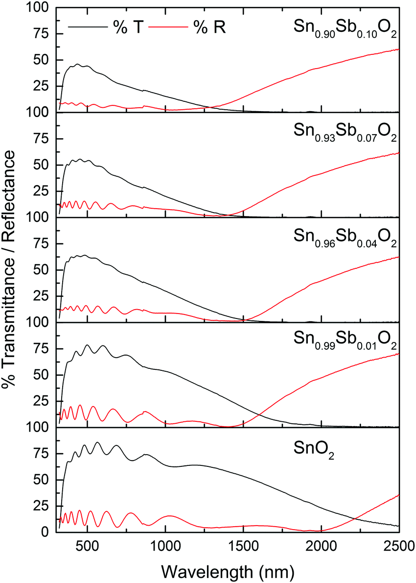 | ||
| Fig. 4 The transmittance (black) and reflectance (red) spectra of films produced via AACVD. | ||
The plasma edge was estimated from the energy at which the reflectivity reaches half its maximum value.3 In general, the plasma band onset of increased reflection shifted towards shorter wavelengths for the doped films compared with pure SnO2.
Emissivity is the ability of a material to emit infrared radiation; values range from 0 for a shiny mirror to 1 for a matt black body. For heat mirror applications reflection in the visible and near infrared are important. A low emissivity value is ideal for a heat mirror as reflection is high in the near infrared. The best commercially available TCO having heat mirror properties is Pilkington's fluorine tin oxide (FTO) having an emissivity value of 0.15. Emissivity normally drops with increasing dopant concentration reaching a minimum before increasing when more dopant is added. The emissivity of the undoped SnO2 film was 0.33. Doping with 1 at% Sb reduced the emissivity to 0.23, reaching a minimum of 0.22 at a dopant concentration of 7 at% and then increasing to 0.30 at the highest dopant concentration.
Computational analysis
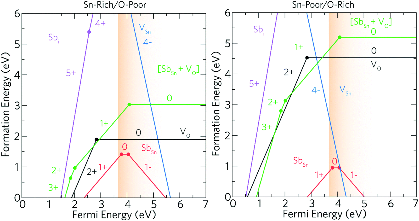
Ab initio density functional theory (DFT) was used to determine the role of both intrinsic and Sb dopant related defects on the electrical properties of SnO2.The thermodynamic transition levels are displayed in Fig. 5 and show the growth conditions under Sn-rich/O-poor (typically n-type favourable conditions) and Sn-poor/O-rich (p-type preferred conditions) and represent the extreme bounds of the equilibrium growth conditions. The dominant acceptor and donor intrinsic defects were modelled to aid the understanding of the Sb-related defects.
 | ||
| Fig. 5 The thermodynamic transition levels for Sn-rich/O-poor (left) and Sn-poor/O-rich (right). The Fermi energy ranges from the VBM (0 eV) to ∼3.4 eV above the CBM. The conduction band is depicted by the graded orange area. | ||
The oxygen and tin vacancies (VO and VSn) represent the dominant intrinsic donor and acceptor defects present in SnO2.24 VO is a low formation energy deep donor under Sn-rich/O-poor conditions, where the formation energy of the neutral charge state is ∼1.89 eV and rises to ∼4.53 eV under Sn-poor/O-rich conditions. As in other n-type oxides, such as ZnO31,51–53 and BaSnO3,29 VO is a negative-U defect32,54–56 with the 2+/0 transition level occurring ∼0.76 eV below the CBM in SnO2 revealing that VO will not contribute to the conductivity, which is supported by theoretical31,57,58 and experimental59,60 results alike. VSn also acts as a very deep acceptor with the 0/1− transition level occurring ∼1.75 eV above the VBM. VSn has a very high formation energy over the range of the band gap with the formation energy under the most favourable growth conditions (Sn-poor) being prohibitively high at ∼8.37 eV.
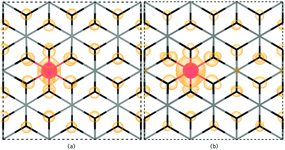
SbSn is a resonant donor with the 1+/0 transition level occurring ∼0.15 eV above the CBM and has a low formation energy under both Sn-rich/O-poor and Sn-poor/O-rich growth regimes. Interestingly, SbSn is highest in energy (ΔHf[Sb0Sn] = ∼1.42 eV) under typically n-type favourable “O-poor” conditions and lowest under a p-type favourable “O-rich” regime (ΔHf[Sb0Sn] = ∼0.95 eV). This is due to the lower μSn under Sn-poor/O-rich conditions and therefore the availability of free Sn sites. The facile incorporation of Sb, as found with the AACVD films here, is likely due to the similar ionic radii to Sn (Sn = 0.69 Å; Sb = 0.6(Sb5+)–0.76(Sb3+) Å)61 and over all charge states Sb is shown to have little distortion on the rutile lattice. Fig. 6a shows the partial charge density for Sb0Sn displaying a localization of the electron density in the Sb 5s orbital to the Sb defect. Under both growth conditions, the 0/1− transition level occurs ∼0.41 eV above the CBM and involves an extra electron being trapped on the Sb 5s orbital forming Sb3+ (Fig. 6b). As the defect states occur at the conduction band minimum there is small localization of density on O s states and Sn s states. Previous hybrid DFT calculations support a resonant low formation energy donor under both conditions,62–64 however Lany and co-workers propose that Sb is a negative U defect existing in only the 1− and 1+ charge states in contrast to our work.64
 | ||
| Fig. 6 The partial charge densities for (left) Sb0Sn and (right) Sb1−Sn as viewed along the (010) direction with a charge density of 0.005 eV A−1. For clarity, the Sn atoms (grey) and O atoms (black) are depicted by a stick model and the Sb (red) by a sphere. The electron charge density is shown in orange. | ||
The Sb–O bond lengths increase from ∼2.0 Å to ∼2.03 Å from the neutral to the 1− charge state so little distortion is seen. Under Sn-poor/O-rich conditions, Sb0Sn is compensated for by V4−Sn ∼ 0.45 eV above the CBM and at ∼2.05 eV under Sn-rich/O-poor conditions. Under both growth extremes therefore, the conductivity and mobilities in ATO films will be limited by the formation of the 0 and 1− charge state.
Extended X-ray absorption fine structure (EXAFS) have proposed the clustering of SbSn and VO leading to the formation of Sb3+ and a trapped electron in the VO site.65,66 [SbSn + VO] clusters were produced for this study in both a ‘near’ and ‘far’ configuration to examine this effect. The near configuration involved SbSn neighbouring a VO whilst the far configuration separated the two defects by ∼8 Å. From our calculations, we find that SbSn prefers to distort from its Sn site towards the oxygen vacancy with a binding energy of ∼0.78 eV. As such, higher Sb doping concentrations will facilitate the association of Sb with an oxygen vacancy. Typically, Coulombic effects should deter this behaviour from occurring considering that n-type defects should repel each other, however, this clustering is stabilised by the electronic rearrangement to give a lone pair on the Sb site. [SbSn + VO] in the far configuration is less energetically favourable than [SbSn + VO] in the near configuration by ∼0.4 eV.
Under Sn-rich/O-poor conditions, [SbSn + VO] is a shallow donor with a formation energy of ∼3.03 eV, this rises to ∼5.20 eV under an Sn-poor/O-rich regime. [SbSn + VO] acts as a one electron donor and has two transition levels deep in the bandgap, the 3+/2+ and 2+/1+ transition levels occur ∼1.75 eV and ∼1.59 eV below the CBM respectively. The 1+/0 transition level occurs ∼0.48 eV above the CBM. The partial charge densities for the neutral, 1+ and 2+ charge states are shown in Fig. 7a, b and c respectively. For the neutral charge state ([SbSn + VO]0), two electrons are located on a lone pair on Sb (indicating Sb(III)) with the remaining electron in the VO. This is consistent with the EXAFS analysis in which 5-coordinate Sb is seen corresponding to a removal of a neighbouring oxygen.65,66 In the 1+ charge state an electron is removed from the vacancy site leaving the two electrons in the Sb lone pair. The 2+ and 3+ charge states involve the subsequent removal of electrons from the lone pair as shown in Fig. 7b and c. As the 3+ and 2+ charge states are very deep in the band gap it is unlikely that these will be seen and as such there will be minimal effect on the optical transparency. It is therefore likely that Sb(III) will be seen for most situations where the Fermi level is greater than 2.01 eV. Sb hardly moves from its position over the range of charge states (maximum distortion of 2% in all three directions) despite the Sb ion originally distorting slightly towards the oxygen vacancy.
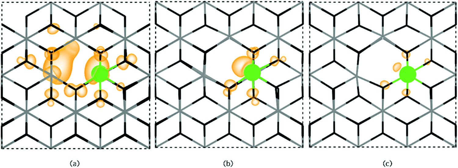 | ||
| Fig. 7 The partial charge densities for (a) [SbSn + VO]0 (b) [SbSn + VO]1+ and (c) [SbSn + VO]2+ as viewed along (010) using a charge density of 0.02 eV A−1. For clarity, the Sn atoms (grey) and O atoms (black) are depicted by a stick model and the Sb (green) by a sphere. The electron charge density is shown in orange. | ||
Under both growth regimes, Sbi is a very high formation energy donor, and is unlikely to form at Fermi levels near the CBM. Under Sn-rich/O-poor and Sn-poor/O-rich conditions, the formation energy of Sb0i is ∼9.40 eV and ∼14.20 eV respectively, and so quantities of Sbi are expected to be negligible.
Sb is therefore a low formation energy donor under both doping regimes and is expected to incorporate as Sb(V) at low doping concentrations. Towards higher concentrations, Sb may either form a localised polaron or likely have a preference to associate with an oxygen vacancy (VO) forming Sb(III) provided the concentration of oxygen vacancies are substantial. This defect complex, however, still donates an electron to the conduction band, accounting for the high conductivities in Sb-doped SnO2 samples here and elsewhere67 as well as the prevalence of Sb(III) and Sb(V) in the SnO2 lattice.
Conclusion
The AACVD prepared cassiterite phase pure ATO thin films using simple precursors at 450 °C show excellent optoelectrical properties. The best performing sample (4 at% Sb doped) showed an electrical resistivity of 4.7 × 10⁻⁴ Ω cm resulting from an electron mobility of 11.4 cm2 V−1 s−1 and a relatively high carrier density of 1.2 × 1021 cm−3. These results are comparable to some of the lowest resistivity values to date presented in literature for ATO hence having promising technological applications in optoelectronic devices. DFT calculations showed that at low doping concentrations, Sb incorporates into the SnO2 lattice as Sb(V). Sb(V) is a shallow donor with low formation energy. At higher doping regimes, the calculations show that substitutional Sb reduces to Sb(III) or associates with oxygen vacancies producing Sb(III) (present in the AACVD films) acting as a potential limitation to ATO thin films.Conflicts of interest
There are no conflicts to declare.Acknowledgements
This work made use of the ARCHER UK National Supercomputing Service (http://www.archer.ac.uk) via our membership of the UK's HEC Materials Chemistry Consortium, which is also funded by the EPSRC (EP/L000202). The UCL Legion and Grace HPC Facilities (Legion@UCL and Grace@UCL) were also used in the completion of this work. DOS would like to acknowledge support from the EPSRC (EP/N01572X/1). EPSRC are thanked for a studentship (SDP) and for grant no. EP/L017709. Simon Hurst, of Pilkington NSG, is thanked for emissivity calculations. NSG are thanked for the glass substrates.References
- Y.-Y. Lin, H.-Y. Lee, C.-S. Ku, L.-W. Chou and A. T. Wu, Bandgap narrowing in high dopant tin oxide degenerate thin film produced by atmosphere pressure chemical vapor deposition, Appl. Phys. Lett., 2013, 102(11), 111912 CrossRef.
- Y. Li, J. Wang, B. Feng, K. Duan and J. Weng, Synthesis and characterization of antimony-doped tin oxide (ATO) nanoparticles with high conductivity using a facile ammonia-diffusion co-precipitation method, J. Alloys Compd., 2015, 634, 37–42 CrossRef.
- D. S. Bhachu, D. O. Scanlon, G. Sankar, T. D. Veal, R. G. Egdell, G. Cibin, A. J. Dent, C. E. Knapp, C. J. Carmalt and I. P. Parkin, Origin of High Mobility in Molybdenum-Doped Indium Oxide, Chem. Mater., 2015, 27(8), 2788–2796 CrossRef.
- A. A. Yadav, S. C. Pawar, D. H. Patil and M. D. Ghogare, Properties of (200) oriented, highly conductive SnO2 thin films by chemical spray pyrolysis from non-aqueous medium: effect of antimony doping, J. Alloys Compd., 2015, 652, 145–152 CrossRef.
- L. Castañeda, Present status of the development and application of transparent conductors oxide thin solid films, Mater. Sci. Appl., 2011, 2, 1233–1242 Search PubMed.
- S. S. Lekshmy, G. P. Daniel and K. Joy, Microstructure and physical properties of sol gel derived SnO2:Sb thin films for optoelectronic applications, Appl. Surf. Sci., 2013, 274, 95–100 CrossRef.
- C. K. T. Chew, C. Salcianu, P. Bishop, C. J. Carmalt and I. P. Parkin, Functional thin film coatings incorporating gold nanoparticles in a transparent conducting fluorine doped tin oxide matrix, J. Mater. Chem. C, 2015, 3(5), 1118–1125 RSC.
- J. P. Correa Baena and A. G. Agrios, Transparent Conducting Aerogels of Antimony-Doped Tin Oxide, ACS Appl. Mater. Interfaces, 2014, 6(21), 19127–19134 CrossRef PubMed.
- K. Ravichandran and P. Philominathan, Analysis of critical doping level of sprayed antimony doped tin oxide films, J. Mater. Sci.: Mater. Electron., 2010, 22(2), 158–161 CrossRef.
- A. A. Yadav, Influence of film thickness on structural, optical, and electrical properties of spray deposited antimony doped SnO2 thin films, Thin Solid Films, 2015, 591(Part A), 18–24 CrossRef.
- C. Luan, Z. Zhu, W. Mi and J. Ma, Effect of Sb doping on structural, electrical and optical properties of epitaxial SnO2 films grown on r-cut sapphire, J. Alloys Compd., 2014, 586, 426–430 CrossRef.
- Y. Jiang, W. Sun, B. Xu, M. Yan and N. Bahlawane, Unusual enhancement in electrical conductivity of tin oxide thin films with zinc doping, Phys. Chem. Chem. Phys., 2011, 13(13), 5760–5763 RSC.
- Z. Banyamin, P. Kelly, G. West and J. Boardman, Electrical and Optical Properties of Fluorine Doped Tin Oxide Thin Films Prepared by Magnetron Sputtering, Coatings, 2014, 4(4), 732 CrossRef.
- J. Robertson and B. Falabretti, Electronic Structure of Transparent Conducting Oxides, in Handbook of Transparent Conductors, ed. Ginley, D. S., Springer US, Boston, MA, 2011, pp. 27–50 Search PubMed.
- M. J. Powell and C. J. Carmalt, Aerosols: A Sustainable Route to Functional Materials, Chem. – Eur. J., 2017, 23(62), 15543–15552 CrossRef PubMed.
- P. Marchand, I. A. Hassan, I. P. Parkin and C. J. Carmalt, Aerosol-assisted delivery of precursors for chemical vapour deposition: expanding the scope of CVD for materials fabrication, Dalton Trans., 2013, 42(26), 9406–9422 RSC.
- E. Elangovan and K. Ramamurthi, A study on low cost-high conducting fluorine and antimony-doped tin oxide thin films, Appl. Surf. Sci., 2005, 249(1–4), 183–196 CrossRef.
- G. Kresse and J. Hafner, Ab initio molecular dynamics for liquid metals, Phys. Rev. B: Condens. Matter Mater. Phys., 1993, 47(1), 558–561 CrossRef.
- G. Kresse and J. Hafner, Ab Initio Molecular-Dynamics Simulation of the Liquid-Metal–Amorphous-Semiconductor Transition in Germanium, Phys. Rev. B: Condens. Matter Mater. Phys., 1994, 49, 14251 CrossRef.
- G. Kresse and J. Furthmüller, Efficiency of ab-initio total energy calculations for metals and semiconductors using a plane-wave basis set, Comput. Mater. Sci., 1996, 6(1), 15–50 CrossRef.
- G. Kresse and J. Furthmüller, Efficient iterative schemes for ab initio total-energy calculations using a plane-wave basis set, Phys. Rev. B: Condens. Matter Mater. Phys., 1996, 54(16), 11169–11186 CrossRef.
- C. Adamo and V. Barone, Toward reliable density functional methods without adjustable parameters: the PBE0 model, J. Chem. Phys., 1999, 110(13), 6158–6170 CrossRef.
- J. Paier, R. Hirschl, M. Marsman and G. Kresse, The Perdew–Burke–Ernzerhof exchange-correlation functional applied to the G2-1 test set using a plane-wave basis set, J. Chem. Phys., 2005, 122(23), 234102 CrossRef PubMed.
- D. O. Scanlon and G. W. Watson, On the possibility of p-type SnO2, J. Mater. Chem., 2012, 22(48), 25236–25245 RSC.
- A. M. Ganose and D. O. Scanlon, Band gap and work function tailoring of SnO2 for improved transparent conducting ability in photovoltaics, J. Mater. Chem. C, 2016, 4(7), 1467–1475 RSC.
- S. K. Vasheghani Farahani, T. D. Veal, J. J. Mudd, D. O. Scanlon, G. W. Watson, O. Bierwagen, M. E. White, J. S. Speck and C. F. McConville, Valence-band density of states and surface electron accumulation in epitaxial SnO2 films, Phys. Rev. B: Condens. Matter Mater. Phys., 2014, 90(15), 155413 CrossRef.
- Z. Lebens-Higgins, D. O. Scanlon, H. Paik, S. Sallis, Y. Nie, M. Uchida, N. F. Quackenbush, M. J. Wahila, G. E. Sterbinsky, D. A. Arena, J. C. Woicik, D. G. Schlom and L. F. J. Piper, Direct Observation of Electrostatically Driven Band Gap Renormalization in a Degenerate Perovskite Transparent Conducting Oxide, Phys. Rev. Lett., 2016, 116(2), 027602 CrossRef PubMed.
- S. Sallis, D. O. Scanlon, S. C. Chae, N. F. Quackenbush, D. A. Fischer, J. C. Woicik, J. H. Guo, S. W. Cheong and L. F. J. Piper, La-doped BaSnO3—Degenerate perovskite transparent conducting oxide: evidence from synchrotron X-ray spectroscopy, Appl. Phys. Lett., 2013, 103(4), 042105 CrossRef.
- D. O. Scanlon, Defect engineering of BaSnO${ }_{3}$ for high-performance transparent conducting oxide applications, Phys. Rev. B: Condens. Matter Mater. Phys., 2013, 87(16), 161201 CrossRef.
- J. Suffner, P. Ágoston, J. Kling and H. Hahn, Chemical vapor synthesis of fluorine-doped SnO2 (FTO) nanoparticles, J. Nanopart. Res., 2010, 12(7), 2579–2588 CrossRef.
- P. Ágoston, K. Albe, R. M. Nieminen and M. J. Puska, Intrinsic n-Type Behavior in Transparent Conducting Oxides: A Comparative Hybrid-Functional Study of In2O3, SnO2, and ZnO, Phys. Rev. Lett., 2009, 103(24), 245501 CrossRef PubMed.
- J. P. Allen, D. O. Scanlon, L. F. J. Piper and G. W. Watson, Understanding the defect chemistry of tin monoxide, J. Mater. Chem. C, 2013, 1(48), 8194–8208 RSC.
- N. F. Quackenbush, J. P. Allen, D. O. Scanlon, S. Sallis, J. A. Hewlett, A. S. Nandur, B. Chen, K. E. Smith, C. Weiland, D. A. Fischer, J. C. Woicik, B. E. White, G. W. Watson and L. F. J. Piper, Origin of the Bipolar Doping Behavior of SnO from X-ray Spectroscopy and Density Functional Theory, Chem. Mater., 2013, 25(15), 3114–3123 CrossRef.
- P. E. Blöchl, Projector Augmented-Wave Method, Phys. Rev. B: Condens. Matter Mater. Phys., 1994, 50, 17953 CrossRef.
- L. Stephan and Z. Alex, Accurate prediction of defect properties in density functional supercell calculations, Modell. Simul. Mater. Sci. Eng., 2009, 17(8), 084002 CrossRef.
- N. D. M. Hine, K. Frensch, W. M. C. Foulkes and M. W. Finnis, Supercell size scaling of density functional theory formation energies of charged defects, Phys. Rev. B: Condens. Matter Mater. Phys., 2009, 79(2), 024112 CrossRef.
- M. N. Risto, Issues in first-principles calculations for defects in semiconductors and oxides, Modell. Simul. Mater. Sci. Eng., 2009, 17(8), 084001 CrossRef.
- S. Lany and A. Zunger, Assessment of correction methods for the band-gap problem and for finite-size effects in supercell defect calculations: case studies for ZnO and GaAs, Phys. Rev. B: Condens. Matter Mater. Phys., 2008, 78(23), 235104 CrossRef.
- S. T. Murphy and N. D. M. Hine, Point Defects and Non-stoichiometry in Li2TiO3, Chem. Mater., 2014, 26(4), 1629–1638 CrossRef.
- C. Freysoldt, J. Neugebauer and C. G. Van de Walle, Fully Ab Initio Finite-Size Corrections for Charged-Defect Supercell Calculations, Phys. Rev. Lett., 2009, 102(1), 016402 CrossRef PubMed.
- D. R. Lide, CRC Handbook of Chemistry and Physics, Internet version, CRC Press, Boca Raton, FL, 2005 Search PubMed.
- S. Sathasivam, R. R. Arnepalli, D. S. Bhachu, Y. Lu, J. Buckeridge, D. O. Scanlon, B. Kumar, K. K. Singh, R. J. Visser, C. S. Blackman and C. J. Carmalt, Single Step Solution Processed GaAs Thin Films from GaMe3 and tBuAsH2 under Ambient Pressure, J. Phys. Chem. C, 2016, 120(13), 7013–7019 CrossRef.
- A. Oprea, E. Moretton, N. Bârsan, W. J. Becker, J. Wöllenstein and U. Weimar, Conduction model of SnO2 thin films based on conductance and Hall effect measurements, J. Appl. Phys., 2006, 100(3), 033716 CrossRef.
- K. H. Kim and S. W. Lee, Effect of antimony addition on electrical and optical properties of tin oxide film, J. Am. Ceram. Soc., 1994, 77, 915–921 CrossRef.
- I. Saadeddin, H. S. Hilal, B. Pecquenard, J. Marcus, A. Mansouri, C. Labrugere, M. A. Subramanian and G. Campet, Simultaneous doping of Zn and Sb in SnO2 ceramics: enhancement of electrical conductivity, Solid State Sci., 2006, 8(1), 7–13 CrossRef.
- S. Gupta, B. C. Yadav, P. K. Dwivedi and B. Das, Microstructural, optical and electrical investigations of Sb-SnO2 thin films deposited by spray pyrolysis, Mater. Res. Bull., 2013, 48(9), 3315–3322 CrossRef.
- M. Esro, S. Georgakopoulos, H. Lu, G. Vourlias, A. Krier, W. I. Milne, W. P. Gillin and G. Adamopoulos, Solution processed SnO2:Sb transparent conductive oxide as an alternative to indium tin oxide for applications in organic light emitting diodes, J. Mater. Chem. C, 2016, 4(16), 3563–3570 RSC.
- R. Vázquez-Arreguín, M. Aguilar-Frutis, C. Falcony-Guajardo, A. Castañeda-Galván, L. Mariscal-Becerra, S. Gallardo-Hernández, G. Alarcón-Flores and M. García-Rocha, Electrical, Optical and Structural Properties of SnO2:Sb:F Thin Films Deposited from Sn(acac)2 by Spray Pyrolysis, ECS J. Solid State Sci. Technol., 2016, 5(3), Q101–Q107 CrossRef.
- D.-W. Jung and D.-W. Park, Synthesis of nano-sized antimony-doped tin oxide (ATO) particles using a DC arc plasma jet, Appl. Surf. Sci., 2009, 255(10), 5409–5413 CrossRef.
- M. Kojima, H. Kato and M. Gatto, Blackening of tin oxide thin films heavily doped with antimony, Philos. Mag. B, 1993, 68(2), 215–222 Search PubMed.
- F. Oba, M. Choi, A. Togo and I. Tanaka, Point defects in ZnO: an approach from first principles, Sci. Technol. Adv. Mater., 2011, 12(3), 034302 CrossRef PubMed.
- F. Oba, S. R. Nishitani, S. Isotani, H. Adachi and I. Tanaka, Energetics of native defects in ZnO, J. Appl. Phys., 2001, 90(2), 824–828 CrossRef.
- A. Janotti and C. G. Van de Walle, Native point defects in ZnO, Phys. Rev. B: Condens. Matter Mater. Phys., 2007, 76(16), 165202 CrossRef.
- A. Walsh, C. R. A. Catlow, A. A. Sokol and S. M. Woodley, Physical Properties, Intrinsic Defects, and Phase Stability of Indium Sesquioxide, Chem. Mater., 2009, 21(20), 4962–4969 CrossRef.
- S. Lany and A. Zunger, Polaronic hole localization and multiple hole binding of acceptors in oxide wide-gap semiconductors, Phys. Rev. B: Condens. Matter Mater. Phys., 2009, 80(8), 085202 CrossRef.
- A. Goyal, P. Gorai, H. Peng, S. Lany and V. Stevanović, A computational framework for automation of point defect calculations, Comput. Mater. Sci., 2017, 130(Suppl C), 1–9 CrossRef.
- P. Ágoston, C. Körber, A. Klein, M. J. Puska, R. M. Nieminen and K. Albe, Limits for n-type doping in In2O3 and SnO2: A theoretical approach by first-principles calculations using hybrid-functional methodology, J. Appl. Phys., 2010, 108(5), 053511 CrossRef.
- A. K. Singh, A. Janotti, M. Scheffler and C. G. Van de Walle, Sources of Electrical Conductivity in SnO2, Phys. Rev. Lett., 2008, 101(5), 055502 CrossRef PubMed.
- S. Samson and C. G. Fonstad, Defect structure and electronic donor levels in stannic oxide crystals, J. Appl. Phys., 1973, 44(10), 4618–4621 CrossRef.
- P. D. C. King, R. L. Lichti, Y. G. Celebi, J. M. Gil, R. C. Vilão, H. V. Alberto, J. Piroto Duarte, D. J. Payne, R. G. Egdell, I. McKenzie, C. F. McConville, S. F. J. Cox and T. D. Veal, Shallow donor state of hydrogen in In2O3 and SnO2: implications for conductivity in transparent conducting oxides, Phys. Rev. B: Condens. Matter Mater. Phys., 2009, 80(8), 081201 CrossRef.
- R. D. Shannon, Revised effective ionic radii and systematic studies of interatomic distances in halides and chalcogenides, Acta Crystallogr., Sect. A: Cryst. Phys., Diffr., Theor. Gen. Crystallogr., 1976, 32, 751–767 CrossRef.
- M. Behtash, P. H. Joo, S. Nazir and K. Yang, Electronic structures and formation energies of pentavalent-ion-doped SnO2: first-principles hybrid functional calculations, J. Appl. Phys., 2015, 117(17), 175101 CrossRef.
- J. B. Varley, A. Janotti and C. G. Van de Walle, Group-V impurities in SnO2 from first-principles calculations, Phys. Rev. B: Condens. Matter Mater. Phys., 2010, 81(24), 245216 CrossRef.
- H. Peng, J. D. Perkins and S. Lany, Multivalency of Group 15 Dopants in SnO2, Chem. Mater., 2014, 26(16), 4876–4881 CrossRef.
- V. Geraldo, V. Briois, L. V. A. Scalvi and C. V. Santilli, EXAFS investigation on Sb incorporation effects to electrical transport in SnO2 thin films deposited by sol–gel, J. Eur. Ceram. Soc., 2007, 27(13), 4265–4268 CrossRef.
- J. Rockenberger, U. zum Felde, M. Tischer, L. Tröger, M. Haase and H. Weller, Near edge X-ray absorption fine structure measurements (XANES) and extended x-ray absorption fine structure measurements (EXAFS) of the valence state and coordination of antimony in doped nanocrystalline SnO2, J. Chem. Phys., 2000, 112(9), 4296–4304 CrossRef.
- K. Y. Rajpure, M. N. Kusumade, M. N. Neumann-Spallart and C. H. Bhosale, Effect of Sb doping on properties of conductive spray deposited SnO2 thin films, Mater. Chem. Phys., 2000, 64(3), 184–188 CrossRef.
Footnote |
| † Electronic supplementary information (ESI) available. See DOI: 10.1039/c8tc01929k |
| This journal is © The Royal Society of Chemistry 2018 |