
 Open Access Article
 This Open Access Article is licensed under a
 Creative Commons Attribution 3.0 Unported Licence
Technique and model for modifying the saturable absorption (SA) properties of 2D nanofilms by considering interband exciton recombination†
Guowen
Liang‡
a,
Longhui
Zeng‡
b,
Yuen Hong
Tsang
*b,
Lili
Tao
b,
Chun Yin
Tang
b,
Ping Kwong
Cheng
b,
Hui
Long
b,
Xin
Liu
a,
Ji
Li
a,
Junle
Qu
 a and
Qiao
Wen
*a
a and
Qiao
Wen
*a
aKey Laboratory of Optoelectronic Devices and Systems of Ministry of Education and Guangdong Province, College of Optoelectronic Engineering, Shenzhen University, Shenzhen 518060, China. E-mail: wenqiao@szu.edu.cn
bDepartment of Applied Physics and Materials Research Center, The Hong Kong Polytechnic University, Kowloon, Hong Kong, China. E-mail: yuen.tsang@polyu.edu.hk
First published on 30th April 2018
Abstract
In this study, we have successfully demonstrated a method of greatly modifying the nonlinear saturable absorption (SA) properties of WS2 nanofilms by controlling their thickness and morphology via magnetron sputtering deposition times. The nonlinear SA properties of these nanofilms were also investigated systematically under excitation by laser pulses with various durations in the fs, ps and ns ranges, and prominent ultrafast SA parameters were demonstrated for different pulse durations in the fs, ps and ns ranges. A pulse width-dependent theoretical model of SA that considers the effects of interband exciton recombination has now been proposed for the first time. Two analytical expressions for calculating the variation of key SA parameters (the onset fluence Fon and the modulation depth ΔT) with the excitation laser pulse width have been derived and experimentally verified. The theoretical model and analytical expressions have great value for understanding and interpreting the variation of the SA behaviors of 2D nanofilms in the fs, ps and ns regions, and for the developments of ultrafast lasers and nanosecond lasers based on 2D materials. These studies open up exciting avenues for engineering the SA properties of 2D nanofilms for a wide range of laser photonic devices and applications.
1 Introduction
Two-dimensional (2D) layered materials are currently attracting great research interest and attention from the optics, laser, photonics and optoelectronics research communities for their potential to bring revolutionary changes to these fields. 2D materials exhibit exceptional electrical and optical properties compared to their bulk forms due to the quantum confinement perpendicular to the 2D plane.1 Soon after the discovery of graphene in 2004,2,3 scientists demonstrated advanced electric and photonic applications such as photodetectors,4–8 light-emitting diodes,9 phototransistors,10,11 solar cells,12 optical waveguides,13 and ultrafast lasers14 by using graphene. However, the zero-bandgap nature and low layer optical absorption of graphene limits its application in the field of photonics and nonlinear optics. Therefore, the research focus has been extended to other 2D materials15–18 with natural bandgaps. In the past few years, the emergence of 2D transition metal dichalcogenides (TMDs), e.g., MX2 (M = Mo, W; X = S, Se), has attracted increasing attention because of their wide bandgap range from near-infrared to the visible region19 and their unique and favorable electrical, optical, thermal and mechanical properties.20 Layered TMDs are a new class of functional materials and have been used extensively in various applications such as nanoelectronics,21 solar cells,22 photodetectors,23 nonlinear optics24–26 photocatalysis27 and energy storage.28 Molybdenum disulfide (MoS2) is the most studied member of the TMD family for nonlinear optical applications,29–31 and very recently, the novel tungsten disulfide (WS2) began to receive significant attention because of its tunable bandgap arising from indirect-to-direct bandgap transition with a decreasing number of layers, high carrier mobility and strong spin–orbit coupling due to its asymmetric structure and favorable photonic properties.32,33 WS2 exhibits strong nonlinear optical limiting properties and is tunable by adjustment of the size and thickness.24 Therefore, the saturable absorption (SA) properties of these novel 2D materials are an important research topic, as the mainstream saturable absorbers used for Q-switching and mode locking, e.g., doped crystals and SESAMs, still have some limitations such as narrow operation wavebands, limited response times, high cost, and complex fabrication processes.34,35 A previous study confirmed that WS2 exhibits strong SA properties and an ultrahigh optical damage threshold with a broad operational wavelength range from the visible range36–38 up to the mid infrared range;39,40 therefore, Q-switching32,34,36–38,40–45 and mode locking32,35,39,46–48 laser pulses can be generated by utilizing WS2 as a saturable absorber in various laser systems. The fabrication of WS2 film is relatively simple and low cost compared with that of the mainstream saturable absorbers used in commercial pulsed laser products.Additionally, WS2 and other new TMDs, can be widely used in other photonic device applications, e.g., optical communications and optical computing.49 The performance of such devices is largely dependent upon the nonlinear optical parameters of the 2D SA materials, and therefore, tuning and characterizing the parameters of 2D SA properties has become a highly important research topic for various nonlinear optical applications.50–53 For the above reasons, this research aims to examine the SA properties of TMDs with different film thicknesses and structures for different pulse durations and lifetimes.
In this study, polycrystalline WS2 film samples with various thicknesses were fabricated by the magnetron sputtering deposition method because of its high production speed and scalability compared with the CVD method. The WS2 film thickness and structure depend on the sputtering time. The SA properties of the WS2 films were then investigated under excitation by an 800 nm laser pulse with various pulse widths (100 fs, 10 ps, 200 ps, 10 ns) but the same pulse energy by using an open aperture (OA) Z-scan method. A theoretical model showing the relationship between the key SA parameters and the excitation pulse width, considering the effects of interband exciton recombination, was developed for the first time, and analytical expressions for the variation of these key SA parameters with the pulse width were deduced. The expressions were experimentally verified by Z-scan experiments. These analytical expressions provide a new way to estimate the SA parameters of any TMD film for various ultrafast pulse duration ranges. These studies will allow us to gain deeper understanding for engineering the nonlinear SA properties of the 2D materials and will significantly benefit the development of 2D materials for a wide range of nonlinear optical applications, including passive mode-lockers, passive Q-switchers, optical switches, ultrafast pulse shaping devices, and optical signal processing devices used in optical communication systems and optical computing.
2 Sample preparation and characteristics
The WS2 samples used for this experiment were fabricated by the magnetron sputtering of WS2 onto a clean quartz substrate for various periods of time (1 min, 3 min and 5 min) to control its film thickness followed by post-annealing. WS2 precursor films were first produced through sputtering by using a sintered WS2 disk as the target. The post annealing process was then conducted to enhance the crystallinity of the WS2 film and replenish the S contents in the WS2. Fig. 1(a) displays photographs of post-annealed polycrystalline WS2 film on a quartz substrate, showing a characteristic change from dark gray to yellow and yellowish green. The transmittance spectra of WS2 films with different thicknesses are presented in Fig. 1(b), which clearly shows absorption characteristic peaks located between 600 and 650 nm. The characteristic absorption peaks of WS2 films fabricated with different sputtering times (1 min, 3 min, and 5 min) were located at 644.5 nm, 632 nm and 629 nm, respectively. The differences in peak position between samples indicate that polycrystalline WS2 films with different thicknesses and morphologies can be fabricated by controlling the magnetron sputtering time. The transmittance spectra showed that the peak position of the WS2 film shifts to shorter wavelengths as the sputtering time increases.54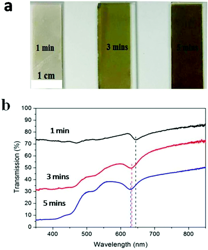 | ||
| Fig. 1 (a) Photographs and (b) transmission spectra of WS2 films fabricated with different magnetron sputtering times. | ||
The surface topography of the WS2 films was investigated by atomic force microscopy (AFM) measurement as shown in Fig. 2(a–c), which revealed that all the WS2 films were continuous. The corresponding section height profiles of the WS2 samples were measured and are shown in Fig. 2(d–f). The measured film thicknesses were 8.85 nm, 15.7 nm, and 27.7 nm for the 1 min, 3 min and 5 min WS2 films, respectively.
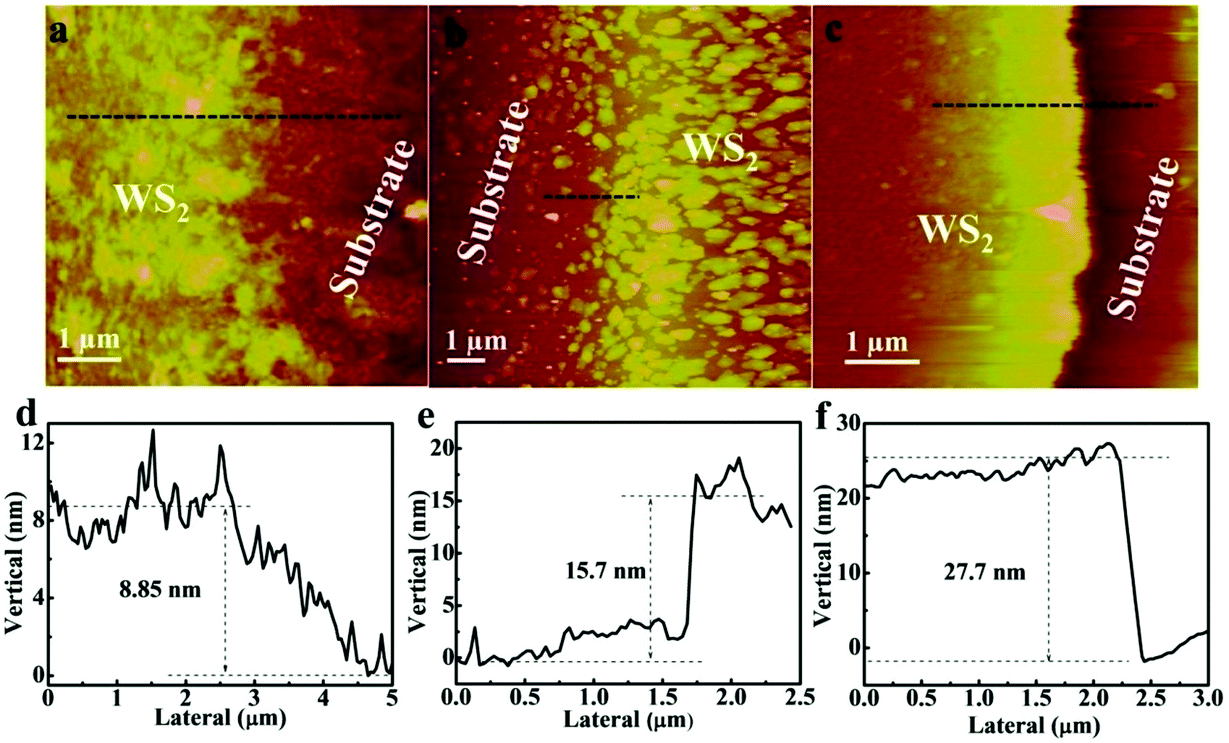 | ||
| Fig. 2 (a–c) AFM images of WS2 films; (d–f) height profiles of WS2 films obtained with 1 min, 3 min and 5 min sputtering time, respectively. | ||
Raman spectroscopy is a powerful tool for the investigation of the crystal structures and layer numbers of the WS2 films. Therefore, Raman mappings of all the WS2 films samples were recorded and are shown in Fig. 3. As expected, the WS2 samples show two strong signals due to the in-plane vibration E12g of the tungsten and sulfur atoms and the out-of-plane vibration A1g of the sulfur atoms. Both dominant Raman modes with wave numbers of approximately 350 cm−1 and 420 cm−1, respectively, can be identified in Fig. 3, which is in good agreement with the results found in previous reports.55 According to previous reports, the frequency difference between the E12g and A1g modes of TMDs, Δω, is dependent on the average layer number.56 In general, Δω decreases as the average layer number decreases.57 The measured Δω values of the 1 min, 3 min and 5 min WS2 samples were 65.7 cm−1, 65 cm−1 and 64.2 cm−1 respectively. These results confirm that the 1 min WS2 film contained a higher number of layers than the 3 and 5 min films. In conclusion, the layer numbers of WS2 films fabricated with sputtering times of 3 min and 5 min are similar and are lower than the layer number of 1 min WS2 film.
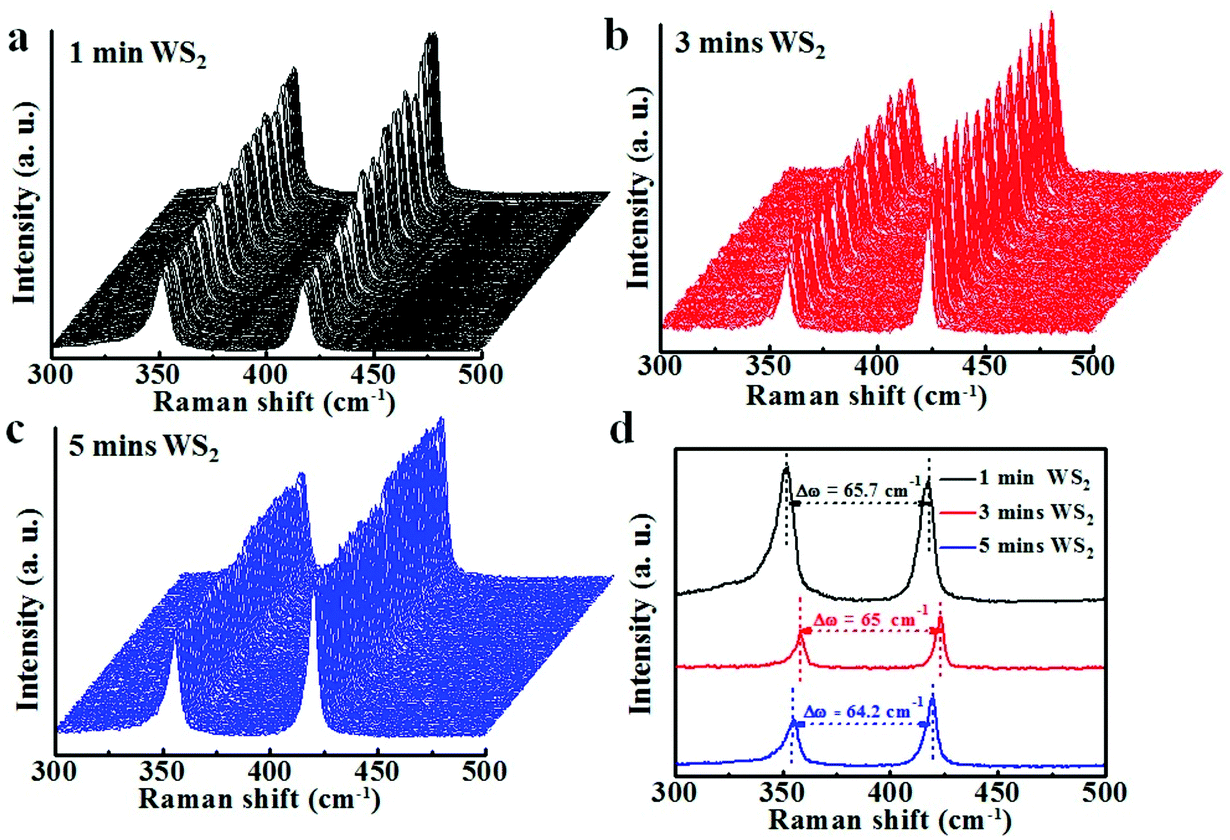 | ||
| Fig. 3 Raman spectra of WS2 films extracted from the Raman mapping data obtained in 10 × 10 μm2 regions of (a) 1 min, (b) 3 min and (c) 5 min WS2 films. (d) Typical Raman spectra of WS2 films showing the average frequency difference, Δω. | ||
Transmission electron microscopy (TEM) was employed to characterize the layer number, crystallinity and structure of the WS2 samples, as shown in Fig. 4(a, d and g) TEM and Fig. 4(b, e and h) high-resolution transmission electron microscopy (HRTEM) images. The energy-dispersive X-ray spectroscopy (EDS) spectra of three samples are shown in Fig. 4(c, f and i). These results showed that the 1 min WS2 film consisted of large-area polycrystalline WS2 film, but countless WS2 nanosheets were found within the 3 min and 5 min WS2 films. The results also showed that the 1 min and 3 min WS2 sheets were mainly horizontally grown, while the 5 min films contained many vertically grown sheets, as shown in Fig. 4(g and h). The change in growth direction from horizontal to vertical is directly related to the amount of WS2 deposited on the substrate – the thickness of the precursor WS2 films. During post-annealing, sulfur vapor diffused into very thin amorphous WS2 layers; the horizontal growth of large-area WS2 was more energetically favorable than the growth of vertically aligned layers because WS2 films with horizontal growth exposed low-surface-energy basal planes. However, when thick amorphous WS2 films undergo post-annealing, horizontal volume expansion cannot be easily accommodated due to the precursor films anchored to the substrate. In this case, the horizontal growth of a large size and continuous film will produce a great deal of strain energy, and therefore, WS2 films would grow vertically because of the unconstrained free volume expansion in the vertical direction.58,59 Moreover, the HRTEM images in Fig. 3(b, e and h) show horizontally grown WS2 sheets with 0.28 nm interplane spacing and vertically grown WS2 sheets with layer spacing of 0.64 nm. The EDS spectra of the samples shown in Fig. 4(c, f and i) confirm that both the tungsten (W) and sulfur (S) from WS2 were present in all the prepared samples. The detected carbon (C) and copper (Cu) were from the carbon-coated copper substrate used for the TEM measurement.
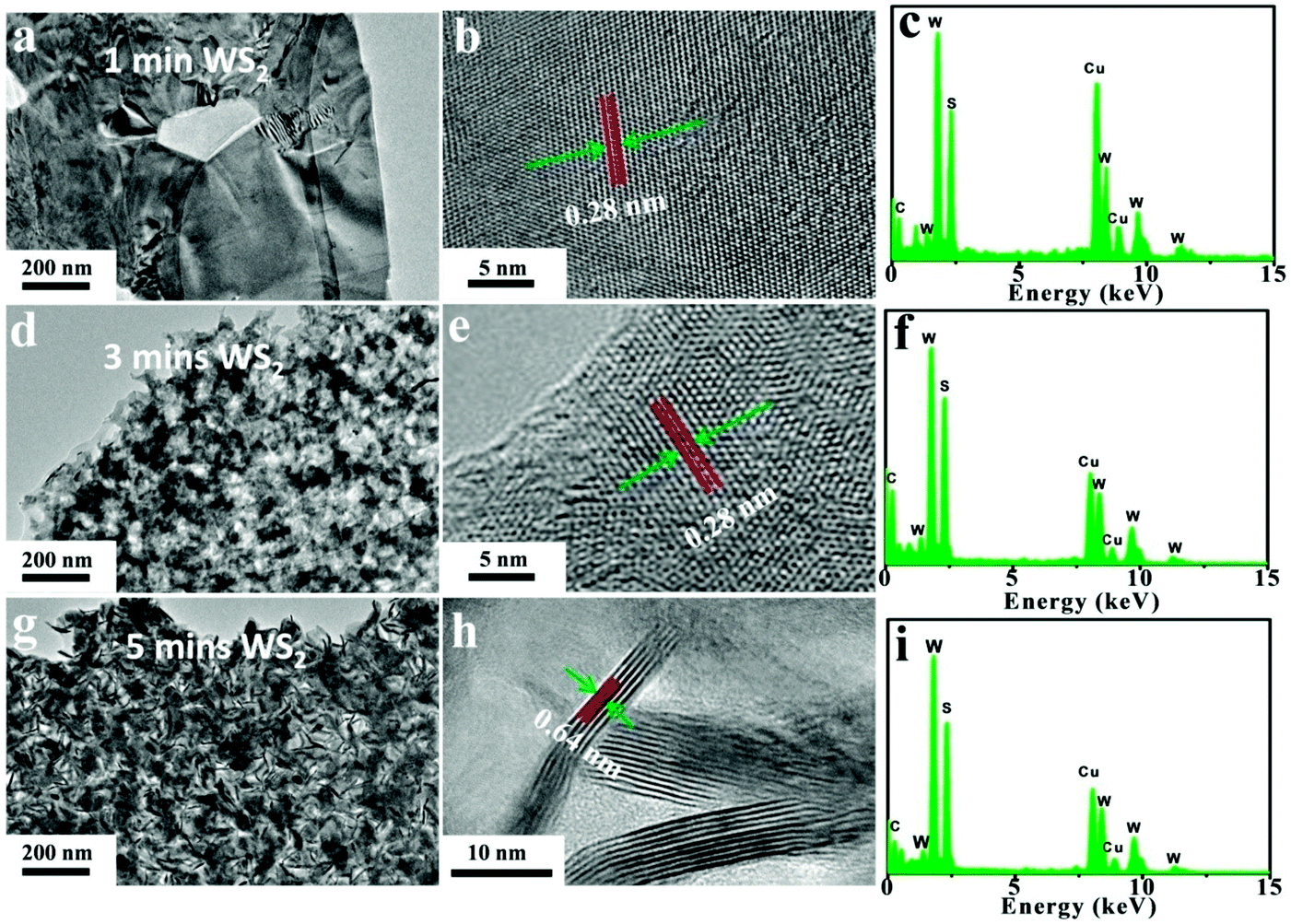 | ||
| Fig. 4 Transmission electron microscopy (TEM) images of 1 min, 3 min and 5 min WS2 films on carbon-coated copper fiber (a, d and g). Top view high-resolution transmission electron microscopy (HRTEM) images (b, e and h) of the vertically grown WS2 nanosheets and the horizontally grown nanosheets. The lattice spacing was approximately 0.64 and 0.28 nm for vertically and horizontally grown WS2 nanosheets, respectively. Energy-dispersive X-ray spectroscopy (EDS) spectra (c, f and i) of WS2 films fabricated with different sputtering times (a–c, 1 min, d–f, 3 min, g–i, 5 min). | ||
Cross-sectional TEM images of the three samples were taken for further investigation of the internal structure of the WS2 films and are shown in Fig. 5. The cross-sectional TEM images of WS2 films with different thicknesses are shown in Fig. 5(a–c). The WS2 films deposited with 1 min, 3 min and 5 min sputtering times had uniform thicknesses of approximately 11, 15, and 30 nm, and the numbers of layers estimated from the above cross-sectional TEM images were approximately 18–20, 15–17 and 8–10, respectively. When the sputtering time was increased from 1 min to 3 min, vertically grown nanosheets began to appear. In the sample fabricated with a 5 min deposition time, a large number of vertically grown nanosheets were clearly produced.
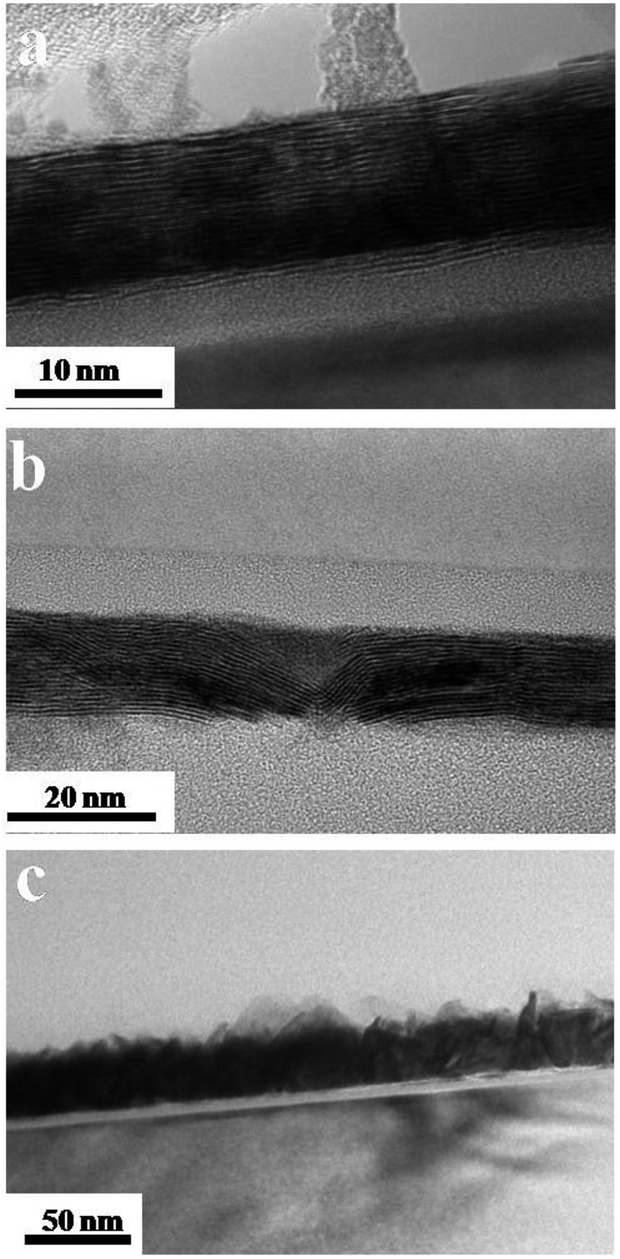 | ||
| Fig. 5 Cross-sectional HRTEM images of the WS2 films. (a) 1 min, (b) 3 min and (c) 5 min. | ||
To investigate the exciton dynamics of the few-layer WS2 films, the exciton radiative lifetime of a WS2 film was measured by using an 800 nm (100 fs) excitation laser source. Fig. 6 presents the decay curve for the 5 min WS2 film on a linear scale and a logarithmic scale. The decay curve clearly exhibits multi-exponential decay and can be well fitted using the triple exponential decay function A1e−t/τ1 + A2e−t/τ2 + A3e−t/τ3, where τ1 < τ2 < τ3; τi denotes the exponential decay lifetime of each component in the WS2 nanofilms; each pre-exponential factor Ai is the corresponding weight of the i'th component; and the subscript i is equal to 1, 2 or 3. The fitting decay time constants are τ1 = 512 ps (67.5% of weight), τ2 = 1311 ps (26.2% of weight) and τ3 = 2883 ps (6.3% of weight). Thus, the corresponding mean decay time (τm) of the WS2 film is 870.71 ps. This result is essentially consistent with the decay time of WS2 nanosheets (∼1 ns) presented in previous research works.60,61
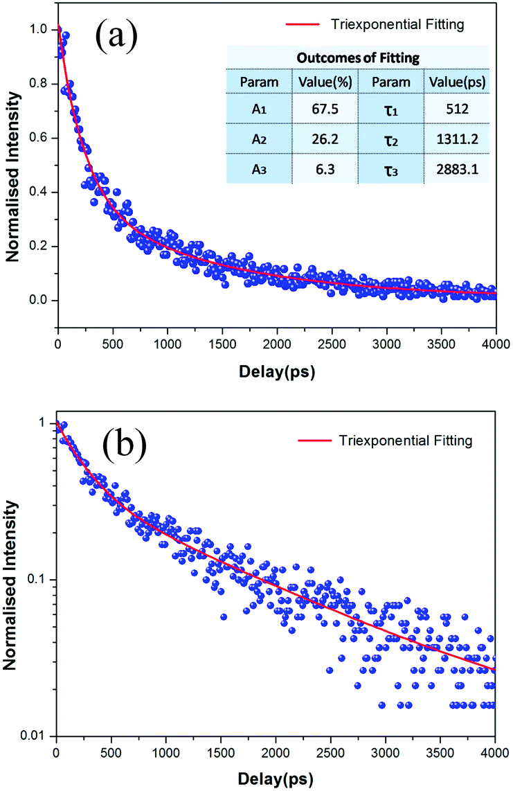 | ||
| Fig. 6 Exciton dynamics for 5 min WS2 film with a pump wavelength of 800 nm on a linear scale (a) and a logarithmic scale (b), revealing multi-exponential decay. The solid line is fitted using a triexponential decay function, and the outcomes of the fitting are presented in the inset table. | ||
3 Experimental results
Two sets of Z-scan experimental data are presented to examine the relationship between the nonlinear optical (NLO) properties of WS2 samples fabricated with different sputtering times (1 min, 3 min and 5 min) under condition (A), a constant pulse width (100 fs) but varying pump pulse energies (1 μJ, 1.5 μJ and 2 μJ), and condition (B), a constant pump pulse energy (2 μJ) but varying pulse durations (100 fs, 200 ps, 10 ps and 10 ns). The Ti-sapphire excitation laser source was operated at 800 nm for all the experiments. A schematic diagram of the experimental setup of the open aperture Z-scan is shown in the ESI:† Fig. S1. The Z-scan experimental data marked with squares, circles, triangles and rhombuses are shown in Fig. 7 and 8, and all the related theoretical fittings shown by solid lines were calculated by eqn (2).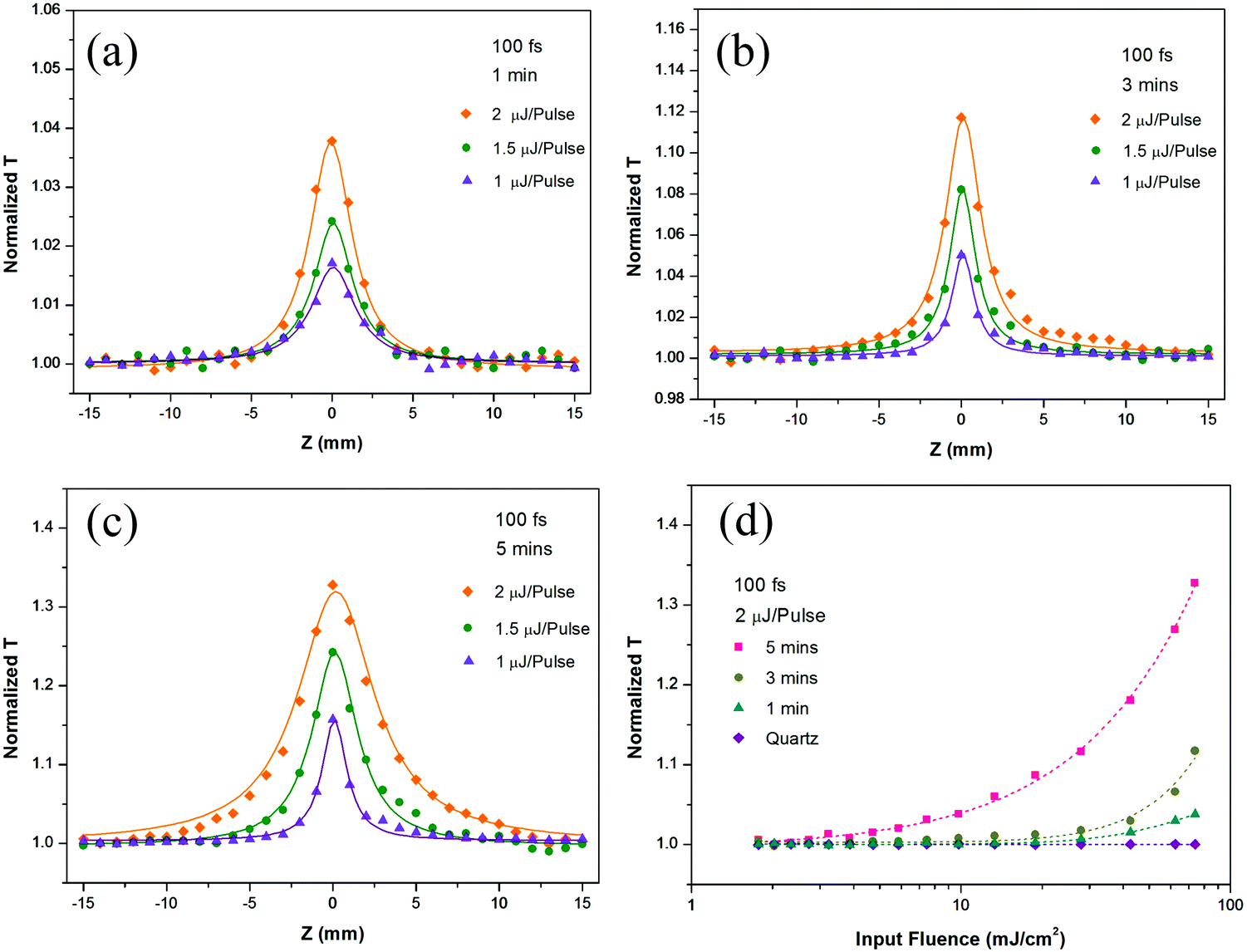 | ||
| Fig. 7 Open aperture Z-scan results for few-layer WS2 films fabricated with different magnetron sputtering times (a, 1 min; b, 3 min; c, 5 min) at a 100 fs (800 nm) laser pulse with different energies. (d) Normalized transmittance versus input fluence for 1 min, 3 min, and 5 min WS2 films and the pure quartz substrate under 2 μJ laser pulse excitation. | ||
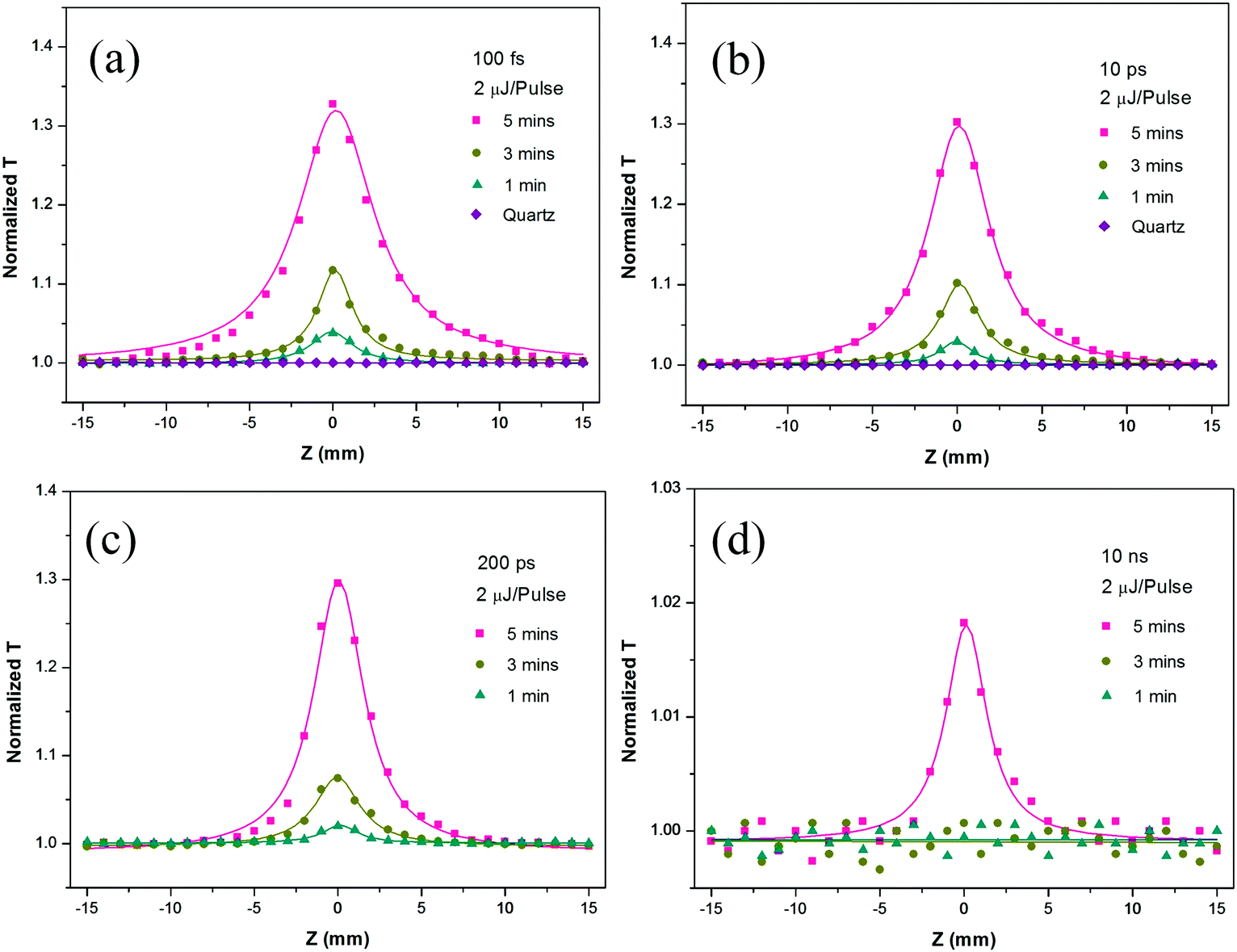 | ||
| Fig. 8 Z-scan results of 1 min, 3 min and 5 min WS2 films for (a) 100 fs, (b) 10 ps, (c) 200 ps and (d) 10 ns laser pulses at 800 nm. The response for the pure substrate is also included. | ||
3.1 Condition (A) a constant pulse width (100 fs) but various pump pulse energies (1 μJ, 1.5 μJ and 2 μJ)
Only SA was observed for all samples under excitation by a 100 fs pulse with various pulse energies, as shown in Fig. 7. The NLO effect grew stronger as the pulse energy increased. The measured normalized transmission increased to its maximum as the sample position approached the focus. The Z position shown in Fig. 7(a)–(c) can be translated into input fluence, which can be calculated by dividing the input pulse energy by the measured beam spot area at different Z positions. An example is given in Fig. 7(d), which shows the normalized transmission with respect to different input fluences under excitation by a 2 μJ 100 fs pulse. No NLO effect was observed from the quartz substrate alone. Therefore, the NLO properties were derived from the deposited WS2 materials. These results indicate that the 5 min sample with the larger pulse energy (2 μJ) exhibited the strongest SA properties among the various samples and excitation pulse energies. The observed results are reasonable, as the SA effect depends on the amount of nonlinear materials and the pulse energy. To ensure the NLO properties were not the results of nonlinear optical damage, the sample was examined under a microscope after each experiment. No laser damage was observed for all samples under excitation by a pulse energy of 2 μJ.3.2 Condition (B) the same pump pulse energy (2 μJ) but various pulse duration (100 fs, 200 ps, 10 ps and 10 ns)
This section presents the experimental data for various WS2 film samples under excitation by the same pulse energy 2 μJ with different pulse widths. This information will give us a deeper understanding of the NLO properties of these materials changes with respect to pulse width modulation.As shown in Fig. 7 and 8, all the samples exhibited a prominent ultrafast SA response or no NLO response. The SA behaviors observed for the three WS2 films implied that their band gap energies were all smaller than 1.55 eV (the one-photon energy of the 800 nm exciting laser). The band gap of the few-layer WS2 films was approximately 1.3 eV based on the previous reports.33,62,63 Therefore, the NLO effects of the three WS2 nanofilms can be attributed to the strong single photon absorption and Pauli blocking in semiconductor materials.64
4 Nonlinear absorption model and discussion
The following nonlinear absorption model was widely used to fit all the Z-scan data and to quantitatively analyze the corresponding NLO coefficients:65,66| α(I) = α0 − αNLI | (1) |
 | (2) |
| Sample | 800 nm laser | T L (%) | α 0 (cm−1) | α NL (cm GW−1) | I S (GW cm−2) | F on (mJ cm−2) | ΔT (%) |
|---|---|---|---|---|---|---|---|
| 1 min WS2 | 100 fs | 94.84 | 6.97 × 10⁴ | 97.55 ± 8.83 | 306.16 ± 25.41 | 18.86 | 3.8 |
| 10 ps | (9.63 ± 0.18) × 103 | 3.1 ± 0.06 | 27.9 | 2.9 | |||
| 200 ps | (1.66 ± 0.33) × 105 | 0.18 ± 0.03 | 42.5 | 1.9 | |||
| 3 min WS2 | 100 fs | 79.25 | 1.58 × 10⁵ | 162.96 ± 15.70 | 455.07 ± 39.99 | 7.47 | 11.7 |
| 10 ps | (1.67 ± 0.02) × 104 | 4.45 ± 0.05 | 9.8 | 10.2 | |||
| 200 ps | (2.77 ± 0.40) × 105 | 0.27 ± 0.03 | 13.32 | 7.4 | |||
| 5 min WS2 | 100 fs | 60.97 | 1.91 × 10⁵ | 314.67 ± 5.43 | 282.63 ± 4.8 | 2.73 | 32.1 |
| 10 ps | (2.87 ± 0.01) × 104 | 3.09 ± 0.01 | 3.87 | 30.2 | |||
| 200 ps | (5.71 ± 0.40) × 105 | 0.16 ± 0.01 | 5.86 | 28.5 | |||
| 10 ns | (2.20 ± 0.42) × 106 | 0.04 ± 0.006 | 42.5 | 1.8 | |||
Table 1 shows that the linear transmittance, TL, decreases and the linear absorption coefficient, α0, increases with the sputtering time as more WS2 is deposited on the substrate. The value of αNL also increases with sputtering time. This result implies that the nonlinear absorption will increase with increasing deposition time. For instance, αNL of the 5 min film is approximately three times higher than that of the 1 min film for 100 fs, 10 ps and 200 ps pulses. However, Is of all the three WS2 films did not change greatly with respect to sputtering time but decreased rapidly for increasing pulse duration, e.g., Is of the 5 min sample decreased from 282.63 GW cm−2 for 100 fs to 0.16 GW cm−2 for 200 ps, which, to the best of our knowledge, is the lowest Is among TMDs in the ps region.29,66,68
The onset fluence (Fon) denotes the NLO onset threshold, defined as the input fluence point at which the normalized transmittance of SA materials begins to increase. The modulation depth (ΔT) is the maximum possible change in transmittance induced by incident laser pulses. Fon and ΔT are two important SA parameters which are widely used to evaluate the practical performance of saturable absorbers. In general, for a saturable absorber used in passive mode-locking or Q-switching lasers, a lower Fon means lower laser threshold for the onset of pulse operation and a larger ΔT leads to shorter pulse generation and more reliable self-starting of mode-locking.50–53 For easy comparison, the onset fluence Fon and modulation depth ΔT are plotted against the sputtering times of samples for different pulse width at the same excitation energy of 2 μJ in Fig. 9(a and b) respectively. As shown in Fig. 9 and Table 1, generally, as the magnetron sputtering time increased from 1 min to 5 min, the onset fluence Fon of the SA response dropped, and the modulation depth ΔT of SA increased. This indicates that Fon decreases and ΔT increases with increasing film thickness, decreasing numbers of layers, and increasing amount of vertically grown WS2 nanosheet. For various pulse duration, the key SA parameters, modulation depth ΔT and onset fluence Fon, have been demonstrated to be greatly modifiable by controlling the film thickness and structure via adjusting the magnetron sputtering time during the fabrication process.
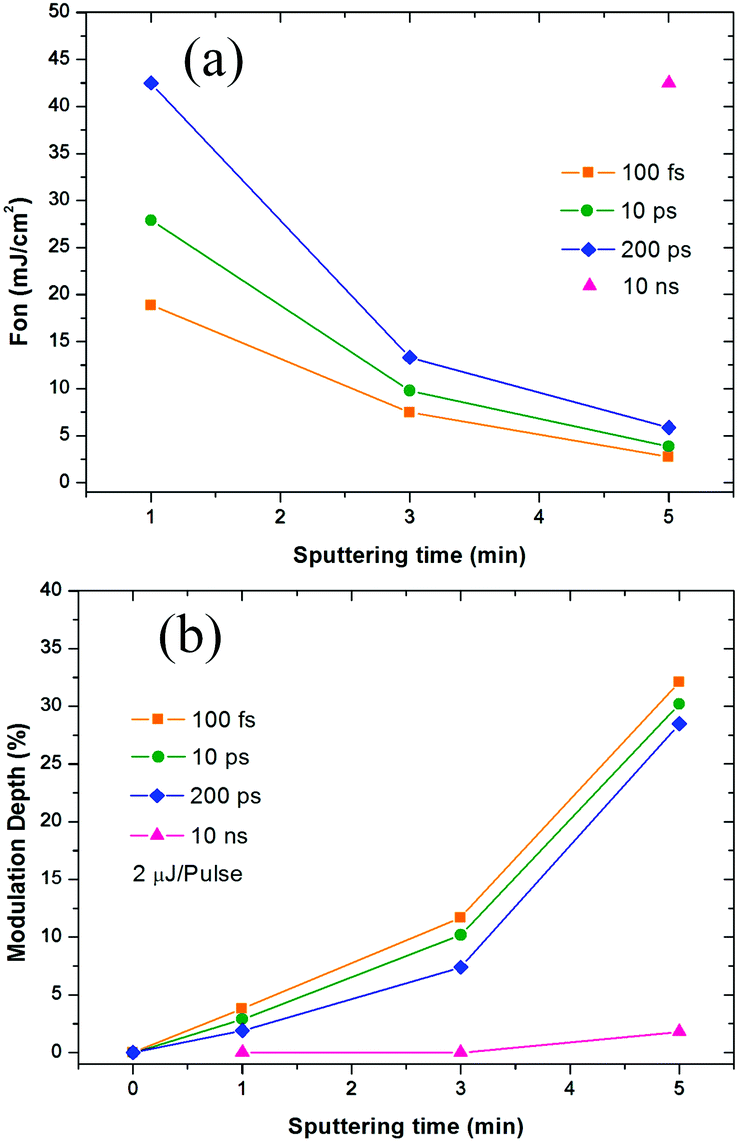 | ||
| Fig. 9 Onset fluence Fon (a) and modulation depth ΔT (b) of WS2 films fabricated with different sputtering times for 100 fs, 10 ps, 200 ps and 10 ns laser pulses (800 nm, 2 μJ). | ||
In this section, the modulation of Fon and ΔT by changing the sputtering time at various pulse widths will be discussed. Generally, the modulation of Fon and ΔT is quite large: (1) Fon was reduced by ∼86% for all three pulse durations (100 fs, 10 ps and 200 ps). (2) The value of ΔT was also greatly enhanced by 840%, 1040% and 1500% for 100 fs, 10 ps and 200 ps pulses. These enhancements were achieved by increasing the sputtering time from 1 min to 5 min. Therefore, we can conclude that the values of Fon and ΔT can be modified greatly by changing the sputtering time. Compared with other WS2 films used in previous studies under the same excitation wavelength and duration of 800 nm and 100 fs, respectively, the WS2 films used in this work exhibited larger modulation depth ΔT. With a similar value of TL ≈ 95%, the ΔT value obtained for the 1 min sample was 3.8%, which was approximately 50% larger than the previous record.67
Additionally, Fig. 9 and Table 1 reveal that the changes in Fon and ΔT with respect to the changing pulse width can also be quantified. Fon approximately doubled (∼100%) for all three samples as the pulse duration was changed from 100 fs to 200 ps (1000 times). The value of ΔT decreased by 50% for the 1 min, 36.7% for the 3 min and 11.2% for the 5 min sample as the pulse width increased from 100 fs to 200 ps. The reduction in ΔT was smaller for WS2 samples with longer sputtering times. Fig. 8(d) and 9 show weak SA for the 5 min sample under the excitation of a 10 ns pulse and no SA for the other two samples. For this reason, only a single data point for the 10 ns pulse is shown in Fig. 9(a and b). Overall, the WS2 films prepared for this work possess prominent ultrafast SA parameters in both the fs and ps regions and can fully satisfy various ultrafast SA device applications, including passive mode-lockers, passive Q-switchers, optical switches, etc. These results confirm that the 5 min sample offers the strongest NLO properties, and therefore, Fig. 10(a–c) were plotted for the detailed comparison of various pulse widths.
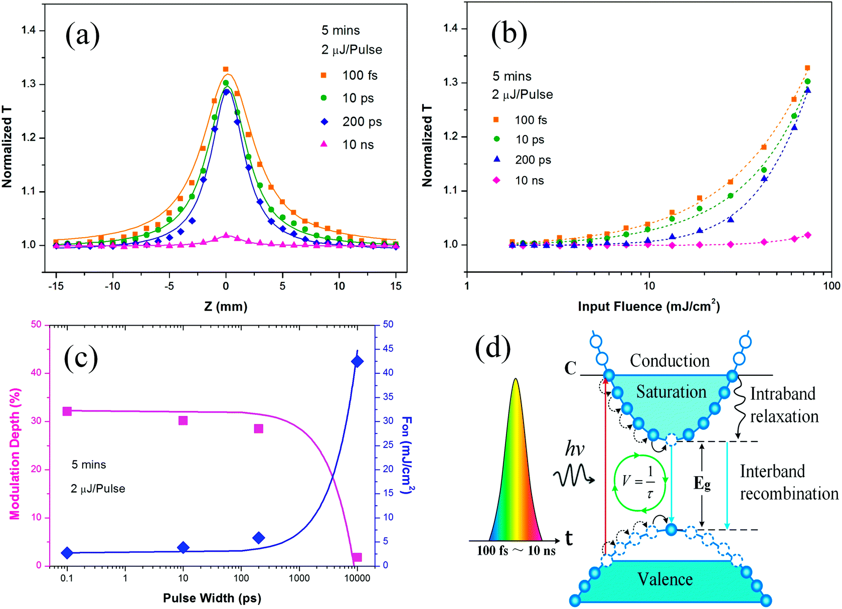 | ||
| Fig. 10 Comparison of SA responses (normalized transmittance versus Z position (a) and input fluence (b)) of the 5 min WS2 film for 100 fs, 10 ps, 200 ps and 10 ns laser pulses with 2 μJ energy. (c) Corresponding SA modulation depth ΔT and onset fluence Fon as a function of excitation pulse width. The solid curves were plotted to show the conclusions of our theoretical model. Square – modulation depth; diamond – Fon. (d) Schematic of SA and relaxation processes in WS2 film excited by ultrashort laser pulses. | ||
Fig. 10 summarizes the SA responses of the 5 min sample. The SA of the sample decayed slowly when the pulse width increased from fs to ps but was sharply weakened by the ns pulse excitation, as shown in Fig. 10(a)–(c). The corresponding pulse width dependences of the SA modulation depth ΔT and the onset fluence Fon are shown in Fig. 10(c). Fig. 10(c) shows that ΔT decreased and Fon increased slowly when the pulse width was increased from 100 fs to 200 ps. However, the changes accelerated as the pulse width increased further from 200 ps to 10 ns. Fon increased dramatically from 5.86 mJ cm−2 to 42.5 mJ cm−2 (725%) as the pulse duration changed from 200 ps to 10 ns. A dramatic reduction from 28.5% to 1.8% (1583%) in ΔT of the 5 min WS2 sample occurred as the pulse duration changed from 200 ps to 10 ns. Notably, as the duration of the laser pulses increased from 100 fs to 200 ps, the peak power of the laser pulses decreased by 2000 times, but the values of ΔT and Fon showed no obvious changes. As far as we know, no interpretation or theoretical analysis of this phenomenon exists. The mechanism by which the SA parameters of such TMDs varied with the pulse width thus far remains unclear.
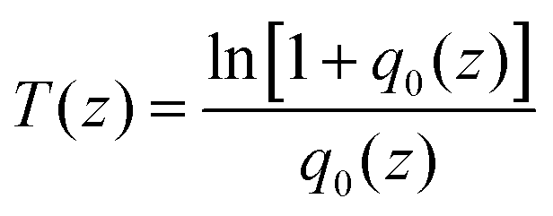
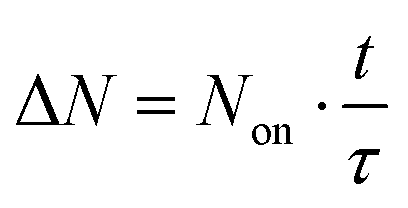
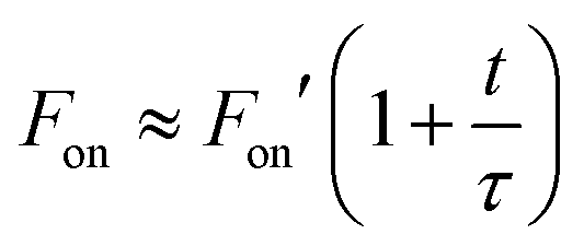
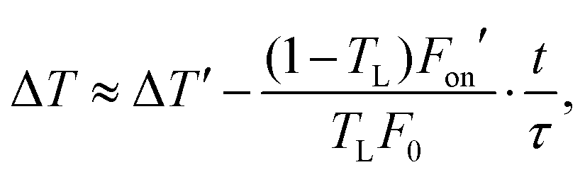
In this section, a pulse width-dependent SA theoretical model that considers the effects of the interband exciton recombination is first proposed to understand and analyze the mechanism by which the SA properties of WS2 vary with the excitation pulse width. Then, two analytical expressions for the key SA parameters (Fon and ΔT) in term of pulse width are deduced by using the energy band theory and exciton dynamics of the WS2 nanofilms. As shown in Fig. 10(d), a large number of free carriers are excited from the valence band to level C of the conduction band. These photoexcited electrons consequently decay to lower energy levels by intraband relaxation (<500 fs).60,72 When the input fluence is greater than or equal to the SA onset fluence Fon, the states below the energy level C in the conduction band are fully filled. Then, further absorption is blocked (i.e., Pauli-blocking), and saturated absorption occurs.73 Interband charge recombination has usually been ignored in previous research works.29,67,68 In fact, the excitons at the bottom of the conduction band relax by interband recombination at the speed 1/τ, where τ is the exciton radiative decay lifetime of the material. However, within the pump pulse duration, the decayed electrons reabsorb another photon and jump back into the conduction band to refill the unfilled states. This process is dynamic. The ratio between pulse duration, t, and the exciton radiative decay lifetime plays a critical role in SA properties. The exciton radiative decay is generally believed to be negligible if it is much longer than the pump pulse duration. However, as mentioned previously, decay will always occur even within the exciton decay lifetime. Based on our experimental data shown in Table 1, even within the decay lifetime (∼0.87 ns), a longer excitation pump pulse (200 ps) will still exhibit a higher Fon than that of 100 fs, although by only 2 times. However, if the pulse width is much longer than the decay lifetime, Fon is expected to become much higher as the exciton decay becomes more significant. Thus, if the sample is pumped within its lifetime, energy can be efficiently absorbed for the SA effect. The duration of the 10 ns pulse is much longer than the WS2 decay lifetime, which implies that the decay of excited electrons becomes significant and that, therefore, more pumping energy is needed to saturate the sample. Accordingly, the following new theoretical model based on the ratio of t and τ was developed to account for interband recombination.
During this process, the maximum excited state population, Non, was kept constant, and then the total number of the recombination excitons, ΔN, could be calculated by
 | (3) |
 | (4) |
 | (5) |
5 Conclusions
In summary, large-area samples of WS2 nanofilms with different thicknesses and morphologies deposited on quartz were fabricated by magnetron sputtering for various deposition times. The 1 min and 3 min WS2 films contained mainly horizontally grown WS2, while the 5 min films contained many vertically grown few-layered WS2 nanosheets. The characteristics and the ultrafast NLO properties of these nanofilms were investigated systematically by Z-scan. The WS2 films were found to possess prominent ultrafast SA properties under excitation by an 800 nm pulsed laser with energy up to 2 μJ and varying pulse durations in the fs, ps and ns regions. Some key SA parameters, e.g., the onset fluence Fon and the modulation depth ΔT, can be greatly modified by adjusting the thickness and morphology via controlling the magnetron sputtering time. A pulse width-dependent SA model that considers the effects of interband exciton recombination was proposed for the first time. The ratio between the decay lifetime and pulse width is critical for the SA effect. Laser pulses with the same pulse energy but a duration shorter than the decay lifetime produce a stronger SA effect. Two analytical expressions for the variation of the onset fluence Fon and the modulation depth ΔT with the excitation laser pulse width are derived. Our experimental results were in good agreement with the analytical predictions. These expressions can be employed to calculate the values of Fon and ΔT for various pulse widths for the TMD materials and further develop various ultrafast lasers and nanosecond lasers. These research findings have great value for both basic science and practical applications.Conflicts of interest
There are no conflicts to declare.Acknowledgements
We would like to thank Associate Professor Wei Zheng from the Shenzhen Institutes of Advanced Technology, Chinese Academy of Sciences for measuring the decay lifetimes of the WS2 nanofilms. This work is financially supported by the Shenzhen-Hong Kong Innovation Cooperation Project (Grant No. SGLH20150205162842428), Hong Kong Innovation and technology fund under Grant GHP/007/14SZ, the Research Grants Council of Hong Kong, China (Project Number: GRF 152109/16E PolyU B-Q52T), the Science and Technology Innovation Commission of Shenzhen (JCYJ20170412111625378, JCYJ20170302153540973 and GRCK2017042110412823), the National Special Foundation of China for Major Science Instrument (61227802) and Hong Kong Polytechnic University (Project number: G-YBFR).Notes and references
- F. Xia, H. Wang, D. Xiao, M. Dubey and A. Ramasubramaniam, Nat. Photonics, 2014, 8, 899–907 CrossRef CAS
.
- A. K. Geim, Nat. Mater., 2007, 6, 183–190 CrossRef CAS PubMed
- A. K. Geim, Science, 2009, 324, 1530–1534 CrossRef CAS PubMed
- L. H. Zeng, M. Z. Wang, H. Hu, B. Nie, Y. Q. Yu, C. Y. Wu, L. Wang, J. G. Hu, C. Xie and F. X. Liang, ACS Appl. Mater. Interfaces, 2013, 5, 9362–9366 CAS
- L. Zeng, C. Xie, L. Tao, H. Long, C. Tang, Y. H. Tsang and J. Jie, Opt. Express, 2015, 23, 4839–4846 CrossRef CAS PubMed
- B. Nie, J. G. Hu, L. B. Luo, C. Xie, L. H. Zeng, P. Lv, F. Z. Li, J. S. Jie, M. Feng and C. Y. Wu, Small, 2013, 9, 2872–2879 CrossRef CAS PubMed
- W. Y. Kong, G. A. Wu, K. Y. Wang, T. F. Zhang, Y. F. Zou, D. D. Wang and L. B. Luo, Adv. Mater., 2016, 28, 10725–10731 CrossRef CAS PubMed
- L. B. Luo, J. J. Chen, M. Z. Wang, H. Hu, C. Y. Wu, Q. Li, L. Wang, J. A. Huang and F. X. Liang, Adv. Funct. Mater., 2014, 24, 2794–2800 CrossRef CAS
- Y. Ye, G. Lin, L. Dai, M. Hu, W. Feng, D. Yu, Z. Shi, B. Yu, X. Guo and G. Qin, J. Mater. Chem., 2011, 21, 11760–11763 RSC
- Y. M. Lin, C. Dimitrakopoulos, K. A. Jenkins, D. B. Farmer, H. Y. Chiu, A. Grill and P. Avouris, Science, 2010, 327, 662 CrossRef CAS PubMed
- Z. Li, W. Xu, Y. Yu, H. Du, K. Zhen, J. Wang, L. Luo, H. Qiu and X. Yang, J. Mater. Chem. C, 2015, 4, 362–370 RSC
- L. B. Luo, C. Xie, X. H. Wang, Y. Q. Yu, C. Y. Wu, H. Hu, K. Y. Zhou, X. W. Zhang and J. S. Jie, Nano Energy, 2014, 9, 112–120 CrossRef CAS
- C. Meng, S. L. Yu, H. Q. Wang, Y. Cao, L. M. Tong, W. T. Liu and Y. R. Shen, Light: Sci. Appl., 2015, 4, e348 CrossRef CAS
- Y. Wang, Z. S. Qu, J. Liu and Y. H. Tsang, J. Light Technol., 2012, 30, 3259–3262 CrossRef CAS
- D. Jariwala, T. J. Marks and M. C. Hersam, Nat. Mater., 2017, 16, 170 CrossRef CAS PubMed
- J. Yang, R. Xu, J. Pei, W. M. Ye, F. Wang, Z. Wang, S. Zhang, Z. Yu and Y. Lu, Light: Sci. Appl., 2015, 4, e312 CrossRef CAS
- J. Xiao, Z. Ye, Y. Wang, H. Zhu, Y. Wang and X. Zhang, Light: Sci. Appl., 2015, 4, 366 CrossRef
- L. Zhu, F. Liu, H. Lin, J. Hu, Z. Yu, X. Wang and S. Fan, Light: Sci. Appl., 2016, 5, e16052 CrossRef CAS
- K. F. Mak and J. Shan, Nat. Photonics, 2016, 10, 216–226 CrossRef CAS
- Y. Shi, H. Li and L. J. Li, Chem. Soc. Rev., 2015, 44, 2744–2756 RSC
- L. Zeng, L. Tao, C. Tang, B. Zhou, H. Long, Y. Chai, S. P. Lau and Y. H. Tsang, Sci. Rep., 2016, 6, 20343 CrossRef CAS PubMed
- M. L. Tsai, S. H. Su, J. K. Chang, D. S. Tsai, C. H. Chen, C. Wu, L. J. Li, L. J. Chen and J. H. He, ACS Nano, 2014, 8, 8317 CrossRef CAS PubMed
- L. H. Zeng, S. H. Lin, Z. J. Li, Z. X. Zhang, T. F. Zhang, C. Xie, C. H. Mak, Y. Chai, S. P. Lau, L. B. Luo and Y. H. Tsang, Adv. Funct. Mater., 2018 DOI:10.1002/adfm.201705970
- H. Long, L. Tao, C. Y. Tang, B. Zhou, Y. Zhao, L. Zeng, S. F. Yu, S. P. Lau, Y. Chai and Y. H. Tsang, Nanoscale, 2015, 7, 17771–17777 RSC
- L. Tao, H. Long, B. Zhou, S. F. Yu, S. P. Lau, Y. Chai, K. H. Fung, Y. H. Tsang, J. Yao and D. Xu, Nanoscale, 2014, 6, 9713–9719 RSC
- H. Long, L. Tao, C. Y. Tang, H. Y. Tam, Q. Wen and Y. H. Tsang, J. Mater. Chem. C, 2016, 4, 678–683 RSC
- C. Chen, W. Yu, T. Liu, S. Cao and Y. Tsang, Sol. Energy Mater. Sol. Cells, 2017, 160, 43–53 CrossRef CAS
- J. Zhou, S. Dai, W. Dong, X. Su, L. Fang, F. Zheng, X. Wang and M. Shen, Appl. Phys. Lett., 2016, 109, 332 Search PubMed
- K. Wang, J. Wang, J. Fan, M. Lotya, A. O'Neill, D. Fox, Y. Feng, X. Zhang, B. Jiang and Q. Zhao, ACS Nano, 2013, 7, 9260 CrossRef CAS PubMed
- W. Shuxian, Y. Haohai, Z. Huaijin, W. Aizhu, Z. Mingwen, C. Yanxue, M. Liangmo and W. Jiyang, Adv. Mater., 2014, 26, 3538 CrossRef PubMed
- H. Zhang, S. B. Lu, J. Zheng, J. Du, S. C. Wen, D. Y. Tang and K. P. Loh, Opt. Express, 2014, 22, 7249–7260 CrossRef CAS PubMed
- K. Wu, X. Zhang, J. Wang, X. Li and J. Chen, Opt. Express, 2015, 23, 11453–11461 CrossRef CAS PubMed
- W. Zhao, Z. Ghorannevis, L. Chu, M. Toh, C. Kloc, P. H. Tan and G. Eda, ACS Nano, 2012, 7, 791–797 CrossRef PubMed
- C. Y. Tang, P. K. Cheng, L. Tao, H. Long, L. H. Zeng, Q. Wen and Y. H. Tsang, J. Light Technol., 2017, 1 Search PubMed
- P. Yan, H. Chen, A. Liu, K. Li, S. Ruan, J. Ding, X. Qiu and T. Guo, IEEE J. Sel. Top. Quantum Electron., 2016, 23, 33–38 CrossRef
- Y. Cheng, J. Peng, B. Xu, H. Yang, Z. Luo, H. Xu, Z. Cai and J. Weng, IEEE Photonics J., 2017, 8, 1–6 Search PubMed
- Z. Luo, D. Wu, B. Xu, H. Xu, Z. Cai, J. Peng, J. Weng, S. Xu, C. Zhu and F. Wang, Nanoscale, 2016, 8, 1066 RSC
- W. Li, J. Peng, Y. Zhong, D. Wu, H. Lin, Y. Cheng, Z. Luo, J. Weng, H. Xu and Z. Cai, Opt. Mater. Express, 2016, 6, 2031–2039 CrossRef CAS
- M. Dong, Y. Wang, C. Ma, H. Lei, B. Jiang, X. Gan, S. Hua, W. Zhang, T. Mei and J. Zhao, Sci. Rep., 2015, 5, 7965 CrossRef PubMed
- C. Wei, H. Luo, H. Zhang, C. Li, J. Xie, J. Li and Y. Liu, Laser Phys. Lett., 2016, 13, 105108 CrossRef
- D. I. Yeom, H. Jeong, K. Oh, R. Khazaeinezhad, S. H. Kassani and T. Nazari, Opt. Mater. Express, 2015, 5, 373–379 CrossRef
- D. I. Yeom, H. Jeong, K. Oh, R. Khazaeinezhad and S. H. Kassani, J. Light Technol., 2015, 33, 3550–3557 CrossRef
- L. Pang, W. Liu, W. Tian, H. Han and Z. Wei, IEEE Photonics J., 2016, 8, 1–7 CrossRef
- K. Y. Lau, A. A. Latif, M. H. A. Bakar, F. D. Muhammad, M. F. Omar and M. A. Mahdi, Appl. Phys. B: Lasers Opt., 2017, 123, 221 CrossRef
- B. Chen, X. Zhang, K. Wu, H. Wang, J. Wang and J. Chen, Opt. Express, 2015, 23, 26723–26737 CrossRef CAS PubMed
- P. Yan, A. Liu, Y. Chen, J. Wang, S. Ruan, H. Chen and J. Ding, Sci. Rep., 2015, 5, 12587 CrossRef CAS PubMed
- B. Guo, Y. Yao, P. G. Yan, K. Xu, J. J. Liu, S. G. Wang and Y. Li, IEEE Photonics Technol. Lett., 2016, 28, 323–326 CrossRef CAS
- C. Lan, C. Li, H. Xia, H. Li, S. Zhang, X. Zhang and Y. Liu, Opt. Express, 2014, 22, 17341–17348 CrossRef PubMed
- A. Chernikov, C. Ruppert, H. M. Hill, A. F. Rigosi and T. F. Heinz, Nat. Photonics, 2015, 9, 466–470 CrossRef CAS
- F. X. Kurtner, J. A. D. Au and U. Keller, IEEE J. Sel. Top. Quantum Electron., 1998, 4, 159–168 CrossRef
- Q. W. Sheng, M. Feng, W. Xin, H. Guo, T. Y. Han, Y. G. Li, Y. G. Liu, F. Gao, F. Song and Z. B. Liu, Appl. Phys. Lett., 2014, 105, 666 Search PubMed
- J. Li, H. Luo, Z. Bo, R. Lu, Z. Guo, Z. Han and L. Yong, Sci. Rep., 2016, 6, 30361 CrossRef CAS PubMed
- C. Hönninger, R. Paschotta, F. Morier-Genoud, M. Moser and U. Keller, J. Opt. Soc. Am. B, 1999, 16, 46–53 CrossRef
- B. Zhu, X. Chen and X. Cui, Sci. Rep., 2015, 5, 9218 CrossRef PubMed
- W. Zhao, Z. Ghorannevis, K. K. Amara, J. R. Pang, M. Toh, X. Zhang, C. Kloc, P. H. Tan and G. Eda, Nanoscale, 2013, 5, 9677–9683 RSC
- A. Berkdemir, H. R. Gutiérrez, A. R. Botello-Méndez, N. Perea-López, A. L. Elías, C. I. Chia, B. Wang, V. H. Crespi, F. López-Urías and J. C. Charlier, Sci. Rep., 2013, 3, 1755 CrossRef
- H. Zeng, G. B. Liu, J. Dai, Y. Yan, B. Zhu, R. He, L. Xie, S. Xu, X. Chen and W. Yao, Sci. Rep., 2013, 3, 1608 CrossRef PubMed
- D. Kong, H. Wang, J. J. Cha, M. Pasta, K. J. Koski, J. Yao and Y. Cui, Nano Lett., 2013, 13, 1341 CrossRef CAS PubMed
- Y. Jung, J. Shen, Y. Liu, J. M. Woods, Y. Sun and J. J. Cha, Nano Lett., 2014, 14, 6842–6849 CrossRef CAS PubMed
- H. Shi, R. Yan, S. Bertolazzi, J. Brivio, B. Gao, A. Kis, D. Jena, H. G. Xing and L. Huang, ACS Nano, 2013, 7, 1072–1080 CrossRef CAS PubMed
- M. Palummo, M. Bernardi and J. C. Grossman, Nano Lett., 2015, 15, 2794 CrossRef CAS PubMed
- D. Braga, I. G. Lezama, H. Berger and A. F. Morpurgo, Nano Lett., 2012, 12, 5218 CrossRef CAS PubMed
- W. S. Yun, S. W. Han, S. C. Hong, I. G. Kim and J. D. Lee, Phys. Rev. B: Condens. Matter Mater. Phys., 2012, 85, 033305 CrossRef
- Q. Bao, Z. Han, W. Yu, Z. Ni, Y. Yan, Z. X. Shen, K. P. Loh and Y. T. Ding, Adv. Funct. Mater., 2009, 19, 3077–3083 CrossRef CAS
- M. Sheik-Bahae, A. A. Said, T.-H. Wei, D. J. Hagan and E. W. Van Stryland, IEEE J. Quantum Electron., 1990, 26, 760–769 CrossRef CAS
- M. Sheik-Bahae, A. A. Said and E. W. Van Stryland, Opt. Lett., 1989, 14, 955–957 CrossRef CAS PubMed
- S. Zhang, N. Dong, N. Mcevoy, M. O'Brien, S. Winters, N. C. Berner, C. Yim, Y. Li, X. Zhang and Z. Chen, ACS Nano, 2015, 9, 7142–7150 CrossRef CAS PubMed
- K. Wang, Y. Feng, C. Chang, J. Zhan, C. Wang, Q. Zhao, J. N. Coleman, L. Zhang, W. J. Blau and J. Wang, Nanoscale, 2014, 6, 10530–10535 RSC
- X. F. Jiang, L. Polavarapu, S. T. Neo, T. Venkatesan and Q. H. Xu, J. Phys. Chem. Lett., 2012, 3, 785 CrossRef CAS PubMed
- P. L. Huang, W. L. Chen, T. W. Peng, C. Y. Su, C. Y. Yeh and W. H. Cheng, IEEE Photonics Technol. Lett., 2015, 27, 1791–1794 CrossRef CAS
- S. Kumar, M. Anija, N. Kamaraju, K. S. Vasu, K. S. Subrahmanyam, A. K. Sood and C. N. R. Rao, Appl. Phys. Lett., 2009, 95, 183 Search PubMed
- J. Shah, Superlattices Microstruct., 1989, 6, 293–302 CrossRef CAS
- E. Garmire, IEEE J. Sel. Top. Quantum Electron., 2002, 6, 1094–1110 CrossRef
Footnotes |
| † Electronic supplementary information (ESI) available. See DOI: 10.1039/c8tc00498f |
| ‡ These authors contributed equally to this work. Both institutes contributed equally to this work. |
| This journal is © The Royal Society of Chemistry 2018 |