
 Open Access Article
 This Open Access Article is licensed under a
 Creative Commons Attribution 3.0 Unported Licence
Screen printed carbon CsPbBr3 solar cells with high open-circuit photovoltage†
Isabella
Poli
 *ab,
Jenny
Baker
c,
James
McGettrick
c,
Francesca
De Rossi
c,
Salvador
Eslava
db,
Trystan
Watson
c and
Petra J.
Cameron
*ab
*ab,
Jenny
Baker
c,
James
McGettrick
c,
Francesca
De Rossi
c,
Salvador
Eslava
db,
Trystan
Watson
c and
Petra J.
Cameron
*ab
aDepartment of Chemistry, University of Bath, Bath BA2 7AY, UK. E-mail: i.poli@bath.ac.uk; p.j.cameron@bath.ac.uk
bCentre for Sustainable Chemical Technologies, University of Bath, Bath BA2 7AY, UK
cSPECIFIC, Swansea University Bay Campus, Fabian Way, Swansea, SA1 8EN, UK
dDepartment of Chemical Engineering, University of Bath, Bath BA2 7AY, UK
First published on 13th September 2018
Abstract
Screen printed mesoporous carbon solar cells (mC-PSC) are a promising fully printable technology that does not require organic hole conductors, expensive metal contacts or vacuum processing. However, when infiltrated with the archetypal CH3NH3PbI3 perovskite, mC-PSCs show low voltage which limits their use in innovative applications such as indoor light harvesting. Here we investigate both planar (C-PSC) and mesoporous (mC-PSC) carbon cells, based on all-inorganic CsPbBr3. Pure CsPbBr3 is a yellow material with an orthorhombic crystal structure at room temperature and a 2.3 eV band gap, which is not ideal for solar cell applications. However, CsPbBr3 is thermally stable up to over 400 °C and high-voltage planar carbon solar cells, with open circuit voltages of up to 1.29 V and efficiencies up to 6.7% have been reported in the literature. We focus on the effect of the post-annealing temperature on the material properties and photovoltaic activity. XPS and XRD results show a non-linear trend with temperature, with significant improvements in composition between 200 and 300 °C. Both the mesoporous and planar champion devices were obtained after heat processing at 400 °C, reaching PCEs of 8.2% and 5.7% respectively. The average Voc for the planar and mesoporous devices were 1.33 V and 1.27 V respectively with a record 1.44 V for the best mC-PSC.
Introduction
The photovoltaic (PV) market is currently dominated by crystalline silicon (c-Si). The price of c-Si modules has fallen recently, providing cost-competitive power compared to that delivered by fossil fuel technologies.1 High power conversion efficiencies (PCE), high stability and low-cost are therefore necessary for any new technology that wants to break into the PV market. Halide perovskites emerged as promising new PV material in 2012.2,3 Perovskite solar cells (PSCs) are composed of Earth-abundant elements and they can be deposited by low-temperature and inexpensive solution-based methods. Most importantly, PCEs have increased to a certified 23.3% in just few years.4Devices with record-efficiency use Au as back contact together with organic conductive polymers acting as hole transport material (HTM). Such architecture strongly limits the long-term stability of perovskite solar cells. Gold migration through the HTM into the perovskite material occurs when PSCs are exposed to high temperatures, irreversibly degrading the layers.5 Moreover, expensive pure Au is required, dominating the PSCs manufacturing costs.6 A widely used hole conducting polymer is spiro-OMeTAD (‘spiro’). Large-scale production of this material is prohibitive because it requires many synthetic and purification steps and uses expensive catalysts.7 Moreover, spiro is not highly conducting and additives, such as Li salts, are needed to achieve good device performance.8 The hygroscopic nature of such additives accelerates the degradation of PSCs.9 In order to reduce the detrimental effect of using Li salts, PTTA (poly[bis(4-phenyl) (2,4,6-trimethylphenyl)-amine]) was found as an efficient alternative HTM.10 However PTTA can still cause infiltration problems, as well as increase the fabrication cost.11
Solar cells without an organic hole conductor and gold as metal contact have been successfully synthesised.11,12 PSCs where the contact is a screen printed carbon layer have recently gained wide interest. In the case of mesoporous carbon devices, the perovskite is infiltrated into a 6–10 μm mesoporous carbon layer. This architecture was first demonstrated in 2013 (ref. 13) using methylammonium lead triiodide (MAPI) and very rapidly developed to a certified PCE of 15.6%.14–20 5-Ammoniumvaleric acid iodide (5-AVAI) can be used as an additive to obtain better pore filling and lower defect concentration.14,21 The highest PCEs of 15.6% were achieved by adding ammonium chloride (NH4Cl) to enable perovskite crystals with preferential growth orientation20 and replacing the most widely used 5-AVAI with a bifunctional conjugated organic molecule 4-(aminomethyl) benzoic acid hydroiodide.19 Printable solar cells with PCEs as high as 17% were also reported by using triple cation perovskite TiO2/Al2O3/NiO layered framework and carbon counter electrode.22 Advantages of carbon-based PSCs include good stability, due to the hydrophobic nature of carbon, and a low-cost scalable deposition process compatible with fast printing production.16,23 Recently, near infrared processing was investigated to further improve the commerciability of the technology by reducing the processing time and allowing the preparation of larger area modules.24 Infiltration of active materials onto large area carbon surfaces has been demonstrated using a mechanical dispenser and mesh25 and modules up to 198 cm2 in size have been reported.26 One disadvantage of mesoporous carbon cells is that the photovoltage measured in this architecture is still notably low. The highest open circuit voltage reported to date is 1.05 V.17 In contrast perovskite cells with an organic hole conductor can have open circuit voltages up to 1.4 V.27 It is therefore crucial to optimise carbon cells to improve the open circuit voltage. High voltage solar cells are essential for a variety of applications, such as charging low-power electronic batteries,28 indoor applications and photoelectrochemical unassisted water splitting.29
Most perovskite devices use methylammonium (MA) and formamidinium (FA) as organic cations. Another limitation in the commercialisation of organo-lead halide perovskites is their thermal and moisture instability. MA and FA are not stable in high humidity ambient conditions and at high temperature, requiring environmental controls during processing and encapsulation later.23 The most efficient perovskite devices use multi cation materials where organic FA and MA are mixed with the smaller inorganic cation Cs.30 All inorganic CsPbI3 has a black delta phase and PCEs of 10% have been reported.31 However, the material tends to form a wide bandgap non-perovskite phase at room temperature.32 The band gap and phase can be tuned by adding bromide to CsPbI3. The highest reported efficiency in literature on Cs-based perovskite devices with mixed halide is 14.6%;33 however at certain I![[thin space (1/6-em)]](https://www.rsc.org/images/entities/char_2009.gif) :Br ratios the material is unstable and separates into iodide rich and bromide rich regions under illumination.31,34
:Br ratios the material is unstable and separates into iodide rich and bromide rich regions under illumination.31,34
All-inorganic CsPbBr3 perovskites have recently attracted attention due to their high thermal stability. Thermogravimetric analysis (TGA) of CsPbBr3 performed under N2 flow showed a decomposition onset at about 580 °C and solar cells with mesoporous TiO2 as electron transport material ETM, spiro as HTM and Au as metal contact based on this material showed PCE of 6.2%.35,36 Very recently CsPbBr3 was also deposited using a dual-source vacuum evaporation technique achieving a PCE of 6.95%.37 CsPbBr3 crystallises in the orthorombic space group at room temperature; transitions to the tetragonal and then the cubic phase occur at 88 °C and 130 °C respectively.38 CsPbBr3 has been recently used in carbon-based architectures as well, showing no performance degradation over 3 months in humid air.39 Carbon cells with the architecture FTO/c-TiO2/m-TiO2/CsPbBr3/C (c: compact, m: mesoporous) achieved PCEs ranging between 5% and 6.7%.39–41 In these reports the CsPbBr3 films were annealed at 250 °C and the carbon layer was either screen printed or deposited by doctor blade technique. The highest voltage measured using this architecture was 1.29 V.40 Recently it was shown that by adding carbon and red phosphorus quantum dots at the TiO2/CsPbBr3 and CsPbBr3/C interfaces, improvements in the Voc up to 1.47 V could be achieved, with the highest PCE measured to be 8.2%.42,43
In this work, we report for the first time the preparation of mesoporous carbon CsPbBr3 solar cells (mC-PSC). The mC-PSC architecture consists of c-TiO2/m-TiO2/m-ZrO2/m-carbon with CsPbBr3 infiltrated through the stack. We compare this mC-PSC to planar c-TiO2/CsPbBr3/m-carbon (C-PSC). CsPbBr3 solar cells with carbon as top contact (C-PSC) have been previously reported in literature. In contrast, the preparation of mC-PSC by infiltration of CsPbBr3 into printable solar cells has not. Cell preparation was carried out under ambient atmosphere and the effect of post-annealing treatment with temperatures ranging between 200 and 400 °C was studied. When annealed at 400 °C enlarged crystal grains and complete conversion of precursor materials to CsPbBr3 was obtained. Our champion mC-PSC and C-PSC reached a PCE of 8.2% and 5.7%, respectively. Most importantly, an extremely high Voc of 1.44 V was achieved for mC-PSC, with an average of 1.27 V over 20 devices. As far as we know, this is the highest voltage ever seen using the c-TiO2/m-TiO2/m-ZrO2/m-carbon structure-based cell, which is notable for its low voltage. In C-PSC the CsPbBr3 crystal size is not constrained by the mesoporous carbon material, allowing free growing of the grains leading to a champion Voc of 1.45 V, with an open circuit voltage of 1.33 V averaged over 40 devices.
Experimental
Schematics of the fabrication process of mC-PSC and C-PSC are shown in Fig. 1.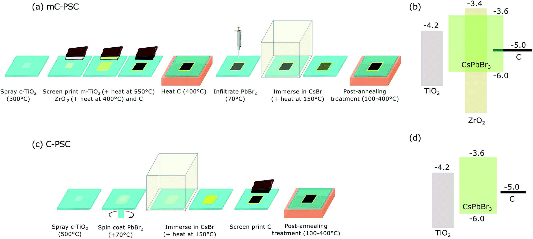 | ||
| Fig. 1 (a–c) Schematic showing the fabrication of a mesoporous carbon solar cell (mC-PSC) and a planar carbon solar cell (C-PSC). The temperatures within brackets indicate the deposition, sintering and annealing temperatures. The detailed fabrication process is explained in the experimental section; (b and c) energy band diagram of mC-PSC and C-PSC allowing a semiquantitative comparison of the two architectures. Band edge positions of the materials were taken from previous literature data.13,44 | ||
mC-PSC fabrication
TEC 7 fluorine doped tin oxide (FTO) glass substrates were etched using a Rofin Nd:YVO4 laser (532 nm) at a speed of 150 nm s−1. Substrates were cleaned with isopropanol (IPA, Sigma-Aldrich) and deionised (DI) water and further treated with O2 plasma. A compact layer of TiO2 was deposited via spray pyrolysis at 300 °C from a solution 1:9 of titanium di-isopropoxide bis(acetylacetonate) (Sigma) in IPA. 30 NRD TiO2 paste (Dyesol) 2:3 terpineol (Sigma) by weight was screen printed onto the c-TiO2 and cells were sintered at 550 °C for 30 min. ZrO2 paste (Solaronix) was screen printed on top of TiO2 and sintered at 400 °C for 30 min. A carbon paste (Gwent Electronic Materials) was screen printed on top of the ZrO2 and sintered at 400 °C for 30 min. 1 M of PbBr2 (98%, Sigma-Aldrich) was dissolved in N,N-dimethylformamide (DMF, anhydrous, Sigma-Aldrich) at 70 °C and 6 μl dropped onto the active area of each cell while substrates were heated at 70 °C and further sintered at 70 °C for 30 min. The cell was then immersed in CsBr (99.999%, Sigma-Aldrich) solution in methanol (17 mg ml−1 kept at 50 °C in a vertical staining jar). After 30 min immersion, the sample was annealed at 150 °C for 30 min. Devices were further post-annealed at different temperatures ranging between 100 and 400 °C for 30 min.
C-PSC fabrication
FTO glass (TEC 7) (Sigma-Aldrich) was etched with zinc powder and HCl. It was then cleaned in 2 vol% Hellmanex solution in water, followed by DI water, acetone (VWR), IPA (VWR) and ethanol (VWR) before being treated with UV-ozone cleaning. A compact TiO2 (c-TiO2) layer was deposited by spray pyrolysis, using a hand held atomiser to spray 20 mM solution of titanium diisopropoxide bis(acetylacetonate) (75 wt%, Sigma-aldrich) in IPA onto the substrates held at 500 °C. Substrates were then annealed at this temperature for 10 minutes. PbBr2 solution was spin coated on top of the substrates held at 70 °C at 2500 rpm for 30 s and each cell was further sintered at 70 °C for 30 min. The cell was then immersed in the CsBr solution kept at 50 °C in a vertical staining jar for 30 min before being annealed at 150 °C for 30 min. A carbon layer was deposited as top contact by doctor blading the carbon paste on top of the CsPbBr3 film. Devices were further post-annealed at different temperatures ranging between 100 and 400 °C for 30 min.Characterisation
Results and discussion
CsPbBr3 thin films were prepared in air using a 2-step method. PbBr2 was first deposited, then converted to CsPbBr3 by dipping into a CsBr solution, followed by annealing at 150 °C. The precursor films of PbBr2 appeared transparent; the colour of the films changed to bright yellow during the conversion in the CsBr solution. In order to promote the conversion of PbBr2 and CsBr to CsPbBr3, films were post annealed at temperatures between 100 and 400 °C. The morphology, structural properties and surface chemistry were analysed as a function of the processing temperature.TGA analysis of CsPbBr3 films performed under N2 flow previously reported in literature showed a decomposition onset at temperatures higher than 500 °C.36 Our films appeared to be stable after annealing at 400 °C, showing an unaltered absorption window (Fig. S1†) and consistent energy bandgap of 2.35 eV. The effects of post-annealing treatment at different temperatures on the composition and morphology of the CsPbBr3 films were investigated. Fig. 2(a) shows X-ray diffraction (XRD) patterns of a CsPbBr3 thin film post-annealed at 100, 200, 300 and 400 °C. The XRD patterns show obvious CsPbBr3 peaks at 15.2°, 22.1°, 30.9° and 34°, which correspond to (100), (110), (200) and (210) planes respectively, typical of the orthorombic crystal structure of CsPbBr3.34,40 However, films annealed at 100, 200 and 300 °C show the presence of additional peaks that do not correspond to CsPbBr3. Diffraction peaks marked with the light-blue and red marker in Fig. 2(a) indicate the presence of residual PbBr2 and CsBr indicating that full conversion of CsPbBr3 was not obtained.45–47 The higher processing temperatures accelerated the conversion. After treatment at 400 °C, the characteristic peaks of CsPbBr3 show higher intensity and the peaks due to residual PbBr2 and CsBr have disappeared. AFM amplitude images of films heat treated at 300 and 400 °C are shown in Fig. 2(b) (AFM images of films annealed at lower temperatures are in Fig. S2†). Films annealed at 300 °C and below show smooth surfaces with crystal grains sizes ranging between 0.3 and 0.9 μm. The crystal size is not uniform on the surface, probably because of the high amount of unconverted PbBr2. Previous literature showed that PbBr2 exhibits a similar smooth surface.40 The morphology considerably changes when the film is annealed at 400 °C. Enlarged crystal grains are observed with sizes ranging between 3 and 5 μm.
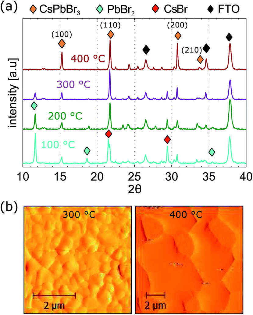 | ||
| Fig. 2 (a) XRD pattern of CsPbBr3 films post-annealed at 100, 200, 300 and 400 °C. The characteristic peaks of CsPbBr3 are marked with orange. Light blue and red markers indicate the presence of unconverted PbBr2 and CsBr precursor materials. FTO characteristic peaks are indicated by the black marker; (b) AFM amplitude images of CsPbBr3 films annealed at 300 and 400 °C respectively. | ||
X-Ray photoelectron spectroscopy (XPS) analysis was carried out to study any variations in the surface chemistry of CsPbBr3 films processed at different temperatures. Fig. 3(a) shows the XPS spectra of CsPbBr3 films processed at 100 and 400 °C. Raw data are fitted with Cs and Br doublets, the fitting spectra are shown in Fig. S3 in the ESI.† The intensity of the Cs(4d) doublet at 75.3 eV and Br(3d) doublet at 68 eV drop from 100 to 400 °C, indicating less unconverted CsBr and suggesting that high temperature annealing is necessary to obtain pure CsPbBr3. Notably, the peaks present after annealing at 400 °C are sharper than the ones measured for the film annealed at 100 °C. Sharp peaks indicate less complex chemistry, as the contribution from CsBr to the Br(3d) envelope drops. As XPS peaks are known to be sensitive to the local electronic environment, broad peaks can indicate disorder or subtle chemical shifts due to multiple similar bonding environments, hence the sharpening of peaks is consistent with the surface being predominantly one species (CsPbBr3) at 400 °C. The bottom graph in Fig. 3(b) shows the elemental ratios measured by XPS on different films. PbBr2 and CsBr ratios were measured directly from small amounts of powders of the precursor materials. The predicted Cs:Pb:Br ratio in the final perovskite films is the stoichiometric 1:1:3 ratio. The ratio Br:Pb at the surface exceeds 3:1 when the film is annealed at low temperatures, this is due to incomplete conversion of the precursors. Overall, an excess of CsBr was measured, especially when films were processed at 100 and 200 °C. When films were synthesised at 300 and 400 °C, the elemental ratio gets closer to the predicted stoichiometric perovskite ratio, suggesting that high temperature allows better conversion of precursors into CsPbBr3. The composition does not show a linear trend with temperature and a significant, non linear improvement in stoichiometry between 200 and 300 °C is observed. The top graph in Fig. 3(b) shows the amount of CsBr present on the top surface of the perovskite. The Cs content as CsBr on the surface decreases from about 30% to less than 10% with increasing annealing temperature. It is important to note that when the film is annealed at 400 °C a new compound develops. This compound is found as a Cs doublet at about 78 and 76 eV and it is present only in the film annealed at 400 °C (see Fig. S3 in the ESI†). The development of extra species is consistent with loss of electron density from the Cs atoms and hence possible oxidation of the material. It might be that 400 °C is a borderline temperature that pushes the CsPbBr3 perovskite very close to the edge of the process window.
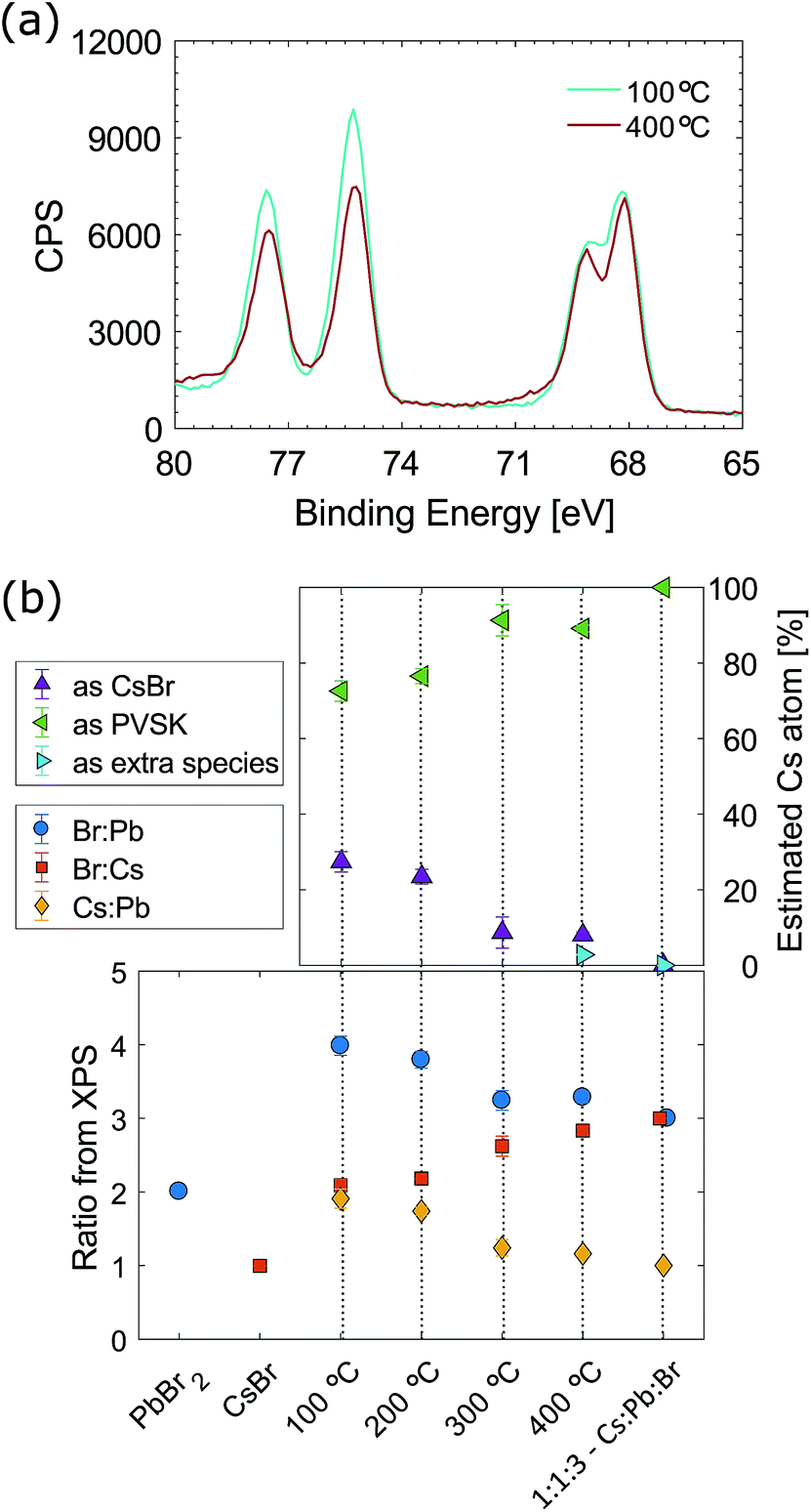 | ||
| Fig. 3 (a) Comparison of sets of doublets, Cs(4d) and Br(3d), measured by XPS on perovskite (PVSK) CsPbBr3 films processed at 100 and 400 °C; (b) variable surface chemistry of CsPbBr3 as films as a function of process temperature measured by XPS; all data are presented as ratios. Data are the average of three measurements, with error bars indicating the standard deviation. | ||
To evaluate device performance, solar cells were fabricated. Two different architectures based on carbon as hole transport layer were investigated. The first one is a multi-layer screen printed mesoporous stack with a carbon top electrode (mC-PSC). The mesoscopic layers involved are an n-type TiO2 layer, a ZrO2 layer acting as an insulating spacer and a mesoporous carbon top contact. CsPbBr3 is introduced by infiltration through the mesoporous stack. In this architecture, the crystal size of the CsPbBr3 should be determined by the pores of the mesoporous carbon structure, where the smallest were measured to be about 10 nm in width.24,48 The second architecture is a planar carbon solar cell, where the electron transport layer is TiO2 prepared by spray pyrolysis and the hole transport layer is carbon layer printed directly onto the CsPbBr3. In this architecture, the CsPbBr3 crystallite size is not limited by the carbon pore size.
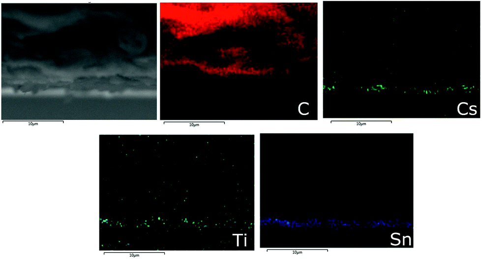
Fig. 4 shows cross section SEM/EDX images of a mC-PSC. EDX mapping allows a qualitative analysis of the elements present in the structure, providing details of the solution infiltration. In these devices, CsPbBr3 is homogeneously and uniformly infiltrated through the whole carbon layer. The three different mesoscopic layers are clearly defined and well separated from each other.
 | ||
| Fig. 4 Cross section SEM/EDX mapping of a mC-PSC device. The mesoscopic layers of TiO2, ZrO2 and C are indicated by light blue, purple and red colour respectively. Detection of CsPbBr3 is given by the green colour, which is assigned to Cs. The blue colour shows the presence of coated FTO on glass. | ||
J–V curves of four different mC-PSC annealed at 100, 200, 300 and 400 °C measured under reverse scan are shown in Fig. 5(a). The original J–V curves measured under forward and reverse scan are shown in Fig. S4 in the ESI.† The current density has been normalised to the Jsc to allow easier comparison of the curves. In all of the devices we observed very little change in the photocurrent density with post-annealing temperature. Indeed if the same cell was annealed and then re-measured at each of the four temperatures the short circuit current remained the same, but the fill factor was observed to drop due to repeated annealing of the same device (see Fig. S5 in the ESI†). The PV parameter that mainly changes with temperature is the open circuit voltage, as shown by the Voc trend with temperature in Fig. 5(b). The voltage improvement is non-linear as a function of processing temperature, showing a significant improvement between 200 and 300 °C. Interestingly, this trend corresponds well with the information on chemical composition obtained by XRD and XPS shown in Fig. 2 and 3. The composition may influence the recombination rate; unconverted CsPbBr3 species could limit the charge injection and transport, leading to accumulation of charges and higher interfacial recombination, which is reflected in a decreased Voc.2 Another factor influencing the voltage may be CsPbBr3 grain size. Fig. 2(b) showed that grains become larger when annealed at 400 °C. High temperature processing may push the infiltrated CsPbBr3 material to fully adhere with the carbon particles, improving the charge injection from the perovskite into the mesoporous carbon.
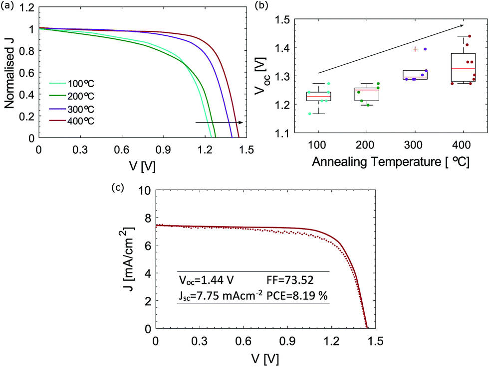 | ||
| Fig. 5 (a) J–V curves of a representative mC-PCS post annealed at different temperatures under reverse scan. The current density has been normalised to the Jsc. Original J–V curves can be found in Fig. S4 in the ESI; † (b) box-plots of Voc of mC-PSC annealed at different temperatures; (c) champion mC-PSC device post-annealed at 400 °C. | ||
Fig. 5(c) shows the champion mC-PSC device post-annealed at 400 °C, exhibiting Voc = 1.44 V, Jsc = 7.75 mA cm−2, FF = 73.52 and PCE = 8.19%. However, on some occasion loss in FF was observed for cells annealed at 400 °C (Fig. S5 and S8†). XPS analysis showed that when the film is processed at 400 °C, additional compounds develop on the surface, which might suggest oxidation and the edge of the process window. When processing CsPbBr3 films at 400 °C, oxidation of the material may be more or less pronounced due to small changes in the annealing temperature and heating and cooling time which may lead to more evident losses in the FF. Fig. S9(a)† shows the J–V curve of a mC-PSC post-annealed at 350 °C. No clear oxidation nor loss in FF are observed and high Voc of 1.35 V can be obtained. Stabilised power output measurements were also collected by monitoring the current when the cell was biased to the maximum power point voltage determined by the J–V sweep, showing a stable output over 60 s (Fig. S9(b) in the ESI†).
Recently, Liao et al. reported a CsPbBr3-based solar cell with quantum dots deposited at the ETM/CsPbBr3 and CsPbBr3/HTM interfaces respectively. They claim that the quantum dots create intermediate energy levels enhancing charge transfer and allowing a champion PCE of 8.2%.42 In this work we show that using a mesoporous architecture where CsPbBr3 is infiltrated through the mesoporous stack and post-annealed at 400 °C very high PCEs can be obtained without complex passivation of the interfaces.
Photovoltaic parameters shown as box plots for efficiency distributions of over 20 mC-PSC processed at 400 °C are presented in Fig. S10,† showing that very high voltages are consistently measured. Most notably, the average Voc is 1.27 V with the highest being 1.44 V. To our knowledge this is the highest voltage ever seen using the c-TiO2/m-TiO2/m-ZrO2/m-carbon structure-based cell, showing the potential of this architechture. Photocurrent densities for mC-PSC were found to change between 3.5 and 10 mA cm−2 over several batches (see Fig. S10†). We believe that the Jsc of mC-PSC mainly depends on how good the infiltration of CsPbBr3 into the mesoscopic porous carbon is. Similarly, Wagner et al., who studied the crystallisation of MAPI infiltrated in mesoporous carbon layers, noticed that the most significant increase in photocurrent was observed due to improved alignment of the perovskite surface to the porous carbon.48 The main parameters affecting the infiltration are believed to be the temperature of CsBr solution and the dipping time.40 The ramp rate to the high process temperature is another parameter that may play a significant role. Limited performance degradation was observed in mC-PSCs annealed at different temperatures. Fig. S12† shows the variation of the main PV parameters over time. During this time period, the cells were left in an ambient atmosphere without encapsulation, at open circuit (also known as shelf-stability).
Impedance measurements at open circuit were carried out to investigate recombination in mC-PSC when post-annealed at different temperatures. Fig. 6(a) illustrates the impedance response observed at open circuit for two different mC-PSC annealed at 100 and 400 °C. The Nyquist plots obtained for each device at all intensities are shown in Fig S13–S16 in the ESI.† At all intensities three semi-circles were seen in the Nyquist plots. The semicircles centred on 51.4 and 23.5 kHz are attributed to the geometric capacitance Cg and the recombination resistance Rrec. The variation of Rrec with open circuit voltage is shown in Fig. 6(b). Semilogaritmic plots for mC-PSC annealed at different temperatures have very similar slopes, therefore the cells have similar ideality factors ranging between 2.1 and 2.5.49 Interestingly, the cells fall into two groups: at the same voltage Rrec is lower in the cells annealed at 100 and 200 °C and higher in the cells annealed at 300 and 400 °C. The non-linear trend as a function of temperature corresponds well with the compositional improvement shown by XPS/XRD and the change in open circuit voltage shown in Fig. 3 and 5. These results highlight that the increased open circuit voltage measured for mC-PSC annealed at higher temperatures may be due to a decreased recombination rate.
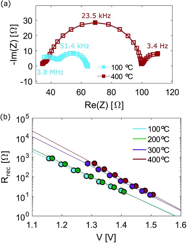 | ||
| Fig. 6 (a) Example of Nyquist plot of the mC-PSC annealed at 100 and 400 °C measured at 1.41 ± 0.01 V. The response of samples annealed at 100 °C was measured at the highest light intensity (λ = 465 nm, 1.47 × 1017 cm−2 s−1). While, the response of samples annealed at 400 °C was measured at a lower light intensity (λ = 465 nm, 1.47 × 1016 cm−2 s−1); (b) recombination resistance for the different type of mC-PSC at open circuit under different illumination intensities. Slopes of the lines shown are 148, 140, 132 and 124 mV per decade for samples annealed at 100, 200, 300 and 400 °C respectively. These values correspond to an ideality factor m of 2.5, 2.4, 2.2 and 2.1. | ||
The spectra were distorted at very high frequencies, with an additional semicircle appearing at the highest illumination intensities. This high frequency response did not change following annealing and we believe it is connected to the carbon contact. This would be expected as all the cells contain a carbon layer of similar thickness which was pre-annealed at 400 °C (Fig. S17 in the ESI† shows the dependence of the resistance extracted from the high frequency response on light intensity and annealing temperature). A third low-frequency (LF) semicircle was observed below 5 Hz, which became more defined for samples processed at higher temperatures. The low frequency response of perovskite solar cells is still hotly debated in the literature and is outside the scope of this paper. A similar low frequency response appeared in the impedance plots of standard planar MAPI cells and they were assigned to changes in the recombination resistance due to the motion of ionic vacancies.50
Fig. 7 shows the cross section SEM/EDX images of a C-PSC. In contrast to the mC-PSC, the carbon layer is screen printed on top of the CsPbBr3. Thin layers of c-TiO2 and CsPbBr3 are both below the thick porous carbon layer, which acts as hole transport material and top contact.
 | ||
| Fig. 7 Cross section SEM/EDX mapping of a C-PSC device. The thin layers of TiO2 and CsPbBr3 are indicated by light blue and green colour respectively. The thick carbon layer is mapped with the red colour. The blue colour shows the presence of coated FTO on glass. | ||
The effect of post-annealing on the planar C-PSC cells was also investigated and the results were compared to those for the mC-PSC. Annealing of C-PSC was carried out after the carbon layer was screen printed on top of the CsPbBr3 absorber layer in order to be consistent with the procedure used for the fabrication of mC-PSC and allow a proper comparison. Each device was systematically annealed at 100, 200, 300 and 400 °C and the same cell re-measured at each of the four temperatures. Fig. 8(a) shows the variation of the main photovoltaic parameters with annealing temperature. Post-annealing treatment at 400 °C is necessary to get high voltage and any performance. The conductivity of the carbon paste at different temperatures was measured using a 4-point probe system (Fig. S18†). The sheet resistance reaches a plateau at about 250 °C. However, the paste is already conducting at 100 °C. Previous TGA and XPS analysis of the sintered carbon paste showed that nitrocellulose binder is entirely eliminated after 400 °C.24 Baker et al. showed that residual non-conductive binder in the carbon layer introduces a band gap at the interface that affects the injection of charges, leading to poor performance.24 To verify the reproducibility of C-PSC, several batches were fabricated and measured on different days. All cells were made in air with relative humidity (RH) varying between 15 and 40%. The data obtained from 43 devices are shown as box plots in Fig. S19 in the ESI.† Mean and median of all PV parameters have very similar values, indicating that the distribution of data is symmetric. The average open circuit voltage is 1.33 V, with the maximum measured being 1.45 V. Liao et al. reported a CsPbBr3 carbon solar cell with a Voc of 1.47 V by depositing quantum dots layers at the ETM/CsPbBr3 and CsPbBr3/HTM interfaces to enhance the charge extraction. In cells with unmodified interfaces a Voc of 1.28 V was reported. In this work, we show that very high voltages can be obtained using CsPbBr3 as absorber material without interface modification.
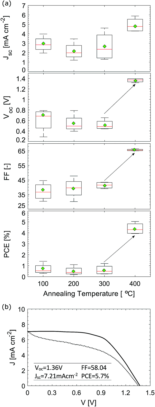 | ||
| Fig. 8 (a) Box plots of main PV parameters of several C-PSC processed at different temperatures; (b) J–V curves of the champion C-PSC annealed at 400 °C, achieving Voc = 1.36 V, Jsc = 7.21 mA cm−2, FF = 58.04 and PCE = 5.7%. | ||
Fig. 8(b) shows the J–V curve of the champion C-PSC, which exhibited Voc = 1.36 V, Jsc = 7.21 mA cm−2, FF = 58.04 and PCE = 5.7% in the reverse direction. The planar device exhibited hysteresis between the two scanning modes, revealing a PCE of 4.2% under forward scan (which leads to an average PCE of 4.95%). Hysteresis in perovskite solar cells is caused by ion migration and the severity of the effect is influenced by the nature of the contact layers.51,52 Careful selection of the electron transport material can reduce the phenomenon at room temperature. Thin layers of mesoporous TiO2 between the crystalline perovskite and c-TiO2 can result in solar cells with low hysteresis.52,53
Impedance measurements at open circuit were also carried out on C-PSCs post-annealed at 400 °C. Fig. 9(a) shows the Nyquist plots of a planar carbon cell post-annealed at 400 °C. As above, an additional semi-circle was observed at the highest frequencies which is likely caused by the carbon contact. The semi-circle centred on 2.5 kHz was attributed to Cg and the recombination resistance Rrec. The recombination resistance Rrec is shown in Fig. 9(b) as a function of Voc and compared to the Rrec calculated for a mC-PSC post-annealed at 400 °C. Planar cells show higher Rrec than mC-PSC, suggesting that on average planar devices should have lower recombination and higher Voc.
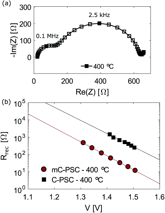 | ||
| Fig. 9 (a) Example of Nyquist plot of the C-PSC post-annealed at 400 °C measured at open circuit (1.47 V). The response was measured at a light intensity of λ = 465 nm, 1.47 × 1016 cm−2 s−1; (b) recombination resistance for the different type of CsPbBr3 carbon cells at open circuit under different illumination intensities. Slopes of the lines shown are 124 mV per decade for the mC-PSC and 131 mV per decade for the C-PSC, corresponding to ideality factors of 2.1 and 2.2, respectively. | ||
Fig. S21† shows the box plots of the main PV parameters of mC-PSC and C-PSC post-annealed at 400 °C, with the correspondent average values. Only mC-PSC processed at 400 °C were taken into account to allow a proper comparison between the mesoporous and the planar architecture. Overall, C-PSCs show higher open circuit voltage than mC-PSC devices, in agreement with the impedance measurements. On average, an increase of 0.5 V was measured. AFM images showed that CsPbBr3 grains enlarge considerably during the post-annealing treatment, especially at 400 °C. With increasing grain size, trap assisted recombination at the crystallite surface may be reduced and the open circuit voltage improved.54 In planar devices the growing CsPbBr3 crystallites are less constrained compared to mC-PSCs where the CsPbBr3 is infiltrated in the mesoscopic layers of ZrO2 and carbon and the matrix is likely to limit the crystallite size.
The average photocurrent is higher in mC-PSC. As reported in previous literature, the morphology of perovskite films strongly influence the performance of C-PSC.40 At 400 °C the grain size of CsPbBr3 increases and the surface becomes much more rough. High roughness might induce poor contact between the perovskite and the carbon HTM, resulting in a lower photocurrent. In contrast, in mC-PSC the contact between the CsPbBr3 and carbon is expected to be more efficient, as the perovskite material is in intimate contact with the mesoporous layer. However, the photocurrent of the mesoporous devices showed a much wider distribution. Similarly to observations on MAPI graphite-based PSC,48 the infiltration of CsPbBr3 and right alignment of the perovskite material within the carbon pores are crucial to achieve high photocurrents.
Conclusions
We have investigated planar and mesoporous solar cells using carbon as the hole extraction material and CsPbBr3 as absorber material. All-inorganic CsPbBr3 is much less volatile than the more commonly used organic methylammonium cation, therefore more thermally stable. The properties of CsPbBr3 films were investigated as a function of processing temperature, which was varied between 100 and 400 °C. High temperature annealing was found to be necessary to obtain pure phase materials and a post annealing temperature of 400 °C showed full conversion of the precursor materials PbBr2 and CsBr into CsPbBr3. After post-annealing at 400 °C in air, CsPbBr3 films with larger grains were achieved. XPS analysis suggested that the excess of CsBr decreases (non-linearly) with processing temperature, showing a clear shift to lower amounts of CsBr between 200 and 300 °C. Extra species were present only at 400 °C, suggesting oxidation of the surface and the edge of the process window.Two different architectures based on different electron transport materials and fabrication methods were compared. mC-PSC devices have a multi-layer screen printed mesoporous stack with CsPbBr3 introduced by infiltration. While in C-PSC a thin film of CsPbBr3 is sandwiched between a compact layer of TiO2 and a mesoporous thick layer of carbon. The photovoltage of mC-PSC measured from J–V curves and the recombination resistance extracted from impedance measurements showed a non-linear trend with processing temperature, with significant improvements between 200 and 300 °C, corresponding with the compositional improvements observed with XPS. The champion mC-PSC reached a PCE of 8.2% with a remarkable Voc of 1.44 V. C-PSC achieved good performance only when annealed at 400 °C. High temperature processing allows the complete release of non-conductive binder in the thick carbon electrode and higher voltages and FF. The champion C-PSC reached a PCE of 5.7%. Very high Voc were consistently measured on many devices (over 40 cells) fabricated in different batches, with an average of 1.33 V.
This is the first time such high photovoltages have been measured for c-TiO2/m-TiO2/m-ZrO2/m-carbon structure-based cell. Very promising results using CsPbBr3 for solar cell applications have been shown. The possibility of working with fully printable devices that tolerate high temperatures opens up new research to forward the commercialisation of perovskite solar cells.
Conflicts of interest
There are no conflicts to declare.Acknowledgements
We acknowledge the MAS staff at University of Bath for their assistance in SEM acquisition. I. P., S. E. and P. J. C. would like to thank the EPSRC Centre for Doctoral Training in Sustainable Chemical Technologies (EP/L016354/1). This project has received funding from the European Union's Horizon 2020 research and innovation programme H2020-MSCA-CO-FUND-2014 (# 665992, MSCA FIRE: Fellows with Industrial Research Enhancement). J. B., J. Mc, F. D. R and T. W. would like to thank the Self-Assembling Perovskite Absorbers – Cells Engineered into Modules (SPACE-Modules) (EP/M015254/2) and the SPECIFIC Innovation and Knowledge Centre (EP/N02083/1).References
- S. D. Stranks, P. K. Nayak, W. Zhang, T. Stergiopoulos and H. J. Snaith, Angew. Chem., Int. Ed., 2015, 54, 3240–3248 CrossRef PubMed.
- M. M. Lee, J. Teuscher, T. Miyasaka, T. N. Murakami and H. J. Snaith, Science, 2012, 338, 643–647 CrossRef PubMed.
- H.-S. Kim, C.-R. Lee, J.-H. Im, K.-B. Lee, T. Moehl, A. Marchioro, S.-J. Moon, R. Humphry-Baker, J.-H. Yum, J. E. Moser, M. Grätzel and N.-G. Park, Sci. Rep., 2012, 2, 591 CrossRef PubMed.
- W. S. Yang, B.-W. Park, E. H. Jung, N. J. Jeon, Y. C. Kim, D. U. Lee, S. S. Shin, J. Seo, E. K. Kim, J. H. Noh and S. I. Seok, Science, 2018, 356, 1376–1379 CrossRef PubMed.
- K. Domanski, J. P. Correa-Baena, N. Mine, M. K. Nazeeruddin, A. Abate, M. Saliba, W. Tress, A. Hagfeldt and M. Grätzel, ACS Nano, 2016, 10, 6306–6314 CrossRef PubMed.
- N. L. Chang, A. W. Yi Ho-Baillie, P. A. Basore, T. L. Young, R. Evans and R. J. Egan, Prog. Photovoltaics, 2017, 25, 390–405 Search PubMed.
- V. Mirruzzo and A. Di Carlo, Chem, 2017, 2, 612–613 Search PubMed.
- A. Abate, T. Leijtens, S. Pathak, J. Teuscher, R. Avolio, M. E. Errico, J. Kirkpatrik, J. M. Ball, P. Docampo, I. McPherson and H. J. Snaith, Phys. Chem. Chem. Phys., 2013, 15, 2572 RSC.
- I. Lee, J. H. Yun, H. J. Son and T.-S. Kim, ACS Appl. Mater. Interfaces, 2017, 9, 7029–7035 CrossRef PubMed.
- D. Bi, G. Boschloo and A. Hagfeldt, Nano, 2014, 09, 1440001 CrossRef.
- W. A. Laban and L. Etgar, Energy Environ. Sci., 2013, 6, 3249 RSC.
- S. D. Stranks, S. D. Stranks, G. E. Eperon, G. Grancini, C. Menelaou, M. J. P. Alcocer, T. Leijtens, L. M. Herz, A. Petrozza and H. J. Snaith, Science, 2014, 342, 341–344 CrossRef PubMed.
- Z. Ku, Y. Rong, M. Xu, T. Liu and H. Han, Sci. Rep., 2013, 3, 3132 CrossRef PubMed.
- A. Mei, X. Li, L. Liu, Z. Ku, T. Liu, Y. Rong, M. Xu, M. Hu, J. Chen, Y. Yang, M. Gratzel and H. Han, Science, 2014, 345, 295–297 CrossRef PubMed.
- L. Zhang, T. Liu, L. Liu, M. Hu, Y. Yang, A. Mei and H. Han, J. Mater. Chem. A, 2015, 3, 9165–9170 RSC.
- H. N. Chen, Z. H. Wei, H. X. He, X. L. Zheng, K. S. Wong and S. H. Yang, Adv. Energy Mater., 2016, 6, 1502087 CrossRef.
- H. Zhang, H. Wang, S. T. Williams, D. Xiong, W. Zhang, C. C. Chueh, W. Chen and A. K. Jen, Adv. Mater., 2017, 29, 1606608 CrossRef PubMed.
- H. Hu, B. Dong and W. Zhang, J. Mater. Chem. A, 2017, 5, 11436–11449 RSC.
- Y. Hu, Z. Zhang, A. Mei, Y. Jiang, X. Hou, Q. Wang and K. Du, Adv. Mater., 2018, 30, 1705786 CrossRef PubMed.
- Y. Rong, X. Hou, Y. Hu, A. Mei, L. Liu, P. Wang and H. Han, Nat. Commun., 2017, 33, 647–648 Search PubMed.
- G. Grancini, I. Zimmermann, E. Mosconi, D. Martineau and S. Narbey, Nat. Commun., 2017, 8, 1–8 CrossRef PubMed.
- S. Liu, W. Huang, P. Liao, N. Pootrakulchote, H. Li, J. Lu, J. Li, F. Huang, X. Shai, X. Zhao, Y. Shen, Y. B. Cheng and M. Wang, J. Mater. Chem. A, 2017, 5, 22952–22958 RSC.
- F. Matteocci, L. Cinà, E. Lamanna, S. Cacovich, G. Divitini, P. A. Midgley, C. Ducati and A. Di Carlo, Nano Energy, 2016, 30, 162–172 CrossRef.
- J. Baker, K. Hooper, S. Meroni, A. Pockett, J. McGettrick, Z. Wei, R. Escalante, G. Oskam, M. Carnie and T. Watson, J. Mater. Chem. A, 2017, 5, 18643–18650 RSC.
- S. M. Meroni, Y. Mouhamad, F. De Rossi, A. Pockett, J. Baker, R. Escalante, J. Searle, M. J. Carnie, E. Jewell, G. Oskam and T. M. Watson, Sci. Technol. Adv. Mater., 2018, 19, 1–9 CrossRef.
- F. De Rossi, J. Baker, D. Beyon, K. Hooper, S. Meroni, D. Williams, Z. Wei, A. Yasin, C. Charbonneau, E. Jewell and T. M. Watson, Adv. Mater. Technol., 2018, 1800156 CrossRef.
- S. Ryu, J. H. Noh, N. J. Jeon, Y. Chan Kim, W. S. Yang, J. Seo and S. I. Seok, Energy Environ. Sci., 2014, 7, 2614–2618 RSC.
- P. Sullivan, S. Schumann, R. Da Campo, T. Howells, A. Duraud, M. Shipman, R. A. Hatton and T. S. Jones, Adv. Energy Mater., 2013, 3, 239–244 CrossRef.
- W. S. dos Santos, M. Rodriguez, J. M. Khoury, L. A. Nascimento, R. J. Ribeiro, J. P. Mesquita, A. C. Silva, F. G. Nogueira and M. C. Pereira, ChemSusChem, 2018, 11, 589–597 CrossRef PubMed.
- M. Saliba, T. Matsui, J.-Y. Seo, K. Domanski, J.-P. Correa-Baena, M. K. Nazeeruddin, S. M. Zakeeruddin, W. Tress, A. Abate, A. Hagfeldt and M. Grätzel, Energy Environ. Sci., 2016, 9, 1989–1997 RSC.
- B. Li, Y. Zhang, L. Fu, T. Yu, S. Zhou, L. Zhang and L. Yin, Nat. Commun., 2018, 9, 1–8 CrossRef PubMed.
- B. Jeong, H. Han, Y. J. Choi, S. H. Cho, E. H. Kim, S. W. Lee, J. S. Kim, C. Park, D. Kim and C. Park, Adv. Funct. Mater., 2018, 28, 1–8 Search PubMed.
- L. Yan, Q. Xue, M. Liu, Z. Zhu, J. Tian, Z. Li, Z. Chen, Z. Chen, H. Yan, H.-L. Yip and Y. Cao, Adv. Mater., 2018, 1802509 CrossRef PubMed.
- R. E. Beal, D. J. Slotcavage, T. Leijtens, A. R. Bowring, R. A. Belisle, W. H. Nguyen, G. F. Burkhard, E. T. Hoke and M. D. McGehee, J. Phys. Chem. Lett., 2016, 7, 746–751 CrossRef PubMed.
- M. Kulbak, D. Cahen and G. Hodes, J. Phys. Chem. Lett., 2015, 6, 2452–2456 CrossRef PubMed.
- M. Kulbak, S. Gupta, N. Kedem, I. Levine, T. Bendikov, G. Hodes and D. Cahen, J. Phys. Chem. Lett., 2016, 7, 167–172 CrossRef PubMed.
- J. Lei, F. Gao, H. Wang, J. Li, J. Jiang, X. Wu, R. Gao, Z. Yang and S. Liu, Sol. Energy Mater. Sol. Cells, 2018, 187, 1–8 CrossRef.
- C. C. Stoumpos, C. D. Malliakas, J. A. Peters, Z. Liu, M. Sebastian, J. Im, T. C. Chasapis, A. C. Wibowo, D. Y. Chung, A. J. Freeman, B. W. Wessels and M. G. Kanatzidis, Cryst. Growth Des., 2013, 13, 2722–2727 CrossRef.
- J. Liang, C. Wang, Y. Wang, Z. Xu, Z. Lu, Y. Ma, H. Zhu, Y. Hu, C. Xiao, X. Yi, G. Zhu, H. Lv, L. Ma, T. Chen, Z. Tie, Z. Jin and J. Liu, J. Am. Chem. Soc., 2016, 138, 15829–15832 CrossRef PubMed.
- X. Chang, W. Li, L. Zhu, H. Liu, H. Geng, S. Xiang, J. Liu and H. Chen, ACS Appl. Mater. Interfaces, 2016, 8, 33649–33655 CrossRef PubMed.
- Z. Liu, B. Sun, X. Liu, J. Han, H. Ye, T. Shi, Z. Tang and G. Liao, Nano-Micro Lett., 2018, 10, 34 CrossRef.
- G. Liao, J. Duan, Y. Zhao and Q. Tang, Sol. Energy, 2018, 171, 279–285 CrossRef.
- H. Yuan, Y. Zhao, J. Duan, B. He, Z. Jiao and Q. Tang, Electrochim. Acta, 2018, 279, 84–90 CrossRef.
- Q. A. Akkerman, M. Gandini, F. Di Stasio, P. Rastogi, F. Palazon, G. Bertoni, J. M. Ball, M. Prato, A. Petrozza and L. Manna, Nat. Energy, 2017, 2, 1–7 Search PubMed.
- N. K. Kumawat, N. Jain, A. Dey, K. L. Narasimhan and D. Kabra, Adv. Funct. Mater., 2017, 27, 1603219 CrossRef.
- S. Ahmad and G. V. Prakash, Opt. Mater. Express, 2014, 4, 101 CrossRef.
- Lovkush, C. Ravikant, P. Arun and K. Kumar, Mater. Res. Express, 2016, 3, 076403 CrossRef.
- L. Wagner, L. E. Mundt, G. Mathiazhagan, M. Mundus, M. C. Schubert, S. Mastroianni, U. Würfel, A. Hinsch and S. W. Glunz, Sci. Rep., 2017, 7, 1–6 CrossRef PubMed.
- A. Pockett, G. E. Eperon, T. Peltola, H. J. Snaith, A. B. Walker, L. M. Peter and P. J. Cameron, J. Phys. Chem. C, 2015, 119, 3456–3465 CrossRef.
- A. Pockett, G. E. Eperon, N. Sakai, H. J. Snaith, L. M. Peter and P. J. Cameron, Phys. Chem. Chem. Phys., 2017, 19, 5959–5970 RSC.
- H. J. Snaith, A. Abate, J. M. Ball, G. E. Eperon, T. Leijtens, N. K. Noel, S. D. Stranks, J. T. W. Wang, K. Wojciechowski and W. Zhang, J. Phys. Chem. Lett., 2014, 5, 1511–1515 CrossRef PubMed.
- S. V. Reenen, M. Kemerink and H. J. Snaith, J. Phys. Chem. Lett., 2015, 6, 3808–3814 CrossRef PubMed.
- W. S. Yang, J. H. Noh, N. J. Jeon, Y. C. Kim, S. Ryu, J. Seo and S. I. Seok, Science, 2015, 348, 1234–1237 CrossRef PubMed.
- H. D. Kim, H. Ohkita, H. Benten and S. Ito, Adv. Mater., 2016, 28, 917–922 CrossRef PubMed.
Footnote |
| † Electronic supplementary information (ESI) available. See DOI: 10.1039/c8ta07694d |
| This journal is © The Royal Society of Chemistry 2018 |