
 Open Access Article
 This Open Access Article is licensed under a
 Creative Commons Attribution 3.0 Unported Licence
Formation and suppression of defects during heat treatment of BiVO4 photoanodes for solar water splitting†
Marlene
Lamers
,
Sebastian
Fiechter
,
Dennis
Friedrich
 ,
Fatwa F.
Abdi
* and
Roel
van de Krol
*
,
Fatwa F.
Abdi
* and
Roel
van de Krol
*
Institute for Solar Fuels, Helmholtz-Zentrum Berlin für Materialien und Energie GmbH, Hahn-Meitner-Platz 1, Berlin 14109, Germany. E-mail: fatwa.abdi@helmholtz-berlin.de; roel.vandekrol@helmholtz-berlin.de
First published on 17th September 2018
Abstract
Metal oxide photoelectrodes typically suffer from poor carrier transport properties and extensive carrier recombination, which is caused by the presence of intrinsic or extrinsic defects in the material. Here, the influence of annealing temperature and atmosphere on the formation and suppression of defects in BiVO4—one of the best performing metal oxide photoanodes—is elucidated. Annealing in argon has little or no effect on the photoelectrochemical performance due to the competing effects of an increase in grain size (i.e., reduction of grain boundaries) and the unfavorable formation of oxygen vacancies. When annealing in air, the formation of oxygen vacancies is suppressed, resulting in up to ∼1.5-fold enhancement of the photocurrent and an order of magnitude increase of the charge carrier mobility. However, vanadium leaves the BiVO4 lattice above 500 °C, which leads to a decrease in carrier lifetime and photocurrent. This vanadium loss can be avoided by supplying excess vanadium in the gas phase during annealing. This leads to enhanced charge carrier mobility and lifetime, resulting in improved photocurrents. Overall, this strategy offers a general approach to prevent unfavorable changes of cation stoichiometry during high-temperature treatment of complex metal oxide photoelectrodes.
Introduction
Photoelectrochemical (PEC) water splitting is a promising pathway for renewable energy production. Using a semiconductor immersed in an aqueous electrolyte, water is converted into hydrogen and oxygen by solar irradiation. Typically, this process can be divided into (i) light absorption in the semiconducting photoelectrode to generate charge carriers (electrons and holes), (ii) separation of the charge carriers, and (iii) water oxidation and/or reduction at the surface of the electrodes.1 Metal oxides are particularly attractive as photoelectrode materials, mainly due to their generally good aqueous stability, non-toxicity, and low cost.2–4 However, their PEC activities are typically limited by bulk recombination, which is partly due to the presence of defects. Metal oxide photoelectrodes are often synthesized with low- or moderate-temperature processes, such as drop casting, spray pyrolysis, or electrodeposition. Although the simplicity of such processes offers important advantages, it tends to create relatively high defect densities (>1018 cm−3) in the form of intrinsic point defects (e.g., cation and oxygen vacancies) as well as non-crystalline phases.5 While some of these defects can promote the conductivity and therefore improve the PEC performance of the photoelectrode material,6–9 many of these defects form electronic states deep in the bandgap of the oxide. Such states act as efficient charge carrier trapping or recombination centers, resulting in short carrier lifetimes. In addition, the electronic structure of many metal oxides results in large effective masses for the electrons and holes. In combination with the typical polaronic nature of electronic charge transport, this results in poor charge carrier mobilities.10,11 It is the combination of short lifetimes and poor carrier mobilities that causes short carrier diffusion lengths and, therefore, recombination of the carriers before they are able to reach the interface.The above-mentioned limitations also apply to bismuth vanadate (BiVO4), which is one of the best performing metal oxide photoanodes for solar water splitting. The monoclinic scheelite phase, which is the most photoactive one, has a bandgap of 2.4–2.5 eV.12 Carrier transport in the material is slow, with reported carrier mobilities in the range of 10−2–10−1 cm2 V−1 s−1.10,13,14 In addition to having a small polaron conduction mechanism,10,11,15–17 the presence of defects in BiVO4 may lead to trap-mediated transport and/or bound polarons that reduce the mobility even further.13,14,18 Nevertheless, through various developments in the last 5–10 years, ∼90% of the theoretical maximum photocurrent of BiVO4 (7.5 mA cm−2, assuming all AM1.5 photons with energy higher than the 2.4 eV bandgap contribute to the photocurrent) has already been achieved.19 Pihosh et al. realized this record photocurrent by depositing a thin layer of BiVO4 onto WO3 nanorods to form a guest–host nanostructured photoelectrode. This orthogonalizes the direction of optical absorption and charge transport,20,21 which ensures that enough photons can be absorbed while the photogenerated carriers only need to travel short distances.
Despite these encouraging results, the fabrication of a complete solar water splitting device with a nanostructured BiVO4 photoanode is not straightforward. To generate the ∼1.5 V needed for water splitting, the BiVO4 is usually placed in front of one or two smaller-bandgap semiconductors to form a tandem device.22,23 Unfortunately, extensive optical scattering from nanostructured BiVO4 photoelectrodes prevents the low energy photons from reaching the bottom absorber. To circumvent this, Pihosh et al. used Pt as a reflective substrate and placed a double-junction GaAs/InGaAsP tandem solar cell in front of their BiVO4 at a 45° angle. The highly efficient III–V tandem cell absorbed enough of the diffusely back-reflected photons from the WO3/BiVO4 nanowires to reach an impressive 8.2% solar-to-hydrogen efficiency.19 In another report a beam splitter was used to direct the short wavelength part of the solar spectrum to the WO3/BiVO4 electrode and the long wavelength part to a perovskite solar cell, resulting in a device with a 7.7% solar-to-hydrogen efficiency.24 For practical applications, however, a simple stacked tandem configuration with a non-scattering top absorber (and without expensive III–V semiconductors) is preferred.25 To reduce the scattering of the WO3/BiVO4 nanowires one could revert to photolithographic techniques to create highly regular WO3 nanopillars followed by atomic layer deposition to deposit a BiVO4 top layer with a homogeneous thickness. In this paper, we aim for a potentially easier approach, which is to improve the carrier transport properties of the BiVO4. If successful, this would avoid the need for nanostructuring altogether.
One possible way to alleviate carrier transport limitations is to apply a high temperature treatment that may reduce the concentration of point defects and improve the crystallinity.26,27 While changes in the crystallinity can be readily observed by X-ray diffraction, changes in the nature and concentration of point defects are more difficult to track. To the best of our knowledge, no systematic studies have yet been carried out that correlate the influence of such heat treatments on the defect properties and the resulting PEC performance. In this paper, we systematically elucidate for the first time the formation of defects in BiVO4 thin films at high temperature in both oxidizing and reducing environments. We find that high temperature treatments of BiVO4 in air lead to an increase in grain size and improved carrier dynamics. At temperatures above 500 °C, however, vanadium is lost from the lattice. The concomitant decrease in photocurrent is presumably caused by the formation of vanadium vacancies. By introducing excess vanadium (V) in the gas phase during the heat treatment the formation of these vacancies can be avoided, leading to improved photocurrents.
Results and discussion
We first investigated the formation of defects in BiVO4 at high temperature. Mass spectroscopy (MS) was performed on BiVO4 powders to analyze possible losses of chemical species during heat treatment. BiVO4 powders were heated to 700 °C in air at a ramp rate of 7 °C min−1 and then kept at this temperature. The MS signals represented as ion currents are shown in Fig. 1 as a function of time and temperature. Signals of V+ (mass/charge ratio, m/q, of 51, green curve), VO+ (m/q = 67, blue curve) and VO2+ (m/q = 83, purple curve) are clearly detected, indicating vanadium loss from the BiVO4 powders at temperatures above 450 ± 20 °C. At the same time, no Bi+ (m/q = 209, red curve) or BiO− (−m/q = 225, orange curve) signals are detected. The vanadium loss also occurs in thin films of BiVO4; XPS measurements reveal that the V![[thin space (1/6-em)]](https://www.rsc.org/images/entities/char_2009.gif) :Bi ratio decreases from 0.76 for the film heated at 450 °C to 0.69 for the one heated at 700 °C (Fig. S1†). This is in agreement with a report by Wang et al.,28 in which BiVO4 films heated at temperatures higher than 500 °C showed a decrease in the V:Bi ratio. Longer measurements of up to 8 hours show negligible change in the rate of vanadium loss (Fig. S2†), and the rate follows the applied temperature. To further confirm the temperature at which the properties of BiVO4 thin films start to change, we performed an in situ UV-Vis measurement of a BiVO4 film heated in air. An increase of the absorption at around 500 nm (i.e., a darkening of the film) was observed at temperatures above ∼470 °C (Fig. S3†), which is in good agreement with the onset of vanadium loss found from the MS measurements.
:Bi ratio decreases from 0.76 for the film heated at 450 °C to 0.69 for the one heated at 700 °C (Fig. S1†). This is in agreement with a report by Wang et al.,28 in which BiVO4 films heated at temperatures higher than 500 °C showed a decrease in the V:Bi ratio. Longer measurements of up to 8 hours show negligible change in the rate of vanadium loss (Fig. S2†), and the rate follows the applied temperature. To further confirm the temperature at which the properties of BiVO4 thin films start to change, we performed an in situ UV-Vis measurement of a BiVO4 film heated in air. An increase of the absorption at around 500 nm (i.e., a darkening of the film) was observed at temperatures above ∼470 °C (Fig. S3†), which is in good agreement with the onset of vanadium loss found from the MS measurements.
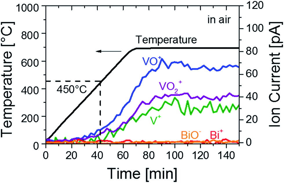 | ||
| Fig. 1 Mass spectroscopy (MS) analysis of BiVO4 powders in air. Temperature–time curve during the MS analysis (black) and ion currents for mass-to-charge ratios (m/q) of 51, 67, 83, 209, and 225, which correspond to V+ (green), VO+ (blue), VO2+ (purple), Bi+ (red) and BiO− (orange), respectively. | ||
The influence of vanadium loss on the crystal structure of BiVO4 thin films was studied by X-ray diffraction. Fig. 2 shows the grazing incidence X-ray diffractograms of as-prepared and annealed BiVO4 films deposited on fused silica (‘quartz’) substrates. All films show a pure monoclinic (scheelite-type) BiVO4 phase (clinobisvanite; space group: I2/b JCPDS card No. 14-0688) without any phase segregation. However, at temperatures of 600 °C and above, a re-orientation of the crystal lattice starts to occur and a strong preference for the (010) orientation is observed after annealing at 700 °C. This orientation is known to result in an enhanced photoelectrochemical performance.29,30 We attribute this re-orientation to changes in the amount of strain in the film, as caused by the vanadium loss and/or possible change in particle size.31 This is supported by the increased preference for the (010) orientation when uniaxially pressing BiVO4 powder into a pellet (Fig. S4†). The re-orientation of the crystal structure is also accompanied by a shift of the symmetric V–O stretching mode peak (∼826 cm−1) to a higher wavenumber, as shown in the Raman spectra (Fig. S5†). Since the wavenumber is inversely correlated with the interatomic distance,32 the observed shift can be attributed to a decrease in V–O bond length, which is consistent with the loss of vanadium that occurs under these conditions (Fig. 1).
 | ||
| Fig. 2 Grazing incidence X-ray diffraction patterns of BiVO4 films on quartz annealed in air at temperatures between 450 °C (black) and 700 °C (red). The labels indicate the diffraction peaks of the monoclinic scheelite crystal structure of BiVO4. | ||
To understand the influence of the annealing atmosphere, we performed the same high temperature MS measurement under argon flow. In contrast to the measurement in air (Fig. 1), neither V nor Bi loss was detected (Fig. S6†). Based on this, we conclude that the observed VO and VO2 species in the air-annealing experiment were formed by reaction of vanadium with oxygen from the environment and not oxygen from the lattice of BiVO4. The following defect-chemical reactions (in Kröger–Vink notation33) are proposed to describe the loss of vanadium:
 | (1) |
 | (2) |
It should be noted that a formal oxidation state of −5 for the vanadium vacancy  is energetically highly unfavorable so that it is likely to spontaneously ionize to the −4 or −3 state:
 | (3) |
Since no elemental V loss was observed in the Ar-annealing experiment, the presence of V (g) when annealing in air is believed to be the product of the following disproportionation reaction:
| 2VO (g) ⇌ VO2 (g) + V (g) | (4) |
Indeed, the change of Gibbs free energy, ΔG, for reaction (4) is negative (−61.6 kJ mol−1 at 500 °C), suggesting that the reaction is spontaneous. The activation energy for the formation of  in BiVO4 can be determined from an Arrhenius plot of the log of the ion current vs. the reciprocal temperature (Fig. S7†). The activation energies for reactions (2) and (3) are found to be 0.18 ± 0.02 eV and 0.23 ± 0.01 eV, respectively.
To investigate the influence of vanadium vacancies on the photoelectrochemical (PEC) performance, we fabricated thin film BiVO4 samples on FTO-coated glass substrates annealed under different temperatures and atmospheres as described in the Experimental section. The temperatures were limited between 450 and 550 °C, since scanning electron micrographs showed that agglomeration of the films starts to occur at temperatures above 550 °C (Fig. S8†). Within this temperature range, the crystal structure and orientation of the films do not change significantly (see Fig. 2). Since we are interested in the bulk charge separation properties of the films, the PEC measurements were performed in a 0.1 M phosphate buffer electrolyte (pH ∼ 7) with Na2SO3 added as a hole scavenger to remove any surface catalytic limitations. Fig. 3 shows the AM1.5 photocurrents at 1.2 V vs. RHE for BiVO4 films annealed at different temperatures up to 550 °C in air (black) and argon (purple) atmospheres. The heating atmosphere is found to have a profound influence on the resulting PEC performance. Annealing in Ar does not result in any change in the photocurrent of BiVO4. In contrast, the photocurrent is strongly affected by heat treatment in air. The photocurrent increases with increasing temperature until it reaches a maximum (∼1.5 fold increase) at about 500 °C. Above this temperature, the photocurrent decreases with increasing temperature.
 | ||
| Fig. 3 AM1.5 photocurrent of BiVO4 films annealed in different atmospheres (air and argon) at different temperatures. The photocurrents were measured under back-side illumination at 1.2 V vs. RHE, the electrolyte is 0.1 M potassium phosphate buffer (pH ∼ 7) with 0.5 M Na2SO3 as a hole scavenger. | ||
Since the PEC measurements were performed with Na2SO3 as a hole scavenger, charge transfer limitations at the BiVO4/electrolyte interface do not play a role. Thus, the observed temperature dependence is unlikely to be caused by any changes in the surface chemistry. We further rule out this possibility by comparing the oxidation states of Bi and V in BiVO4 films annealed at 450 °C and 500 °C in air and Ar with XPS (Fig. S9†). The peak positions of all core levels remain the same, indicating no changes in the oxidation states of Bi and V despite the significant differences in the PEC performance. The lack of a peak shift is not surprising, considering that even a large amount of vanadium vacancies (1018–1019 cm−3) would still be much lower than the ∼1 at% detection limit of XPS. Furthermore, the photocurrent onset potential shows negligible variation with annealing temperature and atmosphere (see Fig. S10†), which further confirms that the heat treatments do not significantly affect the surface chemistry of the material.
Morphological changes with increasing temperature may also be the reason behind the observed PEC behavior. As shown in Fig. S8,† the grain size indeed increases with increasing annealing temperature. However, this is true for BiVO4 films annealed in air as well as those annealed in argon; thus, changes in morphology cannot explain the differences in photocurrent. Cross-section SEM images of the films show that the thickness of the films shows little change (Fig. S11†), and AFM measurements (Table S1†) reveal that the specific surface area of the films is also not significantly affected by the heat treatment.
We also rule out changes in optical absorption as a possible cause, since the monotonic increase of the long wavelength absorption with temperature (see Fig. S12†) is inconsistent with the observed photocurrent maximum at 500 °C in Fig. 3.
With changes in surface chemistry and film morphology being ruled out, we attribute the observed differences in PEC performance to the formation and reduction of defects in BiVO4. For samples annealed in air, the increase in grain size reduces the amount of grain boundary scattering, leading to an increase in photocurrent with temperature up to 500 °C (Fig. 3). Annealing in argon also results in larger grains, but, in contrast to air annealing, also leads to the formation of oxygen vacancies,  . The formation of oxygen vacancies is evidenced by the loss of O2 without the accompanying loss of Bi or V, as shown in Fig. S6.† While the presence of
  can improve the conductivity, too many oxygen vacancies may reduce the space charge width and adversely affect charge separation. Moreover, it has been reported that
  can form deep trap states and act as recombination centers.34 This would cancel out the positive effect of the larger grain size and would explain the slight decrease in photocurrent for samples annealed in argon (Fig. 3). Anodic electrochemical treatment (i.e., applying positive bias) does not positively affect the photocurrent (Fig. S13†); thus, it seems not possible to re-fill the oxygen vacancies in our Ar-annealed BiVO4. At temperatures above 500° the photocurrent for samples annealed in air rapidly decreases (Fig. 3, black curve). Under these conditions the MS experiments showed a rapid loss of vanadium in the form of VO+, VO2+, and V+ (Fig. 1). This results in the formation of vanadium vacancies according to reactions (1) and (2). These have been reported to lie ∼0.3 eV above the valence band edge,35 which would be deep enough in the bandgap to form trap states and act as recombination centers. In contrast, no vanadium loss is observed when annealing in argon (Fig. S6†), nor does the photocurrent show any decrease under these conditions (Fig. 3, blue curve). Based on these observations, we conclude that the decrease in photocurrent for BiVO4 films annealed in air above 500 °C is due to the formation of vanadium vacancies.
We note that extending the annealing time of the BiVO4 films from 2 to 8 h at 500 °C in air also results in a lower PEC performance (Fig. S14†). We attribute this to the same V loss that causes the formation of V vacancies, which already starts at ∼450 °C (see Fig. 1).
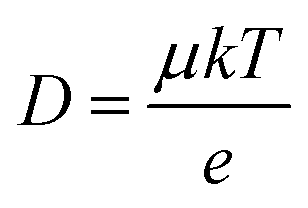
The carrier transport properties of the air-annealed BiVO4 films are investigated using time-resolved microwave conductivity (TRMC). Typical TRMC curves (ϕΣμ vs. time) are shown in Fig. S15;† the carrier mobility can be obtained from the peak amplitude, and the carrier lifetime can be obtained from the decay of the transient curve.36Table 1 summarizes the TRMC results obtained at a laser pulse intensity of 3.5 × 10¹³ photons per pulse per cm2. Consistent with our previous report,13 the carrier mobility (μ) of BiVO4 annealed in air at 450 °C is rather low at ∼0.02 cm2 V−1 s−1, while its carrier lifetime (τ) of ∼70 ns is relatively long. The carrier diffusion length (LD) can be calculated using the following equation:
 | (5) |
 | (6) |
 . Although not yet dominating at this temperature, vanadium vacancies are likely to be formed as a result of the vanadium loss at temperatures above ∼450 °C (see Fig. 1). As discussed above, these vacancies may act as deep defect states that cause recombination and therefore decrease the carrier lifetime. The net effect of the ∼10× increase in mobility and the ∼3× decrease in lifetime is an increase of the carrier diffusion length to ∼105 nm, which explains the observed increase of photocurrent when BiVO4 is annealed in air up to 500 °C (Fig. 3). Above 500 °C, the formation of
  dominates, which leads to increased recombination. Table 1 indeed shows decreased carrier mobility and lifetime of the BiVO4 film annealed in air at 550 °C. The diffusion length decreases to ∼32 nm, consistent with the decrease in photocurrent observed in Fig. 3.
| Temperature | Carrier mobility μ (10−2 cm2 V−1 s−1) | Carrier lifetime τ (ns) | Diffusion length LD (nm) |
|---|---|---|---|
| 450 °C in air | 2 ± 0.4 | 68.8 ± 2.6 | 59.7 ± 0.3 |
| 500 °C in air | 21 ± 0.8 | 20.5 ± 1.4 | 105.5 ± 1.6 |
| 550 °C in air | 2 ± 0.1 | 19.7 ± 2.3 | 31.9 ± 0.1 |
| 550 °C in air + BiVO4 powder | 13.5 ± 2.5 | 34.7 ± 0.8 | 110.1 ± 0.9 |
It should be noted that diffusion of impurities from the FTO substrate (e.g. Sn from the F:SnO2 or Na from the glass) during high-temperature treatments may also affect the properties of the BiVO4. However, the transport properties measured by TRMC, which were obtained using Na- and Sn-free quartz substrates, show the same trends as the photocurrents that were measured using FTO substrates. Moreover, impurity diffusion cannot explain the pronounced influence of the annealing atmosphere that is observed in Fig. 3 and 4. Therefore, impurity diffusion is unlikely to play an important role in our experiments.
 | ||
| Fig. 4 AM1.5 photocurrent–voltage curve of BiVO4 films annealed in air and BiVO4 atmosphere at 450 and 550 °C. The photocurrents were measured under back-side illumination in 0.1 M potassium phosphate buffer (pH ∼ 7) with 0.5 M Na2SO3 as a hole scavenger. The dark current is shown in gray. | ||
Our findings show that when BiVO4 is annealed at high temperature in air, the resulting loss of vanadium is detrimental to the PEC performance. As a strategy to overcome the vanadium loss, we annealed our BiVO4 film in the presence of BiVO4 powder (see Experimental section). By ensuring that the amount of BiVO4 powder exceeds the amount of BiVO4 in the film by several orders of magnitude, we create a VOx-rich atmosphere during the annealing. The high concentration of VOx species is then expected to shift the defect equilibrium of reactions (1) and (2) to the left and thus suppress the vanadium loss from the BiVO4 film. Under these conditions, no re-orientation of the crystal lattice is observed, even after annealing at temperatures as high as 700 °C (Fig. S16†). This suggests that the re-orientation of crystallites in the films is indeed induced by the loss of vanadium from the films. The exact mechanism of this re-orientation is still unclear and beyond the scope of the current study.
Fig. 4 shows that annealing in a VOx-rich atmosphere can partially compensate the loss of photocurrent observed in Fig. 3 when heating the films at 550 °C in air. This partial recovery is consistent with the improved carrier transport properties as measured by TRMC; annealing in VOx-rich atmosphere results in a 3.4-fold increase in the carrier diffusion length (Table 1).
Fig. 5 summarizes our findings on the influence of different annealing atmospheres on the properties of BiVO4 thin films. In all cases, the grain size of BiVO4 increases with increasing temperature, which results in a reduced number of grain boundaries and higher carrier mobilities. However, annealing in Ar introduces oxygen vacancies, which act as trap states in the film. This reduces the carrier lifetime and therefore nullifies the positive effect of larger grain sizes. The formation of oxygen vacancies can be prevented by annealing the samples in air. Unfortunately, the presence of air results in the loss of vanadium via volatile VOx species, especially above 500 °C. This is accompanied by a decrease in the photocurrent, which is presumably caused by the formation of vanadium vacancies that act as recombination centers. This can be avoided by annealing in the presence of BiVO4 powder in order to create a VOx-rich atmosphere. This prevents the formation of both oxygen vacancies and vanadium vacancies, and results in a BiVO4 film with higher carrier mobility and lifetime. This increases the carrier diffusion length and, therefore, the photocurrent of the films.
 | ||
| Fig. 5 Schematic illustration of the influence of annealing atmosphere on the morphology, defect formation, and carrier transport properties in BiVO4. | ||
Experimental section
Synthesis
100 nm-thick BiVO4 films were prepared by spray pyrolysis following a previously reported method.14,38–40 Briefly, a fluorine-doped tin oxide (FTO) coated glass substrate (TEC7, Pilkington) or quartz substrate (polished, Spectrosil 2000, Heraeus) was kept at 450 °C on a hot plate during the spray pyrolysis. The precursor solution was prepared by dissolving 0.4 mmol VO(C2H7O2)2 (99%, Alfa Aesar) and 0.4 mmol Bi(NO3)3·5H2O (98%, Alfa Aesar) in 100 mL solvent consisting of acetic acid (98%, Sigma Aldrich) and ethanol (Sigma Aldrich) in a 1:9 ratio. The solution was sprayed on the heated substrate in 100 cycles with a spray rate of ∼1 nm per cycle. The as-deposited films were then post-annealed in air at 450 °C for 2 h. Further heat treatments of the films are described in the Results and discussion section. In order to create a BiVO4-rich atmosphere, 0.6 g of BiVO4 powder (pure DCCM-137, Dominion Colour Corporation) was placed in the oven during the high temperature treatment of the BiVO4 films. This amount was calculated to be ∼4 orders of magnitude higher than the amount of BiVO4 in the 100 nm-thick film.
Materials characterization
Mass spectrometry analysis was performed using a Netzsch thermobalance STA409C coupled with a mass spectrometer, which was operated under a continuous flow of Ar or synthetic air (80 mL min−1). The commercially-obtained BiVO4 powder (see Synthesis section) was placed in an Al2O3 crucible and fixed to the sample holder of the thermobalance. X-ray diffraction (XRD) was conducted with a Bruker D8 diffractometer using a Cu Kα radiation (λ = 1.54184 Å) at 40 kV and 40 mA. This measurement was done in a grazing incidence configuration with a 0.5° incident angle. A Horiba HR800 spectrometer with a HeNe laser was used for Raman spectroscopy. The HeNe laser is a 500:1 polarized 20 mW laser with a wavelength of 632.8 nm. Scanning electron microscopy (SEM) images were taken using a LEO GEMINI 1530 with an acceleration voltage of 3 kV. The BiVO4 films were coated with a thin carbon layer to prevent charging during the SEM measurements. UV-Vis spectroscopy was performed in an integrating sphere using a Lambda 950 spectrophotometer (Perkin Elmer) in a wavelength range from 320 to 800 nm. High temperature in situ UV-Vis spectroscopy measurements were performed by placing the BiVO4 films on a sample holder in a custom quartz tube equipped with a flat quartz window, as described previously.41,42 This tube was placed in an oven and annealed in air up to 700 °C with a heating ramp of 7 °C min−1. The transmission spectra were measured with a high sensitivity CCD spectrometer (Maya2000 Pro, Ocean Optics) in a wavelength range from 300 to 850 nm, and a deuterium–halogen lamp (DH-BAL-2000, Ocean Optics) as the light source. The specific surface area was determined with an atomic force microscope (AFM, NT-MDT NovaPX).
Photoelectrochemical characterizations were performed in a three-electrode configuration. The measurement consisted of a Pt counter electrode, an Ag/AgCl reference electrode (XR300, saturated KCl and AgCl solution, Radiometer Analytical) and the BiVO4 films as the working electrode. Electrical contact to the films was provided by a copper wire as well as a tin-plated copper foil (CCK-18-101, Farnell) connected to the exposed FTO substrate. The electrolyte was 0.1 M potassium phosphate (KPi) buffer (pH ∼ 7) with added 0.5 M sodium sulfite (Na2SO3) as a hole scavenger. Potentials with respect to the reference electrode (VAg/AgCl) were applied by a potentiostat (EG&G PAR 273A) and converted to the reversible hydrogen electrode scale (VRHE) by using the Nernst equation:
| VRHE (V) = VAg/AgCl (V) + 0.0591 × pH + VAg/AgCl0 | (7) |
Time-resolved microwave conductivity (TRMC) measurements were performed using a setup that has been described in detail elsewhere.14,37 In short, the BiVO4 films deposited on quartz were placed in a microwave cavity cell. A frequency-tripled Q-switched Nd:YAG laser at a wavelength of 355 nm was used as the excitation source with a 7 ns pulse. Microwaves in the X-band region (here: 8.4–8.7 GHz) were generated by a voltage controlled oscillator (SiversIMA VO3262X). For the carrier transport properties calculation, the dielectric constant of BiVO4 was taken as 68.43
Conclusion
In summary, we elucidated the formation of defects in BiVO4 upon high temperature anneal treatments and the influence of these treatments on the carrier dynamics and photoactivity of the material. We showed that annealing BiVO4 thin films in air up to 500 °C increases the grain size and enhances the carrier mobility and diffusion length. This results in an increase of the AM1.5 photocurrent by a factor of ∼1.5. At temperatures above 500 °C, the carrier mobility, lifetime, and photocurrent decrease due to the loss of vanadium. This presumably leads to the formation of vanadium vacancies in the film, which act as deep defect states that cause recombination. The activation energy for the formation of in BiVO4 was found to be ∼0.2 eV. Finally, we showed that it is possible to suppress the loss of vanadium and the concomitant decrease in photocurrent at temperatures above 500 °C by annealing the photoanode films in the presence of excess BiVO4 powder. Further optimization of this vanadium-rich atmosphere may result in complete recovery or even increase of the photocurrent in BiVO4. Overall, we believe this strategy offers a general approach to prevent unfavorable changes of cation stoichiometry during high temperature treatment of complex metal oxides.
Conflicts of interest
There are no conflicts to declare.Acknowledgements
This work was funded by the German Federal Ministry of Education and Research (BMBF), project “MeOx4H2” (03SF0478A). We acknowledge Moritz Kölbach and Ibbi Ahmet for the assistance with SEM and cross-section SEM measurements. We also thank Hanno Krönke and Klaus Schwarzburg for the assistance with AFM measurements.References
- Photoelectrochemical Hydrogen Production, ed. R. van de Krol and M. Grätzel, Springer, New York, 2012 Search PubMed.
- K. Sivula, J. Phys. Chem. Lett., 2013, 4, 1624–1633 CrossRef PubMed.
- L. Zhang, X. Ye, M. Boloor, A. Poletayev, N. A. Melosh and W. C. Chueh, Energy Environ. Sci., 2016, 9, 2044–2052 RSC.
- K. Sivula and R. van de Krol, Nat. Rev. Mater., 2016, 1, 15010 CrossRef.
- K. Trzciński, R. D. Rodriguez, C. Schmidt, M. Rahaman, M. Sawczak, A. Lisowska-Oleksiak, J. Gasiorowski and D. R. T. Zahn, Adv. Mater. Interfaces, 2016, 3, 1500509 CrossRef.
- G. Wang, H. Wang, Y. Ling, Y. Tang, X. Yang, R. C. Fitzmorris, C. Wang, J. Z. Zhang and Y. Li, Nano Lett., 2011, 11, 3026–3033 CrossRef PubMed.
- S. Wang, P. Chen, D. J. H. Yun, Y. Hu and P. D. L. Wang, Angew. Chem., 2017, 56, 8500–8504 CrossRef PubMed.
- L. Wang, K. Marcus, X. Huang, Z. Shen, Y. Yang and Y. Bi, Small, 2018, 14, 1704464 CrossRef PubMed.
- S. Wang, P. Chen, Y. Bai, J. H. Yun, G. Liu and L. Wang, Adv. Mater., 2018, 30, 1800486 CrossRef PubMed.
- A. J. E. Rettie, W. D. Chemelewski, D. Emin and C. B. Mullins, J. Phys. Chem. Lett., 2016, 7, 471–479 CrossRef PubMed.
- M. Ziwritsch, S. Müller, H. Hempel, T. Unold, F. F. Abdi, R. van de Krol, D. Friedrich and R. Eichberger, ACS Energy Lett., 2016, 1, 888–894 CrossRef.
- A. Kudo, K. Omori and H. Kato, J. Am. Chem. Soc., 1999, 121, 11459–11467 CrossRef.
- F. F. Abdi, T. J. Savenije, M. M. May, B. Dam and R. van de Krol, J. Phys. Chem. Lett., 2013, 4, 2752–2757 CrossRef.
- J. W. Jang, D. Friedrich, S. Müller, M. Lamers, H. Hempel, S. Lardhi, Z. Cao, M. Harb, L. Cavallo, R. Heller, R. Eichberger, R. van de Krol and F. F. Abdi, Adv. Energy Mater., 2017, 7, 1701536 CrossRef.
- A. J. E. Rettie, W. D. Chemelewski, J. Lindemuth, J. S. McCloy, L. G. Marshall, J. Zhou, D. Emin and C. B. Mullins, Appl. Phys. Lett., 2015, 106, 22106 CrossRef.
- A. J. E. Rettie, H. C. Lee, L. G. Marshall, J.-F. Lin, C. Capan, J. Lindemuth, J. S. McCloy, J. Zhou, A. J. Bard and C. B. Mullins, J. Am. Chem. Soc., 2013, 135, 11389–11396 CrossRef PubMed.
- K. E. Kweon, G. S. Hwang, J. Kim, S. Kim and S. Kim, Phys. Chem. Chem. Phys., 2015, 17, 256–260 RSC.
- J. K. Cooper, S. B. Scott, Y. Ling, J. Yang, S. Hao, Y. Li, F. M. Toma, M. Stutzmann, K. V. Lakshmi and I. D. Sharp, Chem. Mater., 2016, 28, 5761–5771 CrossRef.
- Y. Pihosh, I. Turkevych, K. Mawatari, J. Uemura, Y. Kazoe, S. Kosar, K. Makita, T. Sugaya, T. Matsui, D. Fujita, M. Tosa, M. Kondo and T. Kitamori, Sci. Rep., 2015, 5, 11141 CrossRef PubMed.
- R. van de Krol, Y. Liang and J. Schoonman, J. Mater. Chem., 2008, 18, 2311–2320 RSC.
- X. Shi, I. Y. Choi, K. Zhang, J. Kwon, D. Y. Kim, J. K. Lee, S. H. Oh, J. K. Kim and J. H. Park, Nat. Commun., 2014, 5, 4775 CrossRef PubMed.
- J. H. Kim, J.-W. Jang, Y. H. Jo, F. F. Abdi, Y. H. Lee, R. van de Krol and J. S. Lee, Nat. Commun., 2016, 7, 13380 CrossRef PubMed.
- F. F. Abdi, L. Han, A. H. M. Smets, M. Zeman, B. Dam and R. van de Krol, Nat. Commun., 2013, 4, 2195 CrossRef PubMed.
- S. Kosar, Y. Pihosh, R. Bekarevich, K. Mitsuishi, K. Mawatari, Y. Kazoe, T. Kitamori, M. Tosa, A. B. Tarasov, E. A. Goodilin, Y. M. Struk, M. Kondo and I. Turkevych, Appl. Nanosci., 2018, 8, 1–8 CrossRef.
- F. F. Abdi, L. Han, A. H. M. Smets, M. Zeman, B. Dam and R. van de Krol, Nat. Commun., 2013, 4, 2195 CrossRef PubMed.
- K. Sivula, R. Zboril, F. Le Formal, R. Robert, A. Weidenkaff, J. Tucek, J. Frydrych and M. Grätzel, J. Am. Chem. Soc., 2010, 132, 7436–7444 CrossRef PubMed.
- S. R. M. Thalluri, C. Martinez-Suarez, A. Virga, N. Russo and G. Saracco, Int. J. Chem. Eng. Appl., 2013, 4, 17414–17418 Search PubMed.
- Q. Wang, T. Hisatomi, Q. Jia, H. Tokudome, M. Zhong, C. Wang, Z. Pan, T. Takata, M. Nakabayashi, N. Shibata, Y. Li, I. D. Sharp, A. Kudo, T. Yamada and K. Domen, Nat. Mater., 2016, 15, 611 CrossRef PubMed.
- X. Ligang, L. Jinhua, B. Jing, L. Linsen, C. Shuai and Z. Baoxue, Nano-Micro Lett., 2017, 10, 11 Search PubMed.
- H. L. Tan, R. Amal and Y. H. Ng, J. Mater. Chem. A, 2017, 5, 16498–16521 RSC.
- S. Faaland, T. Grande, M.-A. Einarsrud, P. E. Vullum and R. Holmestad, J. Am. Ceram. Soc., 2005, 88, 726–730 CrossRef.
- F. D. Hardcastle and I. E. Wachs, J. Phys. Chem., 1991, 95, 5031–5041 CrossRef.
- The Chemistry of Imperfect Crystals, ed. F. A. Kröger, North-Holland Publishing Co., Amsterdam, 1964 Search PubMed.
- Y. Bu, J. Tian, Z. Chen, Q. Zhang, W. Li, F. Tian and J.-P. Ao, Adv. Mater. Interfaces, 2017, 4, 1601235 CrossRef.
- W.-J. Yin, S.-H. Wei, M. M. Al-Jassim, J. Turner and Y. Yan, Phys. Rev. B: Condens. Matter Mater. Phys., 2011, 83, 155102 CrossRef.
- T. J. Savenije, A. J. Ferguson, N. Kopidakis and G. Rumbles, J. Phys. Chem. C, 2013, 117, 24085–24103 CrossRef.
- J. E. Kroeze, T. J. Savenije and J. M. Warman, J. Am. Chem. Soc., 2004, 126, 7608–7618 CrossRef PubMed.
- F. F. Abdi and R. van de Krol, J. Phys. Chem. C, 2012, 116, 9398–9404 CrossRef.
- F. F. Abdi, N. Firet and R. van de Krol, ChemCatChem, 2013, 5, 490–496 CrossRef.
- F. Wang, A. Chemseddine, F. F. Abdi, R. van de Krol and S. P. Berglund, J. Mater. Chem. A, 2017, 5, 12838–12847 RSC.
- A. Dabirian and R. van de Krol, Chem. Mater., 2015, 27, 708–715 CrossRef.
- M. de Respinis, M. Fravventura, F. F. Abdi, H. Schreuders, T. J. Savenije, W. A. Smith, B. Dam and R. van de Krol, Chem. Mater., 2015, 27, 7091–7099 CrossRef.
- D. Zhou, L.-X. Pang, J. Guo, Z.-M. Qi, T. Shao, Q.-P. Wang, H.-D. Xie, X. Yao and C. A. Randall, Inorg. Chem., 2014, 53, 1048–1055 CrossRef PubMed.
Footnote |
| † Electronic supplementary information (ESI) available. See DOI: 10.1039/c8ta06269b |
| This journal is © The Royal Society of Chemistry 2018 |