
 Open Access Article
 This Open Access Article is licensed under a Creative Commons Attribution-Non Commercial 3.0 Unported Licence
The electronic structure and band interface of cesium bismuth iodide on a titania heterostructure using hard X-ray spectroscopy†
Dibya
Phuyal
 a,
Sagar M.
Jain
bc,
Bertrand
Philippe
a,
Malin B.
Johansson
b,
Meysam
Pazoki
d,
Jolla
Kullgren
d,
Kristina O.
Kvashnina
ef,
Matthias
Klintenberg
g,
Erik M. J.
Johansson
b,
Sergei M.
Butorin
a,
Olof
Karis
a and
Håkan
Rensmo
*a
a,
Sagar M.
Jain
bc,
Bertrand
Philippe
a,
Malin B.
Johansson
b,
Meysam
Pazoki
d,
Jolla
Kullgren
d,
Kristina O.
Kvashnina
ef,
Matthias
Klintenberg
g,
Erik M. J.
Johansson
b,
Sergei M.
Butorin
a,
Olof
Karis
a and
Håkan
Rensmo
*a
aDivision of Molecular & Condensed Matter, Department of Physics, Uppsala University, Box 516, SE-75121, Uppsala, Sweden. E-mail: hakan.rensmo@physics.uu.se; Tel: +46 18 471 3547
bDivision of Physical Chemistry, Department of Chemistry, Uppsala University, Box 516, SE-75121, Uppsala, Sweden Stockholm, Sweden
cSPECIFIC, College of Engineering, Swansea University Bay Campus, Fabian Way, SA1 8EN Swansea, UK
dDepartment of Chemistry, Structural Chemistry, Ångström Laboratory, Uppsala University, Box 538, 752 21, Uppsala, Sweden
eRossendorf Beamline at ESRF – The European Synchrotron, CS40220, 38043 Grenoble Cedex 9, France
fHelmholtz Zentrum Dresden-Rossendorf (HZDR), Institute of Resource Ecology, PO Box 510119, 01314 Dresden, Germany
gDivision of Materials Theory, Department of Physics, Uppsala University, Box 516, SE 75121, Uppsala, Sweden
First published on 17th April 2018
Abstract
Bismuth halide compounds as a non-toxic alternative are increasingly investigated because of their potential in optoelectronic devices and their rich structural chemistry. Hard X-ray spectroscopy was applied to the ternary bismuth halide Cs3Bi2I9 and its related precursors BiI3 and CsI to understand its electronic structure at an atomic level. We specifically investigated the core levels and valence band using X-ray photoemission spectroscopy (PES), high-resolution X-ray absorption (HERFD-XAS), and resonant inelastic X-ray scattering (RIXS) to get insight into the chemistry and the band edge properties of the two bismuth compounds. Using these element specific X-ray techniques, our experimental electronic structures show that the primary differences between the two bismuth samples are the position of the iodine states in the valence and conduction bands and the degree of hybridization with bismuth lone pair (6s2) states. The crystal structure of the two layered quasi-perovskite compounds plays a minor role in modifying the overall electronic structure, with variations in bismuth lone pair states and iodine band edge states. Density Functional Theory (DFT) calculations are used to compare with experimental data. The results demonstrate the effectiveness of hard X-ray spectroscopies to identify element specific bulk electronic structures and their use in optoelectronic devices.
1 Introduction
Mixed organic–inorganic lead halide perovskite optoelectronic devices have shown remarkable progress and development within a short period of time.1,2 Their record-breaking efficiency and application in various technologies have generated a substantial effort towards exploring new perovskite-like compounds.3–8 The flexibility of substitution of cation and anion elements, as well as compositional doping, allows for improved functionality, new characteristics, and a rich phase diagram. One of the key attributes of perovskites lies in the processing of thin films through various solution processes9,10 or evaporation11–13 to achieve high-yield crystalline thin films, enabling a realistic pathway for large-scale fabrication and ease of application.The lead halide constituent (e.g., MAPbI3 and its analogues) of new solar materials has garnered the most attention; however toxicity14 and stability remain a challenge to address.15,16 Inorganic perovskite materials display a better stability towards moisture, light soaking, and thermal stressing which ensures their long-term stability in solar cells and related optoelectronic devices. Additionally, the high band gap offered by these inorganic perovskites makes their use in tandem solar cells viable. Therefore, exploring inorganic alternative heavy elements with variable cation and anion substitutions, such as bismuth-based halides, potentially offers a new route to unique material properties. The ternary bismuth halide Cs3Bi2I9 has been investigated by several groups because of its application in solar cells and optoelectronics with encouraging results.17–19 The related BiI3 has also been effective in its use for various optoelectronic applications itself,20–22 while CsI has been used for high-energy detectors for decades.23 In alternative metal cation substitutions, the oxidation sensitive tin iodides24 or the moisture sensitive Sb3+ iodides are serious concerns, nevertheless they have merits of their own in their crystal and electronic properties.
The chemical properties of bismuth and lead based perovskites adopt the stable d10s2p0 electronic configuration. The lone pair electrons (6s2) around the Bi cation form bonding and anti-bonding states in the frontier electronic structures.25 This specific electronic configuration leads to an increased overlap that results in a larger bandwidth of the valence band.26 This in turn will result in intrinsic point defects giving rise to shallow defect states within the valence band. Additionally, a dependence of the effective charge on the Bi atom and a high dielectric constant27 have been shown to be beneficial for photovoltaic applications.28 The facile material processing of these materials further promises their use in large area deposition. However, research into their experimental electronic structure is limited, as well as their interfacial properties. Therefore, in this direction we present a systematic study on Cs3Bi2I9 to provide insights into its electronic structure as well as its energy matching relevant for optoelectronic function/application.
The crystal structure and related phase transitions have been extensively studied through neutron diffraction studies.29,30 The indirect optical band gap has been estimated to be Eg = 2.2 eV from UV-Vis studies (BiI3: 1.67 eV, CsI: 6.2 eV).31 This gap corresponds to covalent Bi 6p/6s and I 5p characters at the top of the valence band (VB) and mostly Bi 6p at the bottom of the conduction band (CB).18 The large size and radius of the ionic cation (Cs) have largely been argued to play a minor role in the frontier electronic structure. The room temperature crystal structure of Cs3Bi2I9 is a layered perovskite that consists of metal halide octahedral layers and voids in-between are filled by Cs+ cations. The metal halide octahedra can be joined at edges or vertices. Cs3Bi2I9 is a face-sharing bi-octahedral (Bi2I9)− and the 2D layered BiI3 is edge-sharing as shown in Fig. 1.
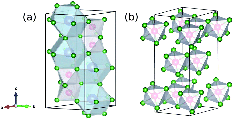 | ||
| Fig. 1 Schematic crystal structure of Cs3Bi2I9 (a) and BiI3 (b) that show layered octahedra that form a distorted cell. Vacancies are characteristic of this crystal structure. Bismuth atoms are shown in red, iodine in green, and cesium in blue. | ||
We use synchrotron-based X-ray spectroscopy methods to probe the electronic structure. The sensitivity to local coordination and associated hybridization can provide links between the structure and observed optical properties. The element-specific probe can show differences in the electronic structure induced by structural changes beyond the directly coordinating atoms. The interfacial energetics from photoemission spectroscopy and band structure calculations are used to interpret an energetically favorable transport at the TiO2/Cs3Bi2I9 interface. In order to study this directly, we use for the first time on bismuth halides the combination of hard X-ray photoelectron spectroscopy (HAXPES), partial fluorescence X-ray absorption spectroscopy (XAS, partial fluorescence yield mode), and resonant inelastic X-ray spectroscopy (RIXS). However, there are reports using HERFD-XAS and HAXPES on lead-based perovskite halides.32,33 By means of complementary X-ray spectroscopy techniques, the obtained data can be used to gain a detailed understanding of the electronic structure of our bismuth-halide based materials. The data are compared against density functional theory (DFT) calculations to reveal information on photovoltaic optical transitions and device design strategies.
2 Experimental
2.1 Thin film synthesis
Thin films of CsI, BiI3, and Cs3Bi2I9 were synthesized by a solution-based process through mixtures of appropriate precursor ratios. In short, CsI and BiI3 were dissolved in anhydrous N,N′-dimethylformamide (DMF) and dimethyl sulfoxide solution (7![[thin space (1/6-em)]](https://www.rsc.org/images/entities/char_2009.gif) :3) in a 3:2 molar ratio. The solution mixture was boiled at 100 °C for 3 hours inside a N2 fluxed dry box. Mesoscopic TiO2 (mTiO2) films were deposited on conducting FTO (fluorine-doped tin oxide) glass by spin coating at 3000 rpm for 30 s. The TiO2 paste was prepared by diluting Dyesol paste (30NR-T, particle size ≈ 30 nm) with ethanol in a 1:4 weight ratio. The mTiO2-coated glass was annealed on a hot plate at 100 °C for 30 min. The film thickness was ≈350 (±50 nm) as determined using a Dektak3 profiler. The bismuth halide perovskite precursor solutions were coated onto the TiO2/FTO substrate by spin-coating at 3500 rpm for 30 s, followed by annealing on a hot plate at 140 °C for 30 min in a dry air box (relative humidity less than 30%).
:3) in a 3:2 molar ratio. The solution mixture was boiled at 100 °C for 3 hours inside a N2 fluxed dry box. Mesoscopic TiO2 (mTiO2) films were deposited on conducting FTO (fluorine-doped tin oxide) glass by spin coating at 3000 rpm for 30 s. The TiO2 paste was prepared by diluting Dyesol paste (30NR-T, particle size ≈ 30 nm) with ethanol in a 1:4 weight ratio. The mTiO2-coated glass was annealed on a hot plate at 100 °C for 30 min. The film thickness was ≈350 (±50 nm) as determined using a Dektak3 profiler. The bismuth halide perovskite precursor solutions were coated onto the TiO2/FTO substrate by spin-coating at 3500 rpm for 30 s, followed by annealing on a hot plate at 140 °C for 30 min in a dry air box (relative humidity less than 30%).
2.2 Hard X-ray photoemission spectroscopy (HAXPES)
HAXPES was carried out at BESSY II (Helmholtz Zentrum Berlin) at the KMC-1 beamline using the HIKE end-station.34 A photon energy of 4000 eV is selected using first-order light from a Si (311) double-crystal monochromator (Oxford-Danfysik). Photoelectron spectra were recorded using a Scienta R4000 analyzer, optimized for high kinetic energies. At 4000 eV photon energy, a probing depth slightly below 20 nm is expected for the core levels reported here. The incident angle between the beam and the surface of the sample was ∼5°, while the photoelectrons were detected close to normal emission, ∼85°. The pressure in the analysis chamber was ∼10−8 mbar. The spectra presented were energy calibrated relative to the Au 4f7/2 core level binding energy which we set to 84.0 eV. The spectra were intensity calibrated using the most intense peak, if not stated otherwise. Intensity ratios presented between different core levels were calculated from the experimental results after correcting for photoionization cross-sections using database values.352.3 HERFD-XANES & RIXS
The High Energy Resolution Fluorescence Detected X-ray Absorption Near Edge Structure (HERFD-XANES) and Resonant Inelastic X-ray Scattering (RIXS) spectroscopy experiments were performed at the European Synchrotron Radiation Facility (ESRF).36,37 The HERFD-XANES (henceforth referred to as simply HERFD) spectra have been described previously.38 Bismuth L1 and L3 HERFD spectra were collected at the BM20 (ROBL) beamline using Si (880) and Ge (884) analyzers respectively. The HERFD-XANES spectra were recorded at the maximum of Lβ3 and Lα1 emission lines for Bi L1 and L3 absorption edges respectively. The overall resolution of HERFD data at the bismuth L1 and L3 edges is approximately 4.3 eV and 2.4 eV (including core-hole lifetime broadening) respectively. HERFD measurements at the iodine L1 edge were performed at the beamline ID26. Spectra were recorded at the maximum of the Lγ2,3 emission line (E = 5065 eV) with a resolution of 2.2 eV. RIXS spectra were recorded near the iodine L1 edge in the energy range of 5173–5196 eV with a resolution of 0.7 eV as determined from the full width at half maximum (FWHM) of the elastic peak. The energy in HERFD and RIXS was selected using the (331) reflection of three spherically bent Si crystal analyzers. The intensity was normalized to the incident flux measured using a photodiode. The spectrometer energy was calibrated using the elastic peak. Samples were positioned at 45° to the beam. A helium-filled bag was used to reduce absorption effects between the sample and crystal analyzer. Measurements were carried out on multiple spots on the samples to assess radiation damage. The spectra showed no detectable change within the acquisition time (5 min for HERFD and 25 min for RIXS).2.4 Computational
The calculations were carried out using an all electron full-potential linear muffin-tin orbital (FP-LMTO) method39 within the local density approximation (LDA) with spin–orbit coupling. The full-potential indicates that there are no geometrical constraints on the expansion of the density and potential (c.f. atomic sphere approximation (ASA) where spheres are used). Details on the implementation of the present FP-LMTO method can be found in ref. 39. It should be mentioned that we use an extended basis to eliminate or at least significantly reduce the solution dependence of the tail energies in the basis set, in the calculations. The FP-LMTO method used here is an all electron implementation meaning that no pseudo-potentials are used. The core electrons are treated explicitly by solving the Dirac equation and this process is part of the self-consistent loop, i.e. the core-density is relaxed at each iteration. Technical parameters such as the k-point grid and fast Fourier transform (FFT) mesh were set to give a converged electronic structure. In the present calculations the muffin-tin radii are maximized iteratively to cover 90% of the nearest neighbor distance. The input structures were taken from the literature on Cs3Bi2I9 (ref. 40) and BiI3.41 The calculated results are part of the electronic structure project, where the computational methods are also described in more detail.423 Results and discussion
3.1 Photoelectron spectroscopy
Fig. 2 shows overview spectra of a TiO2/Cs3Bi2I9 sample along with the precursors BiI3 and CsI to qualitatively follow the characteristic change in the electronic structure. All samples show their distinct core peaks, including some substrate peak contributions (Ti 2p and O 1s). Carbon and nitrogen peaks are negligible in intensity, indicating a minor contribution from surface contamination. Core-level intensity variations and the effect on the electronic signature will be discussed later. | ||
| Fig. 2 Survey spectra for precursor materials and the quasi-perovskite Cs3Bi2I9 measured at 4000 eV. The spectra are normalized to I 3d peaks. | ||
Core level spectra for Bi 4f, I 3d, and Cs 3d are presented in Fig. 3. The main contributions for Cs3Bi2I9 and BiI3 4f7/2 have peak maxima at 159.5 eV and 158.9 eV respectively (BiI3 Fig. S1†) a difference of 0.5 eV. Cs 4p (grey fill) and Bi 4f (blue fill) have an overlap near 161 eV. There is a small peak at lower binding energy from the main 4f7/2, indicating a metallic Bi (≈157.0 eV, brown fill) component present in both samples, likely an outcome of improper crystallization of thin films during synthesis. Metallic components in halide perovskites have been strongly linked to iodine deficiencies and vacancies,43 dissociation of precursor species during synthesis,44 and annealing processes.45,46 The primary bismuth peak shifted nearly 2 eV from the metallic, which is characteristic of Bi3+ oxidation, as reported in work by Park et al.17 The core-level Bi 4f7/2 maxima for Cs3Bi2I9 and BiI3 differ by 0.54 eV. The FWHM difference can be attributed to disorder in the Cs3Bi2I9 sample since all other contributions to the Bi 4f linewidth should be the same. Slight differences in the environment of the Bi from site to site (e.g. as vacancies, substitutional disorder, and structural variations) result in small changes in the binding energy position which contribute to an overall core-level broadening. The small modifications in the core level width and position can be rationalized in terms of a higher charge density around the Bi atom for the face-sharing octahedra for Cs3Bi2I9 compared to the edge-sharing octahedra for BiI3. The I 3d core level peak is at a binding energy of 619.5 eV, 619.4 eV, and 619.5 eV for the Cs3Bi2I9, BiI3, and CsI samples respectively. The spin–orbit splitting is 11.5 eV in the I 3d3/2 level for all samples, and the binding energy positions, indicating a monovalent iodine atom in each of the samples with a similar coordination.
 | ||
| Fig. 3 (a) Core level peaks for bismuth 4f for Cs3Bi2I9 and BiI3. The Bi 4f spectrum for Cs3Bi2I9; experimental (red markers) and fitted spectra (black line) overlap with Cs 4p (grey fill) at around ≈161 eV. BiI3 peak, shown with green markers, shows a small shift towards lower binding energy and a narrower width than Cs3Bi2I9. The spectra are normalized to Bi 4f7/2 peak intensity. The gold fill shows the Bi metallic component. (b) I 3d spectra (right) show a narrower width for BiI3 with little modification in binding energy positions. (c) Cs 3d core level spectra. | ||
An approximate estimation of the material stoichiometry can be made using the relative intensities of the experimental core levels. In such a calculation one needs to take into account the differential cross-sections and angle between the photoelectrons and the polarization direction of the X-rays.47,48 The stoichiometry estimation for I/Bi in Cs3Bi2I9 is 4.34, reasonably close to the expected value of 4.5 when using Bi 5d and I 4d core levels. The cesium to iodide is 2.7 using Cs 4d and I 4d, also expected for Cs3Bi2I9. The experimental stoichiometry for BiI3 is 2.9, close to the expected value of 3, and finally 0.98 for CsI as expected. The matching between the experimental values and expected values from the stoichiometry supports the high quality of the samples. For these materials, effects from surface segregation or reconstruction are limited due to the bulk probe of the high photon energies.
3.2 X-ray absorption & emission spectroscopy
The HERFD-XANES helps to reduce the core-hole broadening of XANES spectra by monitoring the specific emission line as scanning across an absorption edge.49 This second-order process mitigates the inherent core-hole lifetime broadening. Fig. 4 shows the normalized (normalized at the higher energy side of the spectrum) Bi L1 (Fig. 4a) and L3 (Fig. 4b) absorption edges of Cs3Bi2I9 along with BiI3. The edge positions for the Bi L1 edges for the two samples studied are practically equivalent (Cs3Bi2I9 L1: 16388.5 eV, BiI3 L1: 16388.9 eV, determined by the maximum of the second derivative), as expected for samples with the same formal Bi valence state (Bi3+). The strong peak near ∼16395 eV is a so-called ‘white line’ feature and is ascribed to transitions from 2s → 6p states, just above the Fermi energy (EF). High-energy structures, i.e. features a few eV after the main absorption line, are structures due to multiple scattering effects.50 The L3 edge position in Fig. 4b also shows a 3+ formal charge with small fine structure variations amongst the two samples. The L3 absorption edge positions for Cs3Bi2I9 and BiI3 are 13413.9 and 13413.7 eV respectively. The key spectral changes in the Bi L3 spectrum are shown in the difference spectra (blue fill) between BiI3 and Cs3Bi2I9 respectively and specifically shown in the pre-edge feature (inset Fig. 4b). Since the lower energy side of the spectrum is expected to come from transitions from occupied 2p to unoccupied anti-bonding 6s states, these differences show the increase in available anti-bonding 6s states for Cs3Bi2I9, representative of a slight change in I p–Bi s hybridization. The difference in the relative intensity and positions of the spectra is attributed to different overlaps between the metal cation and iodine, as an effect of the distances between I and Bi is smaller for Cs3Bi2I9 than for BiI3 (see Table S1 in ESI†). From these two spectra, we suggest that the p character in the conduction band for both samples stays relatively similar with only small differences in the s character as seen from the difference spectra. Since the unoccupied bismuth states of BiI3 and Cs3Bi2I9 show large similarities, it seems appropriate to probe the iodide occupied and unoccupied states to further distinguish the electronic structure.
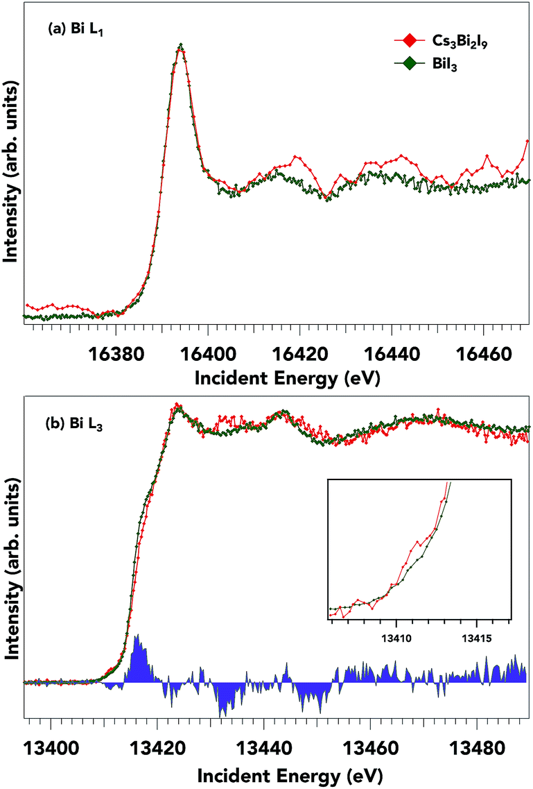 | ||
| Fig. 4 (a) Bismuth L1 and (b) bismuth L3 HERFD-XANES spectrum for Cs3Bi2I9 and BiI3. Although the Bi L1 edge has a low signal-to-noise ratio, the spectrum can still be used to describe the chemical state. The L3 spectrum is sensitive to changes in the crystal structure, and shows slight differences in Bi 6s2 states as highlighted by the difference spectra (blue fill) and the inset figure. | ||
HERFD-XANES spectra at the Iodine L1 edge for Cs3Bi2I9 and its precursors are shown in Fig. 5 along with the projected electronic density of states (DOS) of Cs3Bi2I9 using the LDA functional with SOC. The absorption for the iodine L1 edge is shown in Fig. 5a. The partial fluorescence yield was detected using the maximum of the Lγ2,3 (5065 eV) emission line. As outlined previously, the advantage of this setup is that the width of the spectral features is no longer limited by the final state 2s core-hole lifetime but by the smaller 4p3/2 core-hole lifetime. All three samples show distinct spectral features and characters, a consequence of different coordination and displacement of iodine atoms in the unit cell. Although both bismuth compounds show formal Bi3+, the sharper white line and higher intensity for BiI3 could be interpreted as a more localized charge distribution around the I ions in Cs3Bi2I9. This narrowing is likely due to the interlayer nature of the BiI3 crystal structure. The edge positions (here defined as the zero crossing of the second derivative) for BiI3, Cs3Bi2I9, and CsI span an energy range of 4.2 eV. As the bandgap of the three compounds varies greatly between BiI3 (Eg: 1.8 eV), Cs3Bi2I9 (2.2 eV), and CsI (6.2 eV), the shift to higher energy for unoccupied iodine states correlates with the observed increase in the bandgap. In contrast to the Bi L1 and L3 HERFD-XANES spectra, where the Bi atom occupies a similar coordination in the octahedra, the iodine atoms are displaced in each compound with its own symmetry. These specific crystal structure parameters are directly responsible for the varying features in the spectra. The lack of strong pre-edge features suggests that the counter cation (Cs+) is strongly ionic and no mixing exists with I p states at the edge of the conduction band. Feature a in the absorption spectrum for Cs3Bi2I9 and BiI3 is associated with excitations to the first unoccupied p states of iodine, which has covalent character with bismuth s and p states. The subsequent maxima at points (b) and (c) for Cs3Bi2I9 and BiI3 are transitions to hybridized I p and Bi p with the admixture from Cs d states, as seen in the calculated DOS on their right panel for Cs3Bi2I9 and BiI3. Cs d states contribute mainly in the post-edge region; therefore the conduction band minimum is strictly determined from Bi/I states.
 | ||
| Fig. 5 HERFD-XAS iodine L1 edge (a) reflects the unoccupied iodine p states in the conduction band and sensitivity to local coordination. The projected DOS in the CB is shown for Cs3Bi2I9 (b) and BiI3 (c). | ||
In Fig. 6, RIXS spectra at the I L1 emission on an energy loss scale are shown. RIXS is highly sensitive to the ligands coordinating to a metal and therefore is an adept tool for probing the ligand coordination environment and valence states.51 Here, an I 2s (core-electron) is resonantly excited at 5.190 keV for Cs3Bi2I9 and BiI3 and at 5.195 keV for CsI. The spectrometer scans in an energy window that can only be a radiative decay of levels containing I 5p character, characteristic of the highest occupied orbital. In this case, core-hole effects are negligible due to a high degree of delocalization of I 5p states. The observed main peak around 4 eV energy loss is from a mix of I 5p and Bi 6s, p states. There are no distinguishable features that indicate hybridization with the Cs cation, which is expected since its shallow valence levels do not participate in covalent bonding as shown in the next section. Since the excitation energy for the RIXS spectra was set to the first structure in the I L1 XAS spectra, the energy difference between the elastic peak and the onset of the inelastic structures on the energy loss scale correlates with the size of the band gap in these compounds. Therefore, the shift of such an onset to a lower energy loss by 0.4 eV in BiI3 as compared with Cs3Bi2I9 indicates a small band gap in the former. This information can provide insight into the changes of I p states, and how they ultimately affect the band gap. These results also suggest that the Cs cation has no direct effect on varying the band gap of Cs3Bi2I9, as was shown by DFT calculations recently.52
 | ||
| Fig. 6 The RIXS spectra represent contributions of occupied I 5p states in the valence band for the three materials. | ||
The experimental valence band for the three samples on mTiO2 and valence DFT calculations for Cs3Bi2I9 and BiI3 are shown in Fig. 7. The overall spectral shape of Cs3Bi2I9 has a structure that follows the characteristics of that of the precursors, with modification in the valence band edge position in between the low bandgap BiI3 and high bandgap CsI. The high photon energy of 4000 eV provides a relatively bulk sensitive probe. The ionization cross-sections for Bi 5p and 6s states are nearly the same as that of I 5p at 4000 eV. The doublet peak near ∼12 eV corresponds to Cs 5p orbitals, states that do not participate in bonding. The calculated partial and total density of states along with experimental spectra in the valence band are presented in Fig. 7b. The spectra are dominated by I 5p states extending from the valence band onset to about 6–8 eV in binding energy. The data are in general agreement with the calculated spectra presented here; however small discrepancies are common when comparing experimental photoemission to that of DFT calculations. The plot shows the calculated contributions of I 5p and Bi 6s/5p states, along with the total calculated DOS and experimental photoemission data. The DFT results are in close agreement with other DFT calculations using the Generalized Gradient Approximation (GGA) and the projector-augmented wave (PAW) formalism.18,19 The Cs contribution to the VB is near 10 eV, and therefore does not participate in bonding with the frontier states of bismuth and iodine. I p states hybridize to a small degree with Bi lone pair s states towards the edge of the valence band. The mixing of ligand and lone pair states is crucial in producing asymmetric electron density in the Bi ion.53 This mixing produces filled bonding and anti-bonding states that give its ‘defect-tolerant’ properties within the valence band.
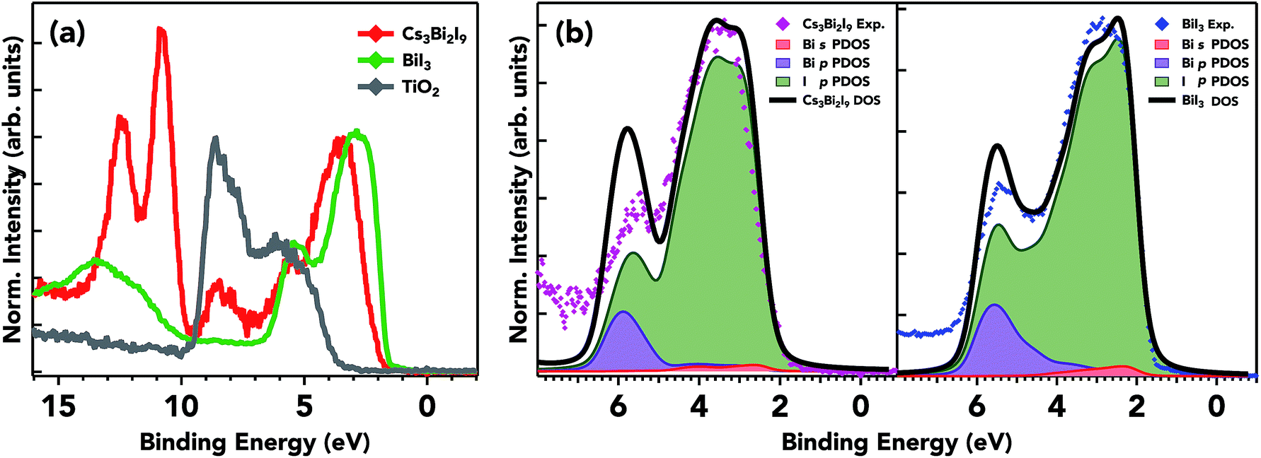 | ||
| Fig. 7 Valence band spectra for the three samples at 4000 eV (a) and calculated VB pDOS for Cs3Bi2I9 and BiI3 (b). DFT calculations showing the partial and total density of states along with experimental spectra in the valence band. The principal differences in the two samples are the positions and weight of the Bi s states in the VB. The I p character is almost the same in terms of spectral weight and features. | ||
3.3 Valence band structure and interfacial energetics
The determination of experimental band positions is a critical step in the evaluation of the material electronic properties and their role in photovoltaic design. The relative position of the three materials in relation to the conduction band minimum (CBM) of titania is imperative for electron transfer and voltage loss in the device. An approximation of the valence band maximum (VBM) can be interpreted by taking the linear extrapolation on the low binding energy end of the VB HAXPES spectrum, in accordance with the location of the Fermi level set by the gold Au 4f7/2 spectra as show in Fig. 8. The band gap is derived from Tauc plots (ESI: Fig. S2†) and is used to determine the CB minimum (CBM). The energy difference of the valence band edges between TiO2 and the halide compounds is −1.73 eV, −1.93 eV, and −1.05 for Cs3Bi2I9, BiI3, and CsI respectively. From this representation, the band edges of Cs3Bi2I9 and BiI3 are well matched for the electron transport material mTiO2 and favorable for electron transfer without significant loss. The relevant data on the band positions of the conduction band minimum (CBM) and valence band maximum (VBM) provide a means to determine the material requirements for appropriate interfacial layers in solar cells. This shows the efficacy of using HAXPES in order to determine relative band-offsets in light harvesting materials.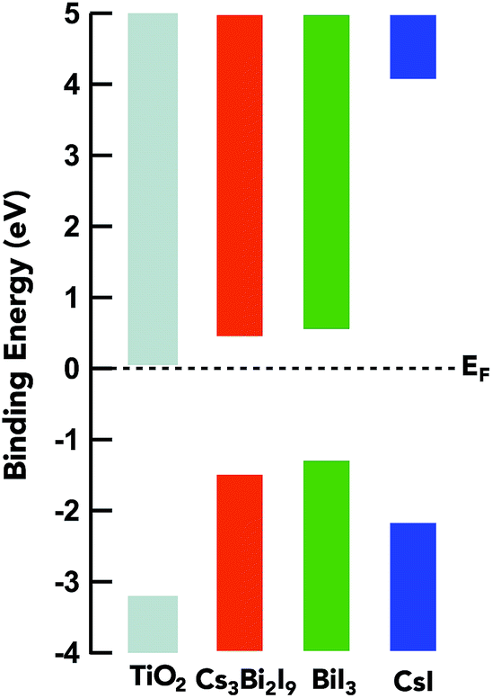 | ||
| Fig. 8 The energy level alignment between mTiO2 and the samples measured using HAXPES measurements. Optical band gaps for the samples are estimated from UV-Vis absorption spectra. | ||
4 Conclusions
In summary, we used several X-ray spectroscopic techniques along with support from DFT calculations to investigate the electronic structure and band energetics of Cs3Bi2I9, BiI3, and CsI. HERFD-XAS at the Bi L1 and L3 edges shows very similar local coordination for Bi atoms in both Cs3Bi2I9 and BiI3, with a modest increase in available Bi s in the CB for Cs3Bi2I9. The complimentary RIXS data also show a similar VB profile of the highest occupied p states, with changes only in the position of I 5p occupied states. HAXPES data show a similar spectral profile towards the band edge, and calculations revealed very similar mixing of I p states and Bi s and Bi p states. The primary significance was the position of the VBM, which is used to construct the interfacial profile against a mTiO2 interface to show a favorable electronic transport in optoelectronic applications. These findings demonstrate the utility of hard X-ray spectroscopy in identifying detailed electronic structures and their use in solar harvesting devices.Conflicts of interest
There are no conflicts to declare.Acknowledgements
We acknowledge financial support from the Swedish Research Council (2014-6019, 2016-4524), the Swedish Energy Agency (P43549-1), the Swedish Foundation for Strategic Research (15-0130), the Wallenberg Foundation (2012.0031), and the StandUP for Energy. HZB and ESRF are acknowledged for the allocation of synchrotron radiation beamtime. The computations were performed on resources provided by the Swedish National Infrastructure for Computing (SNIC) at the Swedish National Supercomputer Center (NSC).Notes and references
- M. M. Lee, J. Teuscher, T. Miyasaka, T. N. Murakami and H. J. Snaith, Science, 2012, 338, 643–647 CrossRef CAS PubMed.
- H.-S. Kim, C.-R. Lee, J.-H. Im, K.-B. Lee, T. Moehl, A. Marchioro, S.-J. Moon, R. Humphry-Baker, J.-H. Yum, J. E. Moser, M. Grätzel and N.-G. Park, Sci. Rep., 2012, 2, 591 CrossRef PubMed.
- J. Luo, J.-H. Im, M. T. Mayer, M. Schreier, M. K. Nazeeruddin, N.-G. Park, S. D. Tilley, H. J. Fan and M. Gratzel, Science, 2014, 345, 1593–1596 CrossRef CAS PubMed.
- Z.-K. Tan, R. S. Moghaddam, M. L. Lai, P. Docampo, R. Higler, F. Deschler, M. Price, A. Sadhanala, L. M. Pazos, D. Credgington, F. Hanusch, T. Bein, H. J. Snaith and R. H. Friend, Nat. Nanotechnol., 2014, 9, 1–6 CrossRef PubMed.
- G. Xing, N. Mathews, S. S. Lim, N. Yantara, X. Liu, D. Sabba, M. Grätzel, S. Mhaisalkar and T. C. Sum, Nat. Mater., 2014, 13, 476–480 CrossRef CAS PubMed.
- O. A. Jaramillo-Quintero, R. S. Sánchez, M. Rincón and I. Mora-Sero, J. Phys. Chem. Lett., 2015, 6, 1883–1890 CrossRef CAS PubMed.
- F. Zhang, H. Zhong, C. Chen, X.-g. Wu and X. Hu, ACS Nano, 2015, 9, 4533–4542 CrossRef CAS PubMed.
- X. Y. Chin, D. Cortecchia, J. Yin, A. Bruno and C. Soci, Nat. Commun., 2015, 6, 7383 CrossRef CAS PubMed.
- N. J. Jeon, J. H. Noh, Y. C. Kim, W. S. Yang, S. Ryu and S. I. Seok, Nat. Mater., 2014, 13, 897–903 CrossRef CAS PubMed.
- T.-b. Song, Q. Chen, H.-P. Zhou, C. Jiang, H.-H. Wang, Y. Yang, Y. Liu and J. You, J. Mater. Chem. A, 2015, 3, 9032–9050 CAS.
- P. Fan, D. Gu, G.-X. Liang, J.-T. Luo, J.-L. Chen, Z.-H. Zheng and D.-P. Zhang, Sci. Rep., 2016, 6, 29910 CrossRef CAS PubMed.
- L. K. Ono, M. R. Leyden, S. Wang and Y. Qi, J. Mater. Chem. A, 2016, 4, 6693–6713 CAS.
- S. M. Jain, B. Philippe, E. M. J. Johansson, B.-w. Park, H. Rensmo, T. Edvinsson and G. Boschloo, J. Mater. Chem. A, 2016, 4, 2630–2642 CAS.
- A. Babayigit, D. Duy Thanh, A. Ethirajan, J. Manca, M. Muller, H.-G. Boyen and B. Conings, Sci. Rep., 2016, 6, 18721 CrossRef CAS PubMed.
- T. Leijtens, G. E. Eperon, N. K. Noel, S. N. Habisreutinger, A. Petrozza and H. J. Snaith, Adv. Energy Mater., 2015, 5, 1500963 CrossRef.
- B. Philippe, B. W. Park, R. Lindblad, J. Oscarsson, S. Ahmadi, E. M. J. Johansson and H. Rensmo, Chem. Mater., 2015, 27, 1720–1731 CrossRef CAS.
- B.-W. Park, B. Philippe, X. Zhang, H. Rensmo, G. Boschloo and E. M. J. Johansson, Adv. Mater., 2015, 27, 6806–6813 CrossRef CAS PubMed.
- A. J. Lehner, D. H. Fabini, H. A. Evans, C. A. Hébert, S. R. Smock, J. Hu, H. Wang, J. W. Zwanziger, M. L. Chabinyc and R. Seshadri, Chem. Mater., 2015, 27, 7137–7148 CrossRef CAS.
- M. Pazoki, M. B. Johansson, H. Zhu, P. Broqvist, T. Edvinsson, G. Boschloo and E. M. J. Johansson, J. Phys. Chem. C, 2016, 120, 29039–29046 CAS.
- A. T. Lintereur, W. Qiu, J. C. Nino and J. Baciak, Nucl. Instrum. Methods Phys. Res., Sect. A, 2011, 652, 166–169 CrossRef CAS.
- P. M. Johns, J. E. Baciak and J. C. Nino, Appl. Phys. Lett., 2016, 109, 092105 CrossRef.
- R. E. Brandt, R. C. Kurchin, R. L. Z. Hoye, J. R. Poindexter, M. W. B. Wilson, S. Sulekar, F. Lenahan, P. X. T. Yen, V. Stevanovic, J. C. Nino, M. G. Bawendi and T. Buonassisi, J. Phys. Chem. Lett., 2015, 6, 4297–4302 CrossRef CAS PubMed.
- A. Farzaneh, M. R. Abdi, K. R. E. Saraee, M. Mostajaboddavati and A. Quaranta, Opt. Mater., 2016, 55, 22–26 CrossRef CAS.
- G. Papavassiliou, I. Koutselas, A. Terzis and M.-H. Whangbo, Solid State Commun., 1994, 91, 695–698 CrossRef CAS.
- A. Walsh, D. J. Payne, R. G. Egdell and G. W. Watson, Chem. Soc. Rev., 2011, 40, 4455–4463 RSC.
- R. E. Brandt, V. Stevanović, D. S. Ginley and T. Buonassisi, MRS Commun., 2015, 5, 1–11 CrossRef.
- L. Y. Huang and W. R. L. Lambrecht, Phys. Rev. B: Condens. Matter Mater. Phys., 2013, 88, 1–12 Search PubMed.
- A. M. Ganose, K. T. Butler, A. Walsh and D. O. Scanlon, J. Mater. Chem. A, 2016, 4, 2060–2068 CAS.
- B. Chabot and E. Parthe, Acta Crystallogr., Sect. B: Struct. Crystallogr. Cryst. Chem., 1978, 34, 645–648 CrossRef.
- A. Jorio, R. Currat, D. Myles, G. McIntyre, I. Aleksandrova, J. Kiat and P. Saint-Grégoire, Phys. Rev. B: Condens. Matter Mater. Phys., 2000, 61, 3857–3862 CrossRef CAS.
- R. T. Poole, J. G. Jenkin, J. Liesegang and R. C. G. Leckey, Phys. Rev. B: Solid State, 1975, 11, 5179–5189 CrossRef CAS.
- B. Philippe, M. Saliba, J. P. Correa-Baena, U. B. Cappel, S. H. Turren-Cruz, M. Grätzel, A. Hagfeldt and H. Rensmo, Chem. Mater., 2017, 29, 3589–3596 CrossRef CAS.
- W. S. Drisdell, L. Leppert, C. M. Sutter-Fella, Y. Liang, Y. Li, Q. P. Ngo, L. F. Wan, S. Gul, T. Kroll, D. Sokaras, A. Javey, J. Yano, J. B. Neaton, F. M. Toma, D. Prendergast and I. D. Sharp, ACS Energy Lett., 2017, 2, 1183–1189 CrossRef.
- M. Gorgoi, S. Svensson, F. Schäfers, G. Öhrwall, M. Mertin, P. Bressler, O. Karis, H. Siegbahn, A. Sandell, H. Rensmo, W. Doherty, C. Jung, W. Braun and W. Eberhardt, Nucl. Instrum. Methods Phys. Res., Sect. A, 2009, 601, 48–53 CrossRef CAS.
- J. H. Scofield, UCRL-51326: Theoretical Photoionization Cross Sections from 1 to 1500 keV, University of California-Livermore, 1973, vol. 257, p. 374 Search PubMed.
- C. Gauthier, V. A. Solé, R. Signorato, J. Goulon and E. Moguiline, J. Synchrotron Radiat., 1999, 6, 164–166 CrossRef CAS PubMed.
- K. O. Kvashnina and A. C. Scheinost, J. Synchrotron Radiat., 2016, 23, 836–841 CrossRef CAS PubMed.
- A. J. Atkins, C. R. Jacob and M. Bauer, Chem.–Eur. J., 2012, 18, 7021–7025 CrossRef CAS PubMed.
- J. M. Wills, O. Eriksson, M. Alouani and D. L. Price, Electronic Structure and Physical Properties of Solids: the Uses of the LMTO Method, Springer-Verlag Berlin Heidelberg, 2000 Search PubMed.
- O. Lindqvist, G. Johansson, F. Sandberg and T. Norin, Acta Chem. Scand., 1968, 22, 2943–2952 CrossRef CAS.
- J. Trotter and T. Zobel, Z. Kristallog. Krist., 1966, 123, 67–72 CAS.
- C. Ortiz, O. Eriksson and M. Klintenberg, Comput. Mater. Sci., 2009, 44, 1042–1049 CrossRef CAS.
- W. Zhang, S. Pathak, N. Sakai, T. Stergiopoulos, P. K. Nayak, N. K. Noel, A. A. Haghighirad, V. M. Burlakov, D. W. DeQuilettes, A. Sadhanala, W. Li, L. Wang, D. S. Ginger, R. H. Friend and H. J. Snaith, Nat. Commun., 2015, 6, 10030 CrossRef CAS PubMed.
- W. Xu, L. Liu, L. Yang, P. Shen, B. Sun and J. A. McLeod, Nano Lett., 2016, 16, 4720–4725 CrossRef CAS PubMed.
- G. Sadoughi, D. E. Starr, E. Handick, S. D. Stranks, M. Gorgoi, R. G. Wilks, M. Bär and H. J. Snaith, ACS Appl. Mater. Interfaces, 2015, 7, 13440–13444 CAS.
- B. Philippe, B. W. Park, R. Lindblad, J. Oscarsson, S. Ahmadi, E. M. J. Johansson and H. Rensmo, Chem. Mater., 2015, 27, 1720–1731 CrossRef CAS.
- M. Trzhaskovskaya, V. Nefedov and V. Yarzhemsky, At. Data Nucl. Data Tables, 2001, 77, 97–159 CrossRef CAS.
- M. Trzhaskovskaya, V. Nefedov and V. Yarzhemsky, At. Data Nucl. Data Tables, 2002, 82, 257–311 CrossRef CAS.
- M. Bauer, Phys. Chem. Chem. Phys., 2014, 16, 13827–13837 RSC.
- J. J. Rehr, Rev. Mod. Phys., 2000, 72, 621–654 CrossRef CAS.
- E. R. Hall, C. J. Pollock, J. Bendix, T. J. Collins, P. Glatzel and S. Debeer, J. Am. Chem. Soc., 2014, 136, 10076–10084 CrossRef CAS PubMed.
- X. Huang, S. Huang, P. Biswas and R. Mishra, J. Phys. Chem. C, 2016, 120, 28924–28932 CAS.
- A. Walsh, G. W. Watson, D. J. Payne, R. G. Edgell, J. Guo, P.-A. Glans, T. Learmonth and K. E. Smith, Phys. Rev. B: Condens. Matter Mater. Phys., 2006, 73, 235104 CrossRef.
Footnote |
| † Electronic supplementary information (ESI) available: A table for the selected distances in the crystal structure of Cs3Bi2I9 and BiI3, HAXPES Bi 4f core level spectra, and UV-Vis experimental Tauc plots (PDF). See DOI: 10.1039/c8ta00947c |
| This journal is © The Royal Society of Chemistry 2018 |