Exploring the transposition effects on the electronic and optical properties of Cs2AgSbCl6via a combined computational-experimental approach†
Received
15th November 2017
, Accepted 27th December 2017
First published on 28th December 2017
Abstract
The electronic and optical properties of perovskites are related to the local structures of the compounds and define their functional applications. Herein we have prepared a double perovskite Cs2AgSbCl6, which crystallized in the cubic structure with the space group Fm-3m and the material is found to have a varied band gap associated with different body colors. The anti-site defect model was established to investigate transposition influence on the optical and electronic properties of the double-perovskite Cs2AgSbCl6, and the proposed model clearly explained the as-observed variable body color. Cs2AgSbCl6 perovskite has a high decomposition temperature and is stable upon prolonged exposure to air and moisture, which emphasize its potential in the field of photovoltaic absorbers and optoelectronic applications.
1 Introduction
In a remarkably short period of time, Pb-based halide perovskites have launched a new paradigm in the area of solution processable solar cells, surpassing polycrystalline and thin-film silicon photovoltaics, and achieving record power conversion efficiencies above 22%.1–3 The most extensively studied materials by far are the APbX3 perovskites where A is an alkyl ammonium cation CH3NH3+ or Cs+ ion, and X is a halide ion (Cl−, Br−, I−).4,5 Despite their extremely outstanding solar cell performance, the toxicity of lead and the chemical instability of the lead halide perovskites impede their commercialization in the future.6 Given these limitations, searching for new air-stable and nontoxic lead-free halide perovskites via rational design is one of the key challenges to be addressed in the field of perovskite optoelectronics.7
There are different structural design principles adopted in the search for potential Pb-replacements. One straightforward idea to solve the Pb toxicity issue involves replacing Pb2+ by Sn2+ from the same periodic group, but the chemical instability of Sn2+ and poor performance give rise to limitations for their further use.8,9 Another promising approach to replace Pb is substitution by more stable cations, Bi3+ or Sb3+, which is isoelectronic with Pb2+. However, the change of divalent to trivalent metal oxidation state implies a need for vacancies on the metal site and therefore lower dimensional structures and wider band gaps for the resulting A3M2VX9 (A = K+, Cs+, Rb+, [NH4]+ and [CH3NH3]+; V = vacancy; M = Bi and Sb; X = Cl, Br and I).10,11
Nevertheless, the fact is that there are only a few bivalent or trivalent cations alternative to Pb2+ that form stable and non-toxic perovskites.12 Therefore, another viable route is combination with a monovalent and a trivalent cation together, which leads to the formation of a double perovskite structure with the basic formula A2B′B′′X6 (A = CH3NH3+ or Cs+; B′ = Na+, Cu+ or Ag+; B′′ = Bi3+, Sb3+ or In3+; X = Cl−, Br−, or I−).13–15 The double perovskites were first investigated in the 1970s, initially in the context of ferroelectrics.16 Recently, in the light of the intense interest in halide perovskites, our group reported Cs2AgInCl6 with a band gap of 3.23 eV and it can be stable for several weeks in air.17 Later, Tran et al. successfully controlled the direct vs. indirect nature of the band gap in halide perovskites in Cs2AgSb1−xInxCl6 solid solution.18 Herein, we adopted a hydrothermal method to grow pure Cs2AgSbCl6 crystals with a varied band gap, and we established an anti-site defect model by density functional theory (DFT) to investigate transposition influence on the electronic and optical properties of the double-perovskite Cs2AgSbCl6. This site-equal transposition, which easily occurred during the experimental process, did not change the atomic ratio and had a big influence on the band gap. Moreover, the Cs2AgSbCl6 crystal was found to be stable in air for several weeks and has a high decomposition temperature. This material shows great potential for optoelectronics application via further band gap engineering.
2 Experimental section
2.1 Materials and preparation
All the chemicals were commercially purchased and used without further purification. Crystals of Cs2AgSbCl6 were synthesized by the hydrothermal method in a stainless steel Parr autoclave using 2.4 mmol CsCl (99.99%, Aladdin), 1.2 mmol AgCl (99.5%, Aladdin) and 1.2 mmol SbCl3 (99.9%, Aladdin) in a certain amount (0.5 mL to 1.5 mL) of HCl acid solution (99.5%, Beijing Chemical Works). The powders with colors from yellow to near black by alternating the volume of the added HCl were precipitated from solution during the hydrothermal reaction at 453 K over 12 h. This solid product was filtered out, washed with ethanol and finally dried under reduced pressure overnight.
2.2 Characterization
Powder X-ray diffraction (XRD) measurements were conducted on a D8 Advance diffractometer (Bruker Corporation, Germany) operating at 40 kV and 40 mA with Cu Kα radiation (λ = 0.15406 Å), and the scanning rate was fixed at 4° min−1. The powder diffraction pattern for Rietveld analysis was collected with the same diffractometer. The step size of 2θ was 0.016°, and the counting time was 1 s per step. Rietveld refinement was performed by using TOPAS 4.2 software.19 The morphology and crystalline size of the Cs2AgSbCl6 samples were determined by scanning electron microscopy (SEM, JEOL JSM-6510). The diffuse reflectance spectra were measured on a UV-Vis-NIR spectrophotometer (SHIMADZU UV-3600) supplied with an integrating sphere. BaSO4 was used as a reference standard. Thermogravimetric analysis and differential scanning calorimetry (TG-DSC) were performed on a Setaram Labsys Evo at 10 °C min−1 in an argon flow from room temperature to 1000 °C.
2.3 Computational methods
The band structure of Cs2AgSbCl6 is calculated by first-principles calculations using density functional theory (DFT), as implemented in the Vienna ab initio simulation package (VASP) code.20,21 The projector augmented wave (PAW) potential method was used to describe the interactions between ions and electrons. The exchange–correlation interactions between electrons were treated within the generalized gradient approximation (GGA-PBE).22,23 The plane wave cut-off energy of 520 eV was used for all total energy calculations and structure optimization and the K-point meshes for different structures were generated according to the Monkhorst–Pack scheme24 for the Brillouin zones. To reduce the self-interaction error of DFT in band gap calculations, we used the Heyd–Scuseria–Ernzerhof (HSE) hybrid functional approach25 to evaluate the band gap and to compare with the PBE functional approach.
3 Results and discussion
3.1 Crystalline phase and morphology
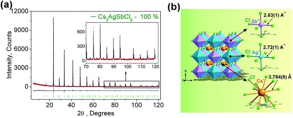
Fig. 1a displays the observed (black), calculated (red), and the difference (grey) XRD profiles for the Rietveld refinement of Cs2AgSbCl6. It is found that all peaks of the patterns were successfully indexed to a cubic cell (Fm-3m) with parameters close to Cs2AgAuCl6 (elpasolite-type structure).26 In comparison, the site of Au ion in Cs2AgAuCl6 is occupied by Sb. Cs2AgSbCl6 belongs to the as-expected lead-free double perovskite family, crystallizes in the cubic unit cell with the space group Fm-3m, and cell parameters, a = 10.70093 (6), Z = 4. The refinements of Cs2AgSbCl6 were stable, and the main parameters of processing and refinement with low R-factors are provided in Table 1. The crystallographic information file (CIF) of Cs2AgSbCl6 is given in the ESI.† Further details of the crystal structure may be obtained from Fachinformationszentrum Karlsruhe, 76344 Eggenstein-Leopoldshafen, Germany (fax: (+49)7247-808-666; E-mail: crystdata@fiz-karlsruhe.de; http://www.fiz-karlsruhe.de/request_for_deposited_data.html on quoting the deposition numbers: CSD-433743).
 |
| | Fig. 1 (a) Observed (black), calculated (red), and difference (gray) XRD profiles for the refinement of the Cs2AgSbCl6 sample using the Rietveld method. (b) Crystal structure of Cs2AgSbCl6 and coordination environments for Sb3+, Ag+, and Cl− are given. | |
Table 1 Main parameters of processing and refinement of the Cs2AgSbCl6 sample
| Compound |
Cs2AgSbCl6 |
| Sp.Gr. |
Fm-3m |
|
a, Å |
10.70093 (6) |
|
V, Å3 |
1225.36 (2) |
|
Z
|
4 |
| 2θ-interval, ° |
5–120 |
|
R
wp, % |
11.57 |
|
R
p, % |
8.39 |
|
R
exp, % |
9.40 |
|
χ
2
|
1.23 |
|
R
B, % |
2.01 |
A visualization of the double perovskite structure is presented in Fig. 1b, and the fractional atomic coordinates are also given in Table 2. Cs2AgSbCl6 exhibits a 3-dimensional framework of corner-sharing alternating octahedra of [AgCl6] and [SbCl6], with Cs+ cations located in the cavities formed between the octahedra, resulting in a double cell, i.e., elpasolite K2NaAlF6 structure, as also observed in Cs2AgInCl6.17 The Sb–Cl bond length (2.63(1) Å) is slightly shorter than that of Ag–Cl (2.72(1) Å), as expected.
Table 2 Fractional atomic coordinates and isotropic displacement parameters (Å2) of Cs2AgSbCl6
|
|
x
|
y
|
z
|
B
iso
|
| Cs |
1/4 |
1/4 |
1/4 |
2.71 (9) |
| Ag |
1/2 |
1/2 |
1/2 |
1.6 (1) |
| Sb |
0 |
0 |
0 |
1.1 (1) |
| Cl |
0.2456 (11) |
0 |
0 |
3.1 (1) |
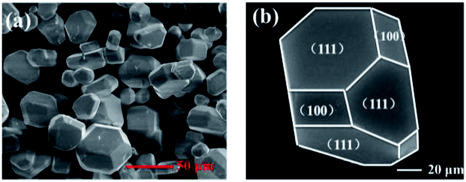
Fig. 2a shows the typical SEM images of the as-prepared Cs2AgSbCl6 microcrystals, which are comprised of numerous uniform rhombic dodecahedron particles with a size of 15–60 μm. A closer observation of the magnified images for one microcrystal (Fig. 2b) demonstrates that the rhombic dodecahedron shows the typical fcc-crystal features, a tetradecahedral crystallization habit forming a truncated octahedral. Besides, the exhibited facets of Cs2AgSbCl6 were determined to be (100) and (111). Additionally, the well faceted microcrystal shapes generally indicate the high structural quality of the powder product, as obtained for several other compounds.27–29
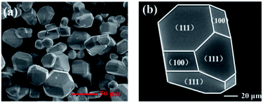 |
| | Fig. 2 (a) Typical SEM images of Cs2AgSbCl6 crystals, (b) one representative microcrystal showing different facets. | |
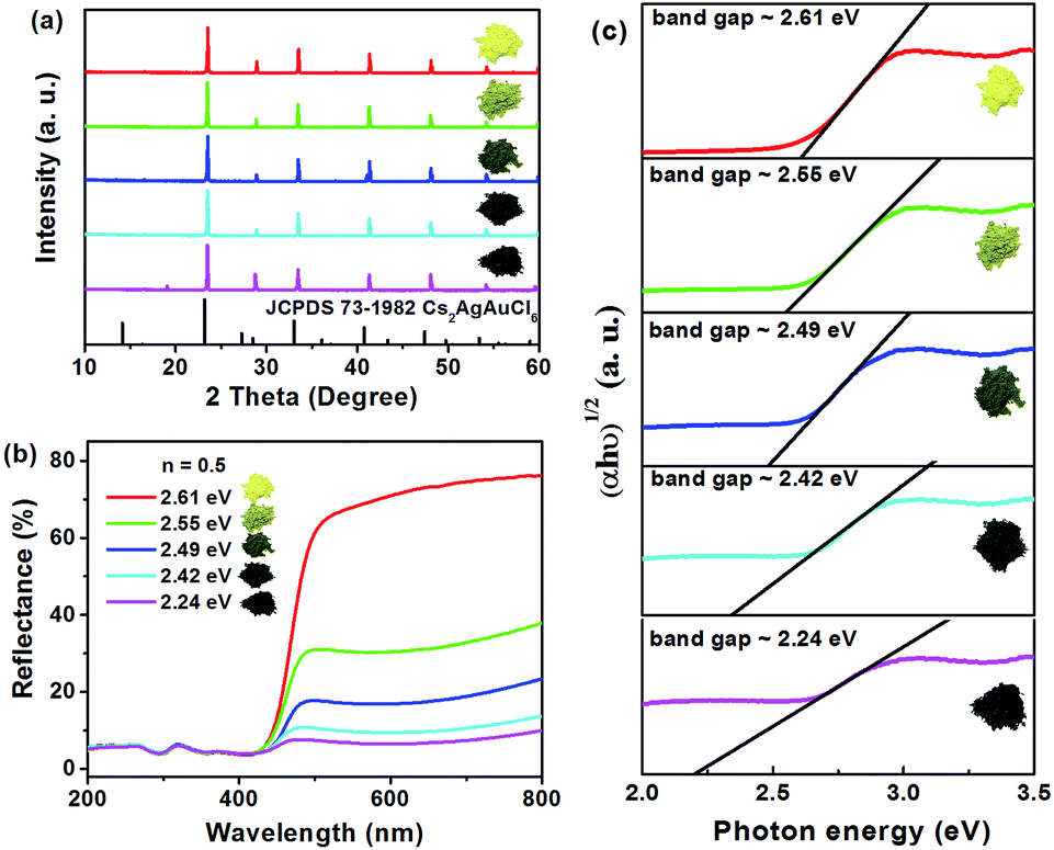
It is also worth mentioning that the body colors of the as-prepared powders can be continuously changed from yellow to dark green and eventually to near black with increasing volumes of HCl from 0.5 mL to 1.5 mL (Fig. 3a). Moreover, all of these samples are pure phase, and this phenomenon can be controlled by the added amount of HCl in the reaction solution. To determine the optical bandgaps for these different colored samples, the UV-vis diffuse reflection spectra of Cs2AgSbCl6 have been measured. As shown in Fig. 3b, as the color of the samples deepens, the reflection curve becomes lower and lower. The band gap of Cs2AgSbCl6 can be estimated according to eqn (1)30
| | | [F(R∞)hv]n = A(hv − Eg) | (1) |
where
hv is the photon energy;
A is a proportional constant;
Eg is the value of the band gap;
n = 2 for a direct transition or 1/2 for an indirect transition; and
F(
R∞) is the Kubelka–Munk function defined as
31| | | F(R∞) = (1 − R)2/2R = K/S | (2) |
where
R,
K, and
S are the reflection, absorption, and scattering coefficient, respectively. From the linear extrapolation of [
F(
R∞)
hv]
1/2 = 0 in
Fig. 3c, we can estimate an indirect optical band gap in the range of 2.61 eV to 2.24 ev with the color changing from yellow to near black.
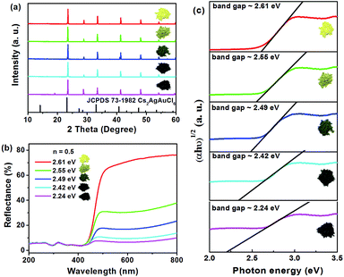 |
| | Fig. 3 Powder XRD patterns (a), UV-vis diffuse reflectance spectra (b), and Tauc plots (c) of different as-prepared Cs2AgSbCl6 obtained by using different amounts of HCl (0.5, 0.75, 1.0, 1.25 and 1.5 mL) with variable visible light absorbance. | |
3.2 Band structure and optical absorption calculations
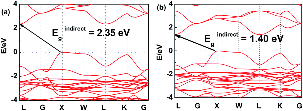
In order to further investigate this color-tuning phenomenon, we calculated the band structures using density functional theory (DFT). The details of the calculations are available in the Experimental section and the atomic structure used for the calculations is based on the X-ray diffraction data. Fig. 4 shows the electronic band structure of the double-perovskite Cs2AgSbCl6 by HSE (a) and PBE (b) calculations. Cs2AgSbCl6 showed an indirect band gap, with VBM at X (0.5, 0.5, 0) and CBM at L (0.5, 0.5, 0.5). The direct/indirect band gaps of primitive Cs2AgSbCl6 are 3.33/2.35 eV by HSE and 2.36/1.40 eV by PBE. As the electronic band structures obtained by these two approaches differ only in the band gaps, we choose the PBE approach to quantify the defect influence on the electronic and optical properties of Cs2AgSbCl6 in the following investigations.
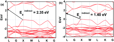 |
| | Fig. 4 Electronic band structure of the double-perovskite Cs2AgSbCl6 by HSE (a) and PBE (b) approaches. | |
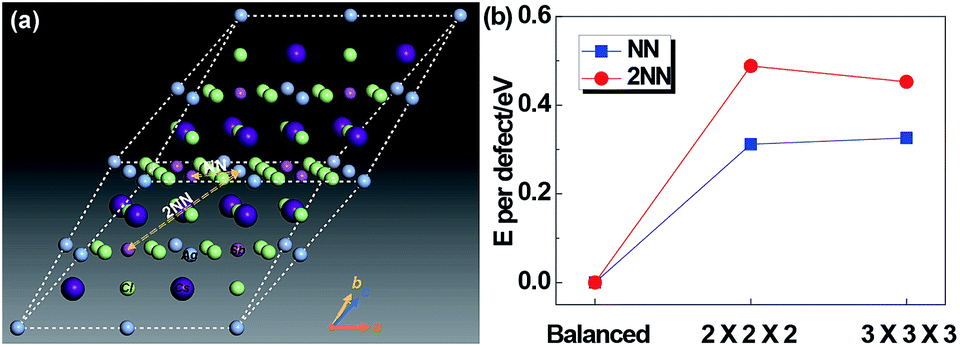
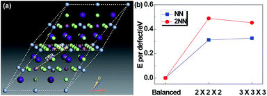
Since Ag and Sb have rather similar local environments in the present cubic double-perovskite Cs2AgSbCl6 phase (e.g. Ag[Cl6Cs8Sb6Ag12] and Sb[Cl6Cs8Ag6Sb12] that differ only in the third shell, and similar atomic radii (0.16 nm for Ag and 0.145 nm for Sb32)), it is worthwhile to study the anti-site defect between them. Furthermore, because we considered the anti-site defect with swapped Ag and Sb atoms, the ratio of each element will not be changed, making the defect structures possibly allomorphic. Fig. 5a shows a diagrammatic sketch of two anti-site defect models of Cs2AgSbCl6 structures based on a primitive (with a rhombic structure) enlarged 2 × 2 × 2 super cell (Cs16Ag8Sb8Cl48). In these two anti-site models, an Ag atom makes atomic transposition with its nearest neighbor (NN) Sb atom and second-nearest neighbor (2NN) Sb atom. Before selecting the size of the super cell, we tested the size effect of the defect energy, as shown in Fig. 5b. For NN and 2NN structures, Edefect has been converged in accordance with the results of 2 × 2 × 2 and 3 × 3 × 3 super cells, meaning that the 2 × 2 × 2 super cell is large enough to avoid the boundary effect caused by DFT calculations. And the structural parameters of primitive Cs2AgSbCl6 and 3 Cs16Ag8Sb8Cl48 (balanced, NN and 2NN) structures after full relaxation are shown in Table 3. Compared with the balanced structures, the lattices of NN and 2NN defect structures expanded and the total energy was increased by 0.625 eV (NN) and 0.975 eV (2NN) due to the influence of the internal defect on the lattice. For the NN anti-site model, the structure is no longer cubic, this is mainly because the transposition occurred within the diagonal of the face rather than the body diagonal, causing the lattice to expand uncoordinated with a distortion. For the 2NN anti-site model, the lattice also slightly expands (by 0.39%). Due to the relatively low formation energy of anti-site defects (e.g. 0.625 eV for the NN anti-site), a significant amount of Ag–Sb anti-site defects would form. The Ag and Sb anti-site defects would be connected to their NN, 2NN, 3NN,… neighboring anti-sites in the crystal.
 |
| | Fig. 5 (a) Diagrammatic sketch of the two anti-site defect models of Cs2AgSbCl6 structures. NN: transposition of Ag and its nearest neighbor Sb atom; 2NN: transposition of Ag and its second-nearest neighbor Sb atom. (b) Energy per defect for NN and 2NN structures for 2 × 2 × 2 and 3 × 3 × 3 Cs2AgSbCl6 super cells. | |
Table 3 Structural parameters of primitive Cs2AgSbCl6 and 3 Cs16Ag8Sb8Cl48 (balanced, NN and 2NN) structures
| Structure |
E
tot (eV) |
ΔE (eV) |
ΔE/atom (meV) |
V (Å3) |
L
a (Å) |
L
b (Å) |
L
c (Å) |
α (o) |
β (o) |
γ (o) |
| Primitive |
−32.703 |
— |
— |
319 |
7.672 |
7.672 |
7.672 |
60 |
60 |
60 |
| Balanced |
−261.625 |
0 |
0 |
2554 |
15.343 |
15.343 |
15.343 |
60 |
60 |
60 |
| NN |
−261.000 |
0.625 |
7.81 |
2586 |
15.397 |
15.424 |
15.397 |
59.94 |
60.12 |
59.94 |
| 2NN |
−260.650 |
0.975 |
12.19 |
2584 |
15.403 |
15.403 |
15.403 |
60 |
60 |
60 |
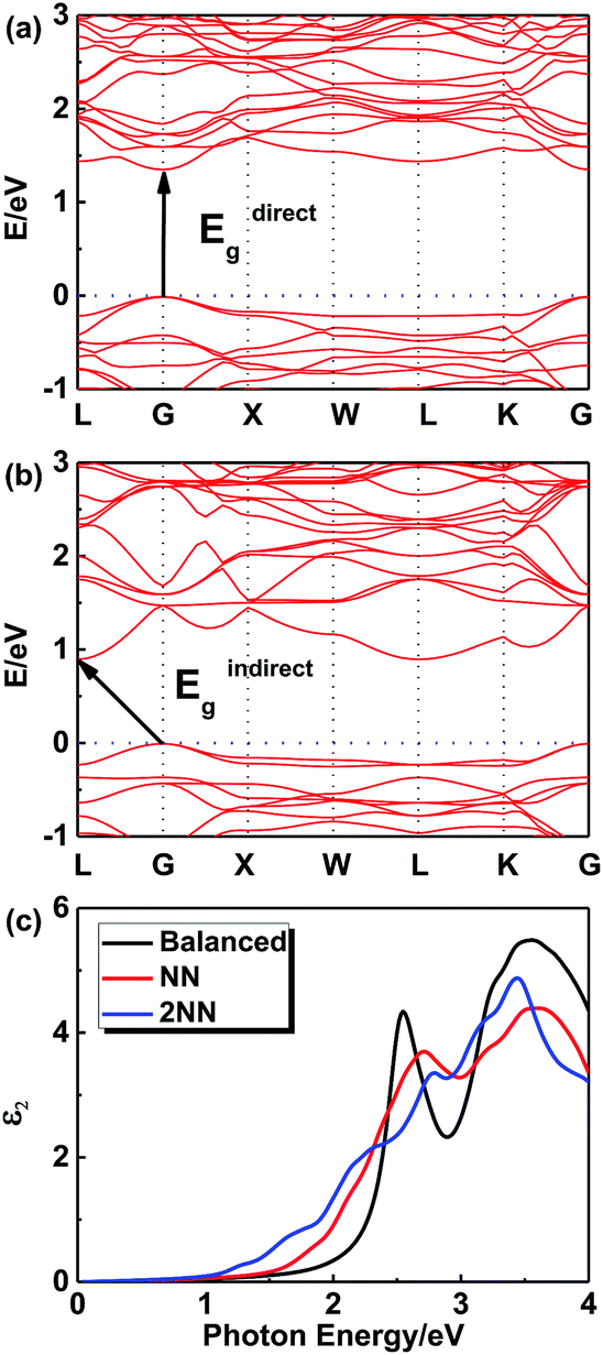
Fig. 6 shows the electronic band structures of NN (Fig. 6a) and 2NN (Fig. 6b) Cs16Ag8Sb8Cl48 anti-site structures from the PBE calculations, respectively. Since a super cell is required in the process of calculating defects, the band folding will occur and result in the gap fold of the band structure to the gamma point, so direct band gap is chosen to be discussed. The direct band gaps of the anti-site structures decrease from 2.36 eV (pristine) to 1.36 eV (NN) and 1.13 eV (2NN). The decrease of the direct gap from NN to 2NN anti-sites reflects the effect of the local electric field between the oppositely charged Ag and Sb anti-site defects. Details of band gaps are presented in Table 4. As NN and 2NN are allotropes of double-perovskite Cs2AgSbCl6 structures, the obvious gap differences indicate that this defect model could stand a good chance in the experiments.
 |
| | Fig. 6 Electronic band structure of NN (a) and 2NN (b) Cs16Ag8Sb8Cl48 anti-site structures from the PBE calculations. (c) Imaginary part of the dielectric functions of 3 Cs16Ag8Sb8Cl48 structures from the PBE calculations. | |
Table 4 Band gap of Cs2AgSbCl6 for different anti-site defect models and calculation methods
| Structure |
Calculation method |
E
directg/eV |
E
indirectg/eV |
E
overallg/eV |
| Primitive |
HSE |
3.33 |
2.35 |
2.35 |
| Primitive |
PBE |
2.36 |
1.40 |
1.40 |
| NN |
PBE |
1.36 |
— |
1.36 |
| 2NN |
PBE |
1.13 |
0.90 |
0.90 |
Fig. 6c shows the imaginary optical absorption coefficient of the dielectric functions of 3 Cs16Ag8Sb8Cl48 structures. The absorption edges coincided with the direct band gaps (see Table 4) and showed the order Ebalanced > ENN > E2NN, which is consistent with the band gap variation in these structures. As we discussed before, since a significant amount of anti-sites with NN, 2NN,… nearest neighbor configurations would form at the experimental temperature, Cs2AgSbCl6 would have strong optical absorption for photons with energy much lower than its pristine optical band gap. It would be hard to define strictly the actual optical gap of Cs2AgSbCl6 containing defects. However, the optical absorbance of Cs2AgSbCl6 containing defects towards visible light (below its optical band gap of ∼3.33 eV according to HSE calculations) can be continuously varied due to the formation of anti-site defects. Indeed, in the experiments, we observed almost continuously constant optical absorbance for most of the visible light in Cs2AgSbCl6 below its pristine optical band gap (see Fig. 3b) indicated by a clear optical absorption shoulder that doesn't change much for different samples (the variation of optical gap from 2.61 to 2.24 eV could not explain the significant variation of sample colors). The main difference between the samples with different colors is the magnitude of reflectance for visible light (see the right side of Fig. 3b), i.e. the darker sample absorbs more visible light, in other words it reflects less light. A possible reason is that the darker sample contains more Ag–Sb anti-site defects. Since 100% Ag–Sb anti-sites in Cs2AgSbCl6 lead to the same structure as the pristine crystal and zero defect formation energy, in local regions of Cs2AgSbCl6, clusters of Ag–Sb anti-sites could form, leading to high anti-site density. The formation of anti-site clusters is hard to control precisely in the current synthesis of bulk compounds. The above optical absorption feature is rather different from the widely studied tunability of sample color by controlling the sizes of nano-crystals (e.g. in ref. 33), where the optical absorption shoulder changes significantly for different samples with different nano-crystal sizes. In our experiments, we also observed a slight variation of optical absorption shoulders, which may reflect the change of nano-crystal sizes. Furthermore, although there are contributions from phonon assisted absorption in Fig. 3b, the phonon effect could not explain the sharp sample color variation since phonon assisted absorption could not go below the fundamental gap of pristine Cs2AgSbCl6 (2.35 eV according to HSE calculations). The variety of visible light absorbance in Cs2AgSbCl6 is related to the as-observed colors of the materials, which also have some implications for optical properties.
3.3 Chemical, light and thermal stability
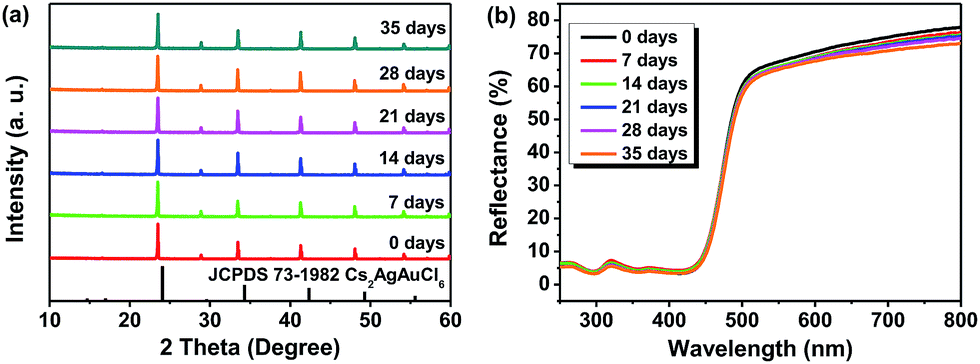
Regarding the environmental stability of Cs2AgSbCl6, the selected Cs2AgSbCl6 sample with Eg = 2.61 eV was exposed to the ambient atmosphere under both light and moisture conditions, with the powder XRD and UV-vis diffuse reflectance spectra monitored as a function of time (Fig. 7). It is found that there is nearly no apparent difference in the thermal and chemical stability depending on the crystal size. Hence, as can be seen in Fig. 7a, the powder XRD patterns for one month storage (in the ambient atmosphere) show no evidence of material decomposition, indicating that the material is rather stable. As for the reflectance spectrum, no obvious change was detected in the curve shape except for the slight intensity decline (Fig. 7b).
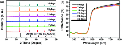 |
| | Fig. 7 PXRD patterns (a) and UV-vis diffuse reflectance spectra (b) of Cs2AgSbCl6 after 0 days, 7 days, 14 days, 21 days, 28 days and 35 days of exposure to light and moisture conditions. | |
Halide perovskites are known for low decomposition and formation energies. Since thermal stability is also an important parameter for halide perovskites in the prospective applications, we carried out thermogravimetric and differential scanning calorimetry (TG-DSC) analysis of a Cs2AgSbCl6 powder sample (Fig. 8). From the recorded TG-DSC result during the heat-treatment of Cs2AgSbCl6 in an argon flow, it is apparent that there are two major stages of rapid weight loss in the TGA curve at 356 and 756 °C, accompanying their corresponding exothermic peaks, which indicates that Cs2AgSbCl6 may decompose by two steps. The first weight loss of about 28.55 wt%, observed at 250–500 °C, is ascribed to the evaporation of SbCl3. Notably, SbCl3 constitutes 32.21% of the total weight of Cs2AgSbCl6, and therefore, the decomposition reaction equation might be described as follows: Cs2AgSbCl6 → SbCl3 + Cs2AgCl3. Finally, the third serious weight loss of 42.64 wt%, observed at 500–1000 °C and centered at around 756 °C, is in good agreement with the theoretical value of CsCl (47.55%) evaporation, and the decomposition process could proceed according to the scheme below: Cs2AgCl3 → AgCl + 2CsCl.34 The above results showed that Cs2AgSbCl6 is relatively stable to mass loss up to 250 °C. After that, some obvious decomposition reaction occurs enabling the materials to lose the functionality completely.
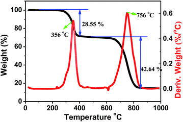 |
| | Fig. 8 TGA and DSC data for a powder sample of Cs2AgSbCl6. | |
4 Conclusion
In summary, we have designed and prepared phase pure crystals of Cs2AgSbCl6via hydrothermal routes, which is relatively stable and non-toxic and has a low band gap. To demonstrate the transposition influence on the electronic and optical properties of Cs2AgSbCl6, focusing a combined experimental and theoretical study, we established an anti-site defect model by density functional theory (DFT). By exchanging site-equal Ag and Sb ions, the two allotropes (NN and 2NN) are thermodynamically stable with only 7–12 meV per atom larger than the balanced structure, and the band gap could be varied with relatively small lattice expansion. Overall, the discovery of Cs2AgSbCl6 furthermore stresses the importance of the double perovskite approach in the search for lead-free photovoltaic materials that exhibit good stability.
Conflicts of interest
There are no conflicts to declare.
Acknowledgements
The present work was supported by the National Natural Science Foundation of China (Grants 91622125, 51572023, 11774239 and 51722202), Natural Science Foundations of Beijing (2172036), and National Key R&D Program of China (Grant 2016YFB0700700). M. Molokeev acknowledges the support of the Russian Foundation for Basic Research (17-52-53031).
Notes and references
- J. Seo, J. H. Noh and S. I. Seok, Acc. Chem. Res., 2016, 49, 562–572 CrossRef CAS PubMed.
- A. Kojima, K. Teshima, Y. Shirai and T. Miyasaka, J. Am. Chem. Soc., 2009, 131, 6050–6051 CrossRef CAS PubMed.
- N. J. Jeon, J. H. Noh, Y. C. Kim, W. S. Yang, S. Ryu and S. I. Seok, Nat. Mater., 2014, 13, 897–903 CrossRef CAS PubMed.
- S. D. Stranks, G. E. Eperon, G. Grancini, C. Menelaou, M. J. Alcocer, T. Leijtens, L. M. Herz, A. Petrozza and H. J. Snaith, Science, 2013, 342, 341–344 CrossRef CAS PubMed.
- T. Yokoyama, D. H. Cao, C. C. Stoumpos, T. B. Song, Y. Sato, S. Aramaki and M. G. Kanatzidis, J. Phys. Chem. Lett., 2016, 7, 776–782 CrossRef CAS PubMed.
- G. Volonakis, M. R. Filip, A. A. Haghighirad, N. Sakai, B. Wenger, H. J. Snaith and F. Giustino, J. Phys. Chem. Lett., 2016, 7, 1254–1259 CrossRef CAS PubMed.
- F. Giustino and H. J. Snaith, ACS Energy Lett., 2016, 1, 1233–1240 CrossRef CAS.
- C. C. Stoumpos, L. Frazer, D. J. Clark, Y. S. Kim, S. H. Rhim, A. J. Freeman, J. B. Ketterson, J. I. Jang and M. G. Kanatzidis, J. Am. Chem. Soc., 2015, 137, 6804–6819 CrossRef CAS PubMed.
- F. Hao, C. C. Stoumpos, D. H. Cao, R. P. H. Chang and M. G. Kanatzidis, Nat. Photonics, 2014, 8, 489–494 CrossRef CAS.
- Z. W. Xiao, W. W. Meng, J. B. Wang, D. B. Mitzi and Y. F. Yan, Mater. Horiz., 2017, 4, 206–216 RSC.
- S. J. Sun, S. S. Tominaka, J. H. Lee, F. Xie, P. D. Bristowe and A. K. Cheetham, APL Mater., 2016, 4, 31101 CrossRef.
- P. F. Cheng, T. Wu, Y. J. Li, L. Jiang, W. Q. Deng and K. L. Han, New J. Chem., 2017, 41, 9598–9601 RSC.
- X. G. Zhao, J. H. Yang, Y. Fu, D. Yang, Q. Xu, L. Yu, S. H. Wei and L. Zhang, J. Am. Chem. Soc., 2017, 139, 2630–2638 CrossRef CAS PubMed.
- E. T. McClure, M. R. Ball, W. Windl and P. M. Woodward, Chem. Mater., 2016, 28, 1348–1354 CrossRef CAS.
- S. Vasala and M. Karppinen, Prog. Solid State Chem., 2015, 43, 1–36 CrossRef CAS.
- L. R. Morss, M. Siegal, L. Stenger and N. Edelstein, Inorg. Chem., 1970, 9, 1771–1775 CrossRef CAS.
- J. Zhou, Z. G. Xia, M. S. Molokeev, X. W. Zhang, D. S. Peng and Q. L. Liu, J. Mater. Chem. A, 2017, 5, 15031–15037 CAS.
- T. T. Tran, J. R. Panella, J. R. Chamorro, J. R. Morey and T. M. McQueen, Mater. Horiz., 2017, 4, 688–693 RSC.
-
Bruker AXS, TOPAS V4: General Profile and Structure Analysis Software for Powder Diffraction Data-User's Manual, Bruker AXS, Karlsruhe, Germany, 2008 Search PubMed.
- G. Kresse and J. Hafner, Phys. Rev. B: Condens. Matter Mater. Phys., 1993, 47, 558–561 CrossRef CAS.
- G. Kresse and J. Furthmüller, Phys. Rev. B: Condens. Matter Mater. Phys., 1996, 54, 11169 CrossRef CAS.
- P. E. Blöchl, Phys. Rev. B: Condens. Matter Mater. Phys., 1994, 50, 17953–17979 CrossRef.
- J. P. Perdew, K. Burke and M. Ernzerhof, Phys. Rev. Lett., 1996, 77, 3865 CrossRef CAS PubMed.
- H. J. Monkhorst and J. D. Pack, Phys. Rev. B: Solid State, 1976, 13, 5188–5192 CrossRef.
- A. V. Krukau, O. A. Vydrov, A. F. Izmaylov and G. E. Scuseria, J. Chem. Phys., 2006, 125, 224106 CrossRef PubMed.
- N. Elliott and L. Pauling, J. Am. Chem. Soc., 1938, 60, 1846–1851 CrossRef CAS.
- V. V. Atuchin, A. S. Aleksandrovsky, O. D. Chimitova, T. A. Gavrilova, A. S. Krylov, M. S. Molokeev, A. S. Oreshonkov, B. G. Bazarov and J. G. Bazarova, J. Phys. Chem. C, 2014, 118, 15404–15411 CAS.
- V. V. Atuchin, N. F. Beisel, E. N. Galashov, E. M. Mandrik, M. S. Molokeev, A. P. Yelisseyev, A. A. Yusuf and Z. Xia, ACS Appl. Mater. Interfaces, 2015, 7, 26235–26243 CAS.
- V. V. Atuchin, A. S. Aleksandrovsky, M. S. Molokeev, A. S. Krylov, A. S. Oreshonkov and D. Zhou, J. Alloys Compd., 2017, 729, 843–849 CrossRef CAS.
- J. Zhou, Z. G. Xia, M. Bettinelli and Q. L. Liu, RSC Adv., 2016, 6, 2046–2054 RSC.
- Z. G. Xia, Y. Y. Zhang, M. S. Molokeev and V. V. Atuchin, J. Phys. Chem. C, 2013, 117, 20847–20854 CAS.
- J. C. Slater, J. Chem. Phys., 1964, 41, 3199–3204 CrossRef CAS.
- V. Malgras, S. Tominaka, J. W. Ryan, J. Henzie, T. Takei, K. Ohara and Y. Yamauchi, J. Am. Chem. Soc., 2016, 138, 13874–13881 CrossRef CAS PubMed.
- F. P. Emmenegger, J. Cryst. Growth, 1972, 17, 31–37 CrossRef CAS.
Footnotes |
| † Electronic supplementary information (ESI) available: The crystallographic information (CIF) of Cs2AgSbCl6. See DOI: 10.1039/c7ta10062k |
| ‡ These authors contributed equally. |
|
| This journal is © The Royal Society of Chemistry 2018 |
Click here to see how this site uses Cookies. View our privacy policy here. 
 Open Access Article
 This Open Access Article is licensed under a
  def,
Xiuwen
Zhang
*b and
Zhiguo
Xia
def,
Xiuwen
Zhang
*b and
Zhiguo
Xia