
Benzothiadiazole–triphenylamine as an efficient exciton blocking layer in small molecule based organic solar cells†
Laura
Caliò
a,
Bhushan R.
Patil
 d,
Johannes
Benduhn
e,
Koen
Vandewal‡
e,
Horst-Günter
Rubahn
d,
Morten
Madsen
d,
Samrana
Kazim
*ab and
Shahzada
Ahmad
*abc
d,
Johannes
Benduhn
e,
Koen
Vandewal‡
e,
Horst-Günter
Rubahn
d,
Morten
Madsen
d,
Samrana
Kazim
*ab and
Shahzada
Ahmad
*abc
aAbengoa Research, Abengoa, C/Energía Solar no. 1, Campus Palmas Altas-41014, Sevilla, Spain
bBCMaterials, Basque Center for Materials, Applications and Nanostructures, UPV/EHU Science Park, 48940 Leioa, Spain. E-mail: samrana.kazim@bcmaterials.net; shahzada.ahmad@bcmaterials.net; Tel: +34 946128811
cIKERBASQUE, Basque Foundation for Science, Bilbao, 48013, Spain
dSDU NanoSYD, Mads Clausen Institute, University of Southern Denmark, Alsion 2, 6400 Sønderborg, Denmark
eDresden Integrated Center for Applied Physics and Photonic Materials (IAPP), Institute for Applied Physics, Technische Universität Dresden, Nöthnitzer Str. 61, 01187 Dresden, Germany
First published on 3rd August 2018
Abstract
We have designed a small molecule based on benzothiadiazole–triphenylamine moieties (BTD–TPA2), composed of an electron-poor benzothiadiazole core with two electron-rich triphenylamine arms. BTD–TPA2 was synthesized in a facile manner using a Suzuki cross-coupling reaction. The molecule was rationally designed to take advantage of the synergistic effect of BTD, which allows the formation of a favorable band gap material, and triphenylamine (TPA) moieties, which favour efficient hole extraction and transport properties. A thin layer of BTD–TPA2 was placed between the photo-active DBP/C70 layer stack and the MoOx electrical contact. With an optimized interlayer thickness of 35 nm, the attained photovoltaic properties were substantially superior to those of the reference devices. This has its origin in the dual functionality of BTD–TPA2, i.e., efficient exciton blocking and improved hole extraction at the anode contact. The obtained results led to an improved power conversion efficiency of 5.66% for a vacuum deposited bilayer DBP/C70 solar cell, which will be the new state of the art for bilayer DBP based solar cells.
Introduction
Organic solar cells (OSCs) have been intensively investigated over the last few decades with the aim of further optimizing their photovoltaic (PV) performance, currently exhibiting power conversion efficiency (PCE) values of up to 15%.1 OSCs have a competitive edge due to their intriguing features such as low cost of material and fabrication,2,3 and the possibility of using roll-to-roll (R2R) processing techniques,4,5 along with the possibility of developing thin, aesthetic, flexible, transparent and portable solar modules6–9 as compared to other thin film PV technologies. Diverse device architectures have been investigated so far, such as donor and acceptor (D–A) bilayer (planar heterojunction, PHJ) and bulk heterojunction (BHJ) structures, in conjunction with innovative materials, such as polymeric semiconductors and small organic molecules as donor and acceptor materials. Small organic molecules possess numerous benefits, such as high purity, easy processability and low batch-to-batch variation in performance, which allows the exploration of a range of novel materials for use as donor and acceptor molecules in OSCs.10,11 Tetraphenyldibenzoperiflanthene (DBP) as the donor and C70 as the acceptor material have been well investigated and employed in both efficient bulk12 and bilayer13,14 heterojunction OSC configurations. DBP is a well-known small organic conjugated material, and has been extensively used in opto-electrical devices, and OSCs in particular.15–17 The main advantages of using DBP as a donor material in OSCs are its high optical absorption and relatively deep lying highest occupied molecular orbital (HOMO) level (−5.5 eV (ref. 18)), which was found to be ideal for efficient exciton splitting at the DBP/fullerene interface, while maintaining relatively high open circuit voltages (VOC).13,19 DBP has a strong absorption in the visible region from 300 to 700 nm, with a peak absorption coefficient of 4.2 × 105 cm−1 at λ = 610 nm, a relatively high hole mobility of ∼10−4 cm2 V−1 s−1,19 and an exciton diffusion length of up to 16 ± 1 nm, as reported by Bergemann et al.20 DBP based devices employing MoOx as hole extraction layers were found to yield decent performance, though excitons were not blocked at the DBP/MoOx interface, but were quenched.21 A possible strategy for overcoming exciton quenching effects is to introduce an exciton blocking layer (EBL), which can prevent excitons from leaving the active layer, and increases the possibility for dissociation at the D–A interface.19 Zhang et al. have reported the use of three well-known small organic hole transporting materials (HTMs), 5,10,15-tribenzyl-5H-diindolo[3,2-a:3′,2′-c]-carbazole (TBDI), N,N′-diphenyl-N,N′-bis(1-naphthyl)-1,1′-biphenyl-4,4′-diamine (NPB) and 1,1′-bis(di-4-tolylaminophenyl)cyclohexane (TAPC), to serve as an EBL in DBP based planar heterojunction cells.22 It was reported that the HTM successfully blocked excitons at the donor/hole extraction interface, yielding a PCE of 1.70%, 1.33%, and 1.33%, respectively, whereas the control device without any EBL gave a modest PCE of 1.25%. Patil et al.14 have recently reported an analogous study in which an ultra-thin layer of N,N′-di-1-naphthalenyl-N,N′-diphenyl[1,1′:4′,1′′:4′′,1′′′-quaterphenyl]-4,4′′′-diamine (4P-NPD) was effectively used as an EBL in DBP/C70 inverted planar heterojunction solar cells, yielding a PCE of 3.69% for the optimized EBL thickness versus a PCE of 2.97% for the EBL-free reference cell. In this work, we have introduced 4,4′-(2,1,3-benzothiadiazole-4,7-diyl)bis(N,N-diphenylaniline) (BTD–TPA2) as an EBL, sandwiched between the electron donor (DBP) and the hole transporting layer (MoOx) in a classical planar heterojunction solar cell. The use of BTD–TPA2 demonstrates its dual functionality, i.e., efficient exciton blocking and improved hole extraction at the anode as well as electron co-donor effect. The obtained results led to an improvement in the device performance in terms of PCE, and an enhanced PCE of 5.66% for bilayer DBP/C70 solar cells was obtained with an optimized EBL thickness of 35 nm (15 mM BTD–TPA2), which is among the highest reported PCEs to date for bilayer DBP based solar cells.Results and discussion
Fig. 1 presents the architecture of the devices studied in this work along with the molecular structure of the materials used. MoOx was employed as a hole transporting layer in the OSCs, due to its efficient and stable hole extraction capabilities.23,24 A thin layer of 2,9-dimethyl-4,7-diphenyl-1,10-phenathroline (bathocuproine, BCP) was used as an electron transporting material and hole blocking layer at the interface between the C70 acceptor and the Ag cathode. BCP is a wide band gap electron transporting material, which also acts as a physical barrier in order to prevent damage to the active organic layer due to the metal deposition. In a report, the Ag metal:BCP hybrid complex formed upon Ag evaporation was found to possess favorable states (LUMO level of the complex) inside the bandgap of BCP, leading to an efficient electron extraction in such OSCs.25 In the past, benzothiadiazole (BTD) based polymers and small molecules have been widely employed in opto-electrical devices, such as organic light emitting diodes (OLEDs), due to their fluorescence properties,26,27 while D–A structures in combination with triphenylamine (TPA) moieties have been extensively employed as dye/active materials in dye sensitized solar cells (DSSCs)28,29/OSCs.30,31 BTD–TPA2 is a small organic molecule having an electron-poor benzothiadiazole core with two electron-rich triphenylamine arms, and has been explored as a red light-emitting material for application in OLEDs.32,33 | ||
| Fig. 1 (a) Band alignment and (b) molecular structure of the materials used in this study. | ||
BTD–TPA2 was synthesized in a facile manner using a Suzuki cross-coupling reaction (Scheme 1). The 1H-NMR spectrum of the synthesized BTD–TPA2 was recorded in CD2Cl2 and is shown in Fig. S1 (ESI†). The presence of triphenylamine (TPA) moieties provides an amorphous thin film with efficient hole transport properties, while the presence of the BTD core leads to a suitable frontier orbital energy matching with the donor of the HOMO.34 Differential scanning calorimetry (DSC) results, thermogravimetric analysis (TGA) curves and cyclic voltammetry (CV) measurements are reported in Fig. S2 (ESI†), showing a HOMO level of −5.54 eV and a LUMO level of −3.24 eV, which is higher than the LUMO level of DBP, allowing the use of BTD–TPA2 as an exciton blocking material and potential donor in such devices (the chemical structure and band alignment are shown in Fig. 1).
 | ||
| Scheme 1 Synthetic route adopted for the synthesis of BTD–TPA2. | ||
To optimize the thickness of the films, various concentrations (eight different samples) of BTD–TPA2 were prepared in chlorobenzene, and were spin-coated (under similar conditions) to form an interfacial layer between the thermally evaporated layers of MoOx and DBP (structure depicted in Fig. 1). The concentrations of BTD–TPA2 were chosen in such a way so as to allow for the formation of a thin layer and were in the range of 1.25–40 mM (the corresponding thickness was in between 15 to 65 nm). To elucidate the effect of BTD–TPA2, reference devices (without an EBL, labelled as 0 mM) were also fabricated. The fabricated devices have the following structure: ITO/MoOx (10 nm)/BTD–TPA2 (0–65 nm)/DBP (20 nm)/C70 (30 nm)/BCP (10 nm)/Ag (100 nm).
The employment of BTD–TPA2 as an EBL gave notable enhancements in the PV performance of the devices, as shown in Table 1, while statistical values are reported in Table S1 (ESI†).
| Concentration/thickness of BTD–TPA2 | V OC (mV) | J SC (mA cm−2) | FF (%) | PCE (%) |
|---|---|---|---|---|
| 40 mM/65 nm | 870 | 6.81 | 39.00 | 2.32 |
| 30 mM/45 nm | 940 | 7.86 | 46.71 | 3.14 |
| 20 mM/40 nm | 940 | 8.84 | 54.56 | 4.56 |
| 15 mM/35 nm | 950 | 9.53 | 62.73 | 5.66 |
| 10 mM/30 nm | 940 | 9.66 | 56.38 | 5.13 |
| 5 mM/25 nm | 950 | 7.69 | 63.42 | 4.62 |
| 2.5 mM/20 nm | 950 | 7.34 | 61.88 | 4.31 |
| 1.25 mM/15 nm | 860 | 6.56 | 68.92 | 3.88 |
| 0 mM/0 nm | 900 | 6.69 | 64.86 | 3.91 |
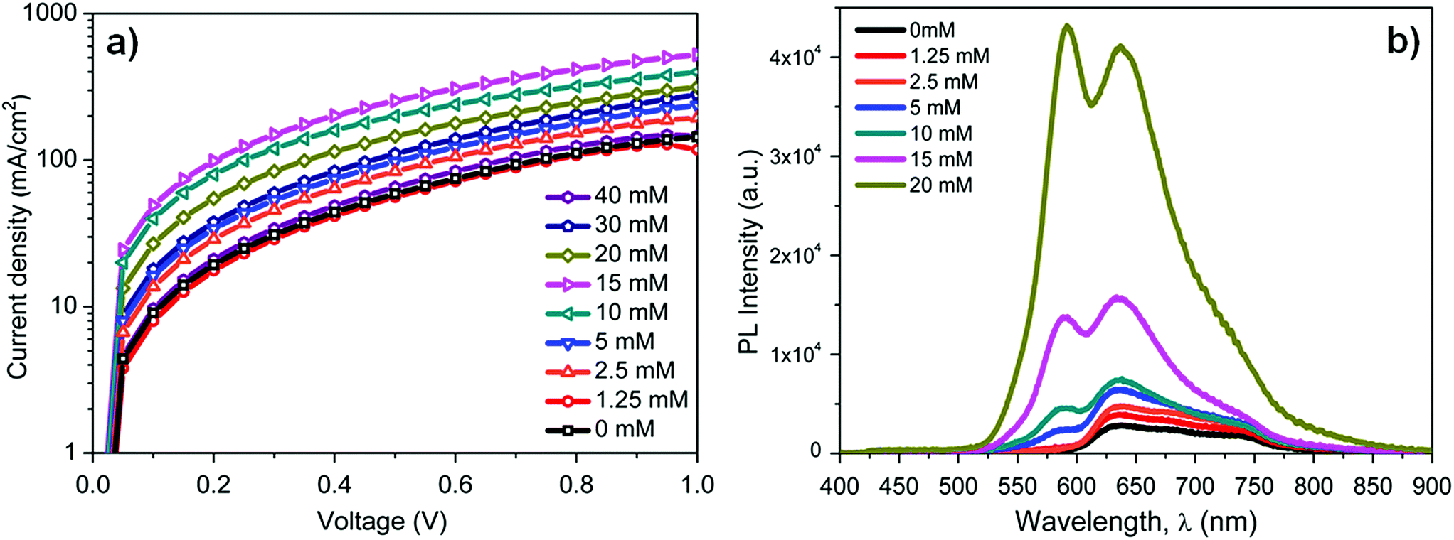
Enhancements in the short-circuit current density (JSC) were obtained for all the devices fabricated by using BTD–TPA2 as an EBL. For the optimal thickness of BTD–TPA2 (15 mM with a corresponding thickness of 35 nm), the current density value obtained was nearly 42% higher than the JSC of the reference devices, i.e., an increment was observed from 6.7 mA cm−2 for the EBL-free reference devices to 9.5 mA cm−2 for the best device containing BTD–TPA2. Thus, the enhancement in the photocurrent indicates the efficacy of the exciton-blocking properties of BTD–TPA2. The trends for the different BTD–TPA2 concentrations are distinct (Fig. 2 and 3a). The PV behaviour obtained from the thinnest EBL (1.25 mM solution, corresponding to a 15 nm thick layer) shows no significant improvement, yielding an VOC of 860 mV, a JSC of 6.56 mA cm−2, and a Fill Factor (FF) of 68.92% with an overall PCE of 3.88%, which are on a par with the reference devices (PCE = 3.91%). By increasing the concentration and thus thickness, i.e. to 2.5 mM and 5 mM (20 and 25 nm thick layers, respectively), a modest increase of the current density was registered due to the exciton blocking behavior of BTD–TPA2, from a JSC of 6.69 mA cm−2 for the reference device to 7.34 mA cm−2 and 7.69 mA cm−2 for the devices prepared with BTD–TPA2 at 2.5 mM and 5 mM, respectively. The significant improvements that were achieved with the devices containing the EBL deposited from the solution at 15 mM concentration gave an impressive overall PCE of 5.66%, which corresponds to an enhancement of over 42% with respect to the reference device. Notably, by further increasing the concentration to 20, 30 and 40 mM (i.e. 40, 45 and 65 nm thick layers), a reverse trend was obtained, and lower device performance was recorded, i.e. PCE of 4.56%, 3.14% and 2.32%, respectively. VOC remained largely constant, though an increase of 40–50 mV for devices containing the BTD–TPA2 layers (between 2.5 mM and 30 mM) was recorded. A drop in FF was obtained, in the case of thicker layers, deposited from solutions at 30 and 40 mM concentrations. This we attributed to an enhancement in series resistance caused by hampering of hole transport through the thicker EBL layer. These trends are also in accordance with the EQE measurements (Fig. 3b). The maximum light harvesting ability was attributed to the defined optimal concentration of BTD–TPA2, i.e. 15 mM, showing a maximum conversion of over 60% in the 550–650 nm range, which corresponds to the peak of DBP absorption, whereas an almost constant increment in the EQE spectrum was observed in the range of 300–650 nm. We expect that a co-donor effect may take place, allowing excitons generated in the BTD–TPA2 layer (absorbing at shorter wavelengths as compared to DBP in the range of 400–550 nm) to dissociate into free carriers. From the measured EQE curves, the integrated value of JSC was extracted for each configuration (Fig. S3†) and the values are listed in Table S1.† The integrated current density was consistent with the average values of current density obtained by the J–V measurements (Table S1†).
 | ||
| Fig. 2 Summary of the photovoltaic parameters obtained as a function of BTD–TPA2 concentration. | ||
 | ||
| Fig. 3 (a) J–V characteristics and (b) EQE measurements of OSCs fabricated with the BTD–TPA2 exciton blocking layer deposited from solutions at different concentrations. | ||
To further confirm whether a co-donor effect takes place, we calculated the change in EQE as a function of wavelength and its corresponding integrated photocurrent contributed by BTD–TPA2 as a co-donor (Fig. S4 and S5†). It can be deduced from the figure that in the case of a thin layer (1.25 mM, corresponding to a 15 nm thin film) and for a thicker layer (40 mM, corresponding to 65 nm thickness), there is a decreases in ΔEQE; thus, we don't expect any contribution from photons. However, an increase in ΔEQE can be observed from 2.5 mM to 15 mM (corresponding to thin layers of 20–35 nm thickness), which we assign to the co-donor effect of BTD–TPA2. Beyond this concentration, for 20 and 30 mM concentrations (corresponding to 40 and 45 nm thick layers), no enhancement in ΔEQE was observed and the contribution decreased. It can be concluded that a co-donor effect occurs when thin EBL layers (20–35 nm) are employed, and this effect is inefficient in the case of thick layers (40–65 nm). We expect that for thin layers, the excitons generated in the blocking layer are capable of reaching and dissociating at the DBP interface and this dissociation efficiency could be expected to drop for thicker layers (very thick layers of 40–65 nm), where instead the blocking improves further (as seen from PL results).
The thickness of the EBLs at different concentrations was measured with the help of atomic force microscopy (AFM) as shown in Fig. S7.† The average values from the measurement of each film deposited atop 10 nm of thermally evaporated MoOx are listed in Table S2.† The measured thickness was in the range of 15 nm (1.25 mM)–65 nm (40 mM). The best PV behavior was obtained from the deposition of 30–35 nm BTD–TPA2 as the EBL, corresponding to a concentration of 10–15 mM.
Fig. 4a shows the UV-vis absorption spectra of BTD–TPA2 layers deposited from the different concentration solutions sandwiched between the thermally evaporated MoOx and DBP layers. As expected, with the increase of concentration (and thus the thickness of BTD–TPA2 layers), the absorption in the range of 400–500 nm and 300–350 nm sequentially increases, which corresponds to the absorption of the synthesized molecules, as shown in Fig. 4a (black dotted line). Additionally, with the increase in the thickness of the EBL, a small reduction in the absorption of the peak at 610 nm was observed. As BTD–TPA2 lacks absorbance in this range, we expect that this relatively small absorption change could occur due to changes in the orientation of the DBP molecules when deposited on top of BTD–TPA2, as compared to on top of the MoOx layer.
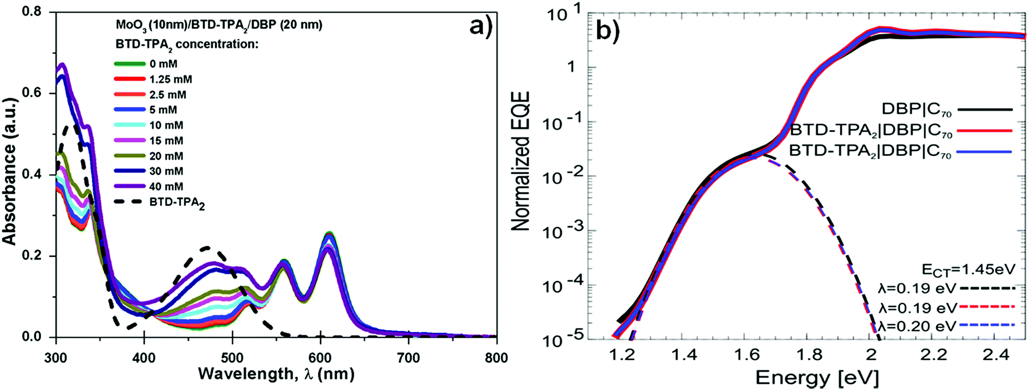 | ||
| Fig. 4 (a) UV-vis absorption spectra of the BTD–TPA2 layers sandwiched between MoOx and DBP layers (solid lines) and BTD–TPA2 alone (dashed line) and (b) sensitive-EQE measurements of the DBP/C70-based reference device (black line) and two devices with BTD–TPA2 using the best concentration (15 mM, red and blue lines). | ||
Due to the relatively strong absorption of BTD–TPA2 in the 400–550 nm range, which is complementary to the DBP main absorption at 550–650 nm, its usage as a single donor and as a co-donor with DBP was evaluated. For this purpose, two different thicknesses were selected to be evaluated as a donor layer, 40 nm and 35 nm, which correspond to 20 mM and 15 mM solutions, respectively, and were deposited by spin-coating under similar conditions. Similarly, in order to evaluate its behavior as a DBP co-donor, the concentrations of BTD–TPA2 (15 and 20 mM) were kept the same and they were probed together with an ultra-thin layer of DBP (5 nm). On the one hand, it can be deduced from data (Fig. S7 and Table S3 in ESI†) that the donor properties of BTD–TPA2 are less appealing compared to those of the reference donor DBP, resulting in devices with a maximum PCE of 2.44% for BTD–TPA2 with 40 nm thickness, while a PCE of 3.91% was obtained for the reference DBP device. On the other hand, the use of BTD–TPA2 as a co-donor with an ultrathin layer of DBP showed a slight improvement in device PCE, especially for the devices with the higher concentration of BTD–TPA2, i.e. 20 mM, resulting in a JSC of up to 8.01 mA cm−2 and a PCE of up to 4.19%. No significant change in terms of VOC was observed. These results suggest that the use of BTD–TPA2 as a donor with DBP is a less useful strategy as compared to its exciton blocking properties. However, when used as an exciton blocking layer, the co-donor effect will also be present, depending on the thickness of the EBL layer (Fig. S7†). Slight variations in the DBP absorption and open-circuit voltage were detected, which point towards a possible structurally modified donor layer. Thus, sensitive external quantum efficiency measurements (sEQE) were conducted to elucidate if the integrated BTD–TPA2 layer affects the interface energetics and the properties of the charge-transfer (CT) states at the donor/acceptor interface in the solar cells. In Fig. 4b, sEQE measurements of the DBP/C70-based reference device (black line) and for the configuration containing BTD–TPA2 at the best concentration (15 mM, red and blue lines) are shown. The two devices with the same concentration of BTD–TPA2 show an identical behavior. The signal at low photon energy of around 1.5 eV originates from the weak absorption related to the CT state between the C70 and DBP layers. From the sEQE measurements, the energy (ECT) and reorganization energy (λ) of the CT state were determined by fitting the low energy part of the spectrum as described by Vandewal et al.35 These parameters mainly determine the VOC.36,37 Since no difference for both ECT and λ in the reference DBP/C70 device and the BTD–TPA2/DBP/C70-based devices was found, we conclude that the interface energetics of DBP/C70 remain unchanged with the use of BTD–TPA2, suggesting that the main function of the layer is to provide efficient hole extraction and exciton blocking at the anode, in addition to the small co-donor effect. Additionally, it suggests that non-radiative voltage losses are reduced due to reduced non-radiative recombination at the hole contact, resulting in an increase in VOC.
To elucidate the effects of the implemented layers on the hole extraction properties, J–V measurements of hole only devices with different thicknesses of the BTD–TPA2 layers were conducted. The results from the hole only devices are shown in Fig. 5a. In the developed configuration, holes were injected into the device through the Ag electrode and extracted out of the device at the ITO electrode. Devices with the thickest BTD–TPA2 layer (40 mM) show the lowest extraction properties, corresponding to a lower current density, and are on a par with the EBL-free devices. Devices with BTD–TPA2 layers deposited from solutions at 10–15 mM concentrations presented the highest hole extraction efficiencies, demonstrating that the hole contact improves with the introduction of the BTD–TPA2 layer (up to 15 mM), but it decreases again due to the increased series resistance arising from the use of thicker layers (obtained using BTD–TPA2 above 15 mM).
 | ||
| Fig. 5 (a) J–V characteristics of the hole only devices (HODs), fabricated with the architecture ITO/MoOx (10 nm)/BTD–TPA2 (different thicknesses)/DBP (20 nm)/Ag (100 nm). (b) Photoluminescence measurements of the layer stack: quartz/MoOx (10 nm)/BTD–TPA2/DBP (15 nm). | ||
To illustrate the exciton blocking properties of BTD–TPA2, photoluminescence (PL) measurements were performed to compare the PL intensity of DBP using different concentrations of BTD–TPA2. The excitation wavelength was centred between 330 nm and 380 nm. Fig. 5b depicts the PL measurements of the layer stack: quartz/MoOx (10 nm)/BTD–TPA2/DBP (15 nm). The PL intensity of DBP (600–800 nm) with an emission maximum at 635 nm increases linearly up to a certain concentration (10 mM, corresponding to 30 nm thickness), and beyond the 10 mM BTD–TPA2 concentration, the PL signal increases rapidly up to 20 mM (40 nm thick EBL). At higher concentrations of 30 mM and 40 mM (corresponding to thicknesses of 45 and 65 nm, respectively), the PL intensity reaches the spectrometer detection limit, as shown in Fig. S8.†
With an increase in the thickness of the BTD–TPA2 layer, exciton quenching at the MoOx interface decreased, which led to an increased PL intensity. This directly demonstrates its effective exciton blocking capabilities by inhibiting charge recombination at the DBP donor and MoOx interface. We noted that in addition to the DBP signal, a PL signal from the BTD–TPA2 layers (centered at 585 nm) arises at a concentration of 5 mM (25 nm thickness). This PL signal further increases on increasing the BTD–TPA2 layer thickness, and surpasses the intensity of the DBP main peak for concentrations above 15 mM. The enhancement in PL emission at 585 nm also indicates that BTD–TPA2 participates simultaneously in the light absorption and exciton generation in the BTD–TPA2 layer and suggests its co-donor effect.
Conclusions
We put forward small organic molecules based on BTD–TPA2 moieties, which was synthesized using a simple Suzuki cross-coupling reaction and was employed as an effective exciton blocking material. The incorporation of BTD–TPA2 significantly improves the photovoltaic performance of DBP/C70 based solar cells. By tuning the concentration of BTD–TPA2, we found that the optimal BTD–TPA2 thickness for device integration is around 30–35 nm. Significant improvements in the short-circuit current density were achieved, with an astonishing increment of up to 45%, as compared to the JSC of the reference devices. This allowed us to achieve a notable increase in PCE from 3.91% to 5.66%, which is one of the highest efficiencies obtained to date in DBP based bilayer solar cells. In order to elucidate the mechanisms involved, PL measurements were performed to confirm the exciton blocking properties of BTD–TPA2, while hole-only devices revealed improved hole contact at low BTD–TPA2 thicknesses, with an optimal performance for the 30–35 nm thick layer. Additionally, sEQE measurements revealed no difference in the interface energetics at the DBP/C70 interface upon EBL integration, suggesting that the integrated EBL only affects the hole extraction and exciton blocking properties at the anode. This study presents the design of BTD–TPA2 molecules for their application as efficient exciton blocking materials in organic solar cells, to further improve the device performance.Conflicts of interest
There are no conflicts to declare.Acknowledgements
This project has received funding from the European Union Seventh Framework Programme under grant agreement no. 607232 [THINFACE] and is partially supported by a European Research Council grant [MOLEMAT, 72630], as well as by the German Federal Ministry for Education and Research (BMBF) through the InnoProfille project ‘Organische p-i-n Bauelemente 2.2’ (803IPT602X).Notes and references
- X. Che, Y. Li, Y. Qu and S. R. Forrest, Nat. Energy, 2018, 422–427 CrossRef.
- S. M. McAfee, S. V. Dayneko, P. Josse, P. Blanchard, C. Cabanetos and G. C. Welch, Chem. Mater., 2017, 29, 1309–1314 CrossRef.
- T. T. Do, K. Rundel, Q. Gu, E. Gann, S. Manzhos, K. Feron, J. Bell, C. R. McNeill and P. Sonar, New J. Chem., 2017, 41, 2899–2909 RSC.
- F. C. Krebs, S. A. Gevorgyan and J. Alstrup, J. Mater. Chem., 2009, 19, 5442 RSC.
- X. Gu, Y. Zhou, K. Gu, T. Kurosawa, Y. Guo, Y. Li, H. Lin, B. C. Schroeder, H. Yan, F. Molina-Lopez, C. J. Tassone, C. Wang, S. C. B. Mannsfeld, H. Yan, D. Zhao, M. F. Toney and Z. Bao, Adv. Energy Mater., 2017, 7, 1–13 Search PubMed.
- Y. Galagan, J. E. J. m. Rubingh, R. Andriessen, C. C. Fan, P. W. m. Blom, S. C. Veenstra and J. M. Kroon, Sol. Energy Mater. Sol. Cells, 2011, 95, 1339–1343 CrossRef.
- M. Kaltenbrunner, M. S. White, E. D. Głowacki, T. Sekitani, T. Someya, N. S. Sariciftci and S. Bauer, Nat. Commun., 2012, 3, 770 CrossRef PubMed.
- W. Wang, C. Yan, T. K. Lau, J. Wang, K. Liu, Y. Fan, X. Lu and X. Zhan, Adv. Mater., 2017, 29, 1–7 Search PubMed.
- J. Jean, A. Wang and V. Bulović, Org. Electron., 2016, 31, 120–126 CrossRef.
- F. C. Krebs, Sol. Energy Mater. Sol. Cells, 2009, 93, 394–412 CrossRef.
- N. Espinosa, R. García-Valverde, A. Urbina and F. C. Krebs, Sol. Energy Mater. Sol. Cells, 2011, 95, 1293–1302 CrossRef.
- X. Xiao, K. Lee and S. R. Forrest, Appl. Phys. Lett., 2015, 213301 CrossRef.
- M. Ahmadpour, Y. Liu, H. G. Rubahn and M. Madsen, IEEE J. Photovolt., 2017, 7, 1319–1323 Search PubMed.
- B. R. Patil, Y. Liu, T. Qamar, H.-G. Ruban and M. Madsen, J. Phys. D: Appl. Phys., 2017, 50, 385002 CrossRef.
- T. Kirchhuebel, M. Gruenewald, F. Sojka, S. Kera, F. Bussolotti, T. Ueba, N. Ueno, G. Rouillé, R. Forker and T. Fritz, Langmuir, 2016, 32, 1981–1987 CrossRef PubMed.
- S. Grob, A. N. Bartynski, A. Opitz, M. Gruber, F. Grassl, E. Meister, T. Linderl, U. Hörmann, C. Lorch, E. Moons, F. Schreiber, M. E. Thompson and W. Brütting, J. Mater. Chem. A, 2015, 3, 15700–15709 RSC.
- Z. Wang, D. Yokoyama, X.-F. Wang, Z. Hong, Y. Yang and J. Kido, Energy Environ. Sci., 2013, 6, 249–255 RSC.
- D. Fujishima, H. Kanno, T. Kinoshita, E. Maruyama, M. Tanaka, M. Shirakawa and K. Shibata, Sol. Energy Mater. Sol. Cells, 2009, 93, 1029–1032 CrossRef.
- M. Hirade and C. Adachi, Appl. Phys. Lett., 2011, 99, 2012–2015 CrossRef.
- K. J. Bergemann and S. R. Forrest, Appl. Phys. Lett., 2011, 99, 3–6 CrossRef.
- X. Xiao, J. D. Zimmerman, B. E. Lassiter, K. J. Bergemann and S. R. Forrest, Appl. Phys. Lett., 2013, 102, 5–9 Search PubMed.
- J. Zhang, F. Yang, Y. Zheng, B. Wei, X. Zhang, J. Zhang, Z. Wang, W. Pu and C. Yang, Appl. Surf. Sci., 2015, 357, 1281–1288 CrossRef.
- F. Wang, X. Qiao, T. Xiong and D. Ma, Org. Electron., 2008, 9, 985–993 CrossRef.
- D. Y. Kim, J. Subbiah, G. Sarasqueta, F. So, H. Ding, I. Irfan and Y. Gao, Appl. Phys. Lett., 2009, 95, 1–5 Search PubMed.
- H. Yoshida, J. Phys. Chem. C, 2015, 119, 24459–24464 CrossRef.
- K. M. Omer, S. Y. Ku, K. T. Wong and A. J. Bard, J. Am. Chem. Soc., 2009, 131, 10733–10741 CrossRef PubMed.
- Y. Yang, Y. Zhou, Q. He, C. He, C. Yang, F. Bai and Y. Li, J. Phys. Chem. B, 2009, 113, 7745–7752 CrossRef PubMed.
- S. Somasundaram, S. Jeon and S. Park, Macromol. Res., 2016, 24, 226–234 CrossRef.
- J. A. Mikroyannidis, P. Suresh, M. S. Roy and G. D. Sharma, J. Power Sources, 2010, 195, 3002–3010 CrossRef.
- D. Deng, Y. Yang, J. Zhang, C. He, M. Zhang, Z. G. Zhang, Z. Zhang and Y. Li, Org. Electron., 2011, 12, 614–622 CrossRef.
- H. Wang, Y. Liu, M. Li, H. Huang, H. M. Xu, R. J. Hong and H. Shen, Optoelectron. Adv. Mater., Rapid Commun., 2010, 4, 1166–1169 Search PubMed.
- T. Ishi-I, K. Ikeda, Y. Kichise and M. Ogawa, Chem.–Asian J., 2012, 7, 1553–1557 CrossRef PubMed.
- K. R. Justin Thomas, J. T. Lin, M. Velusamy, Y.-T. Tao and C.-H. Chuen, Adv. Funct. Mater., 2004, 14, 83–90 CrossRef.
- C. Wang, Z. Cao, B. Zhao, P. Shen, X. Liu, H. Li, T. Shen and S. Tan, Dyes Pigm., 2013, 98, 464–470 CrossRef.
- K. Vandewal, K. Tvingstedt, A. Gadisa, O. Inganäs and J. V. Manca, Phys. Rev. B: Condens. Matter Mater. Phys., 2010, 81, 1–8 CrossRef.
- K. Vandewal, K. Tvingstedt, A. Gadisa, O. Inganäs and J. V. Manca, Nat. Mater., 2009, 8, 904–909 CrossRef PubMed.
- J. Benduhn, K. Tvingstedt, F. Piersimoni, S. Ullbrich, Y. Fan, M. Tropiano, K. A. McGarry, O. Zeika, M. K. Riede, C. J. Douglas, S. Barlow, S. R. Marder, D. Neher, D. Spoltore and K. Vandewal, Nat. Energy, 2017, 2, 17053 CrossRef.
Footnotes |
| † Electronic supplementary information (ESI) available. See DOI: 10.1039/c8se00251g |
| ‡ Current address: IMO-IMOMEC, Hasselt University Wetenschapspark 1, 3590 Diepenbeek, Belgium. |
| This journal is © The Royal Society of Chemistry 2018 |