
Highly efficient perovskite solar cells based on a dopant-free conjugated DPP polymer hole transport layer: influence of solvent vapor annealing†
Xing
Guo
a,
Bingjuan
Zhang
 a,
Zhenhua
Lin
*a,
Jie
Su
a,
Zhou
Yang
b,
Chunfu
Zhang
a,
Jingjing
Chang
*a,
Shengzhong (Frank)
Liu
b and
Yue
Hao
a
a,
Zhenhua
Lin
*a,
Jie
Su
a,
Zhou
Yang
b,
Chunfu
Zhang
a,
Jingjing
Chang
*a,
Shengzhong (Frank)
Liu
b and
Yue
Hao
a
aDepartment State Key Discipline Laboratory of Wide Band Gap Semiconductor Tecchnology, Shaanxi Joint Key Laboratory of Graphene, School of Microelectronics, Xidian University, 2 South Taibai Road, Xi'an, 710071, China. E-mail: jjingchang@xidian.edu.cn; zhlin@xidian.edu.cn
bKey Laboratory of Applied Surface and Colloid Chemistry, National Ministry of Education, Shaanxi Engineering Lab for Advanced Energy Technology, School of Materials Science and Engineering, Shaanxi Normal University, Xi'an 710119, China
First published on 20th July 2018
Abstract
The electron/hole transport layer plays a very important role in the planar structure of perovskite solar cells. Conjugated polymers have received considerable attention for use in perovskite solar cells as hole/electron transport layers and passivation layers. Although the devices based on conjugated polymer hole transport layers have achieved much progress, their performance is still inferior to that of devices based on the conventional spiro-OMeTAD hole transport layer. Here, we investigated the solvent vapor annealing (SVA) effect on conjugated polymers as well as the corresponding perovskite solar cell devices. It was found that SVA treatment could enhance the hole charge carrier mobility and thin film crystallinity. Meanwhile, the charge transfer efficiency was enhanced, and charge recombination was reduced. Hence, the conjugated polymer based device exhibited comparable or even better performance compared with the conventional spiro-OMeTAD based device. Moreover, the device stability was also improved.
Introduction
With the fast progress of material design, device engineering, and fabrication techniques, the efficiency of perovskite solar cells (PSCs) has increased significantly from 3.8% to 22.7%.1–5 It is expected that the efficiency and stability could be further improved due to the fast development of interface materials. For typical n–i–p type structured PSCs, 2,2,7,7-tetrakis(N,N-di-p-methoxyphenylamine)-9,9-spirobifluorene (spiro-OMeTAD) is usually used as the hole transport layer (HTL), and has received much attention due to its high solubility, appropriate oxidation potential, broad absorption spectrum, and amorphous structure.6 However, pristine spiro-OMeTAD suffers from low conductivity and low mobility.7–9 Additional additives or p-type dopants such as lithium salts, 4-tert-butylpyridine (TBP), and cobalt complexes are usually used to dope the spiro-OMeTAD film, enhance the film conductivity and reduce charge recombination.10–12 Besides, spiro-OMeTAD is expensive and possesses lower stability. In order to reduce the cost and improve the device stability, polymers, small molecules and inorganic hole transport materials have been applied as efficient HTLs in PSCs.13–17 Among them, conjugated polymers have received considerable attention in PSCs as hole/electron transport layers and passivation layers due to their proper band alignment, compatibility with the perovskite layer and low temperature film formation without post-annealing conditions. Various conjugated polymers such as P3HT, PDPP3T, PBT-T1, etc. have been studied previously.18–21 Compared to spiro-OMeTAD derivatives, conjugated polymers have high charge carrier mobilities which enable them to avoid additional doping treatment and further avoid dopant induced instability issues that occur in spiro-OMeTAD based devices.22–25 Among these conjugated polymers, diketopyrrolopyrrole (DPP) conjugated donor–acceptor (D–A) copolymers have been widely used in organic field effect transistors and organic solar cells.26–28 DPP polymers have high charge carrier mobility ranging from 0.1 to 10 cm2 V−1 s−1 due to strong π–π stacking between conjugated backbones. Meanwhile, the charge carrier types could be well tuned by changing the conjugation units. Up to now, hole, electron and ambipolar charge transport properties have been reported. Apart from the above-mentioned advantages, the DPP polymers could be processed at room temperature through a solution route. Meanwhile, the energy levels of DPP polymers also match well with the valence band of the perovskite layer for better hole extraction.29,30 Moreover, the device stability is expected to be enhanced due to its hydrophobic nature which can prevent the penetration of water into perovskite layers.Solvent vapor annealing (SVA) is a good method to provide precise morphological control.31,32 SVA is a versatile method in which a thin film is exposed to an atmosphere of solvent vapors which diffuse into the deposited layer, and the extent of diffusion is dependent on and thus controlled by exposure time. The solvent increases the molecular mobility of the components in the active layer, allowing the system to evolve towards a more thermodynamically stable morphology which is comparable to that of the thermally annealed samples. What's more, this method enables room temperature processing of printed electronics.
Although the devices based on conjugated polymer hole/electron transport layers have achieved much progress, the performance is still inferior to that of devices based on the conventional spiro-OMeTAD hole transport layer and PCBM electron transport layer. Hence, suitable interface engineering approaches should be further studied to enhance the perovskite solar cell performance based on conjugated polymers. In this study, we report the use of a dopant-free DPP polymer (diketopyrrolopyrrole-thieno[3,2-b]thiophene) as the HTL in PSCs. Without any dopant or additives, the DPP based device could deliver comparable device performance and improved device stability compared to the device using doped spiro-OMeTAD. Meanwhile, the solvent vapor annealing process was found to enhance the device performance and uniformity efficiently. These results suggest that the conjugated polymers could be a potential choice for the replacement of widely used doped spiro-OMeTAD as the HTL.
Results and discussion
The charge carrier mobility of the PDPPT-TT based polymer is critical for efficient hole extraction and collection in PSCs. Hence, the charge transport properties were firstly studied using organic thin film transistors (OTFTs). The detailed device fabrication can be seen in the Experimental part. A bottom gate, top contact device configuration was used to evaluate the charge carrier mobility. SiO2 dielectric was modified with an octadecyltrichlorosilane (OTS) self-assembly monolayer to reduce the surface charge traps. The polymer was spin coated onto the substrates. Then, the polymer thin film was solvent vapor annealed for 15 min in N2 before Au source/drain deposition. Fig. 1a shows the typical transfer and output characteristics of the OTFT devices. The device mainly exhibited p-type behavior in ambient air. For the polymer thin film without thermal annealing, the device exhibited a hole mobility of 0.43 cm2 V−1 s−1 and a large degree of hysteresis due to surface traps or solvent residue related traps. After solvent vapor annealing, the OTFT device exhibited a smaller degree of hysteresis and an enhanced hole mobility of up to 1.86 cm2 V−1 s−1. The threshold voltage was also reduced. The enhanced performance should be related to the increased film crystallinity and morphology, which can be confirmed by X-ray diffraction (XRD) spectra and atomic force microscopy (AFM) images (Fig. 1b). The XRD diffraction peak intensity increased after solvent vapor annealing. The AFM images showed that the nanofibre size and surface roughness increased after solvent vapor annealing. It is thought that the increased charge carrier mobility and improved film quality are beneficial for hole transport in PSCs.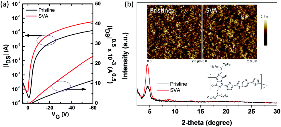 | ||
| Fig. 1 (a) Transfer characteristics of PDPPT-TT thin film transistors without and with solvent vapor annealing treatment. (b) XRD spectra of polymer thin films without and with solvent vapor annealing treatment (inset: AFM images of polymer thin films without and with solvent vapor annealing treatment and the chemical structure of PDPPT-TT). | ||
The dopant-free PDPPT-TT polymer was evaluated as a HTL in PSCs with the configuration FTO/TiO2/PCBM/MA1−yFAyPbI3−xClx/HTL/Ag (Fig. S1† shows the cross-sectional SEM image of the device). The energy band diagram of each layer in the device is shown in Fig. S2.† The device fabrication process is similar to our previously reported method.33 Compared to spiro-OMeTAD with a high concentration of 90–180 mg mL−1 in chlorobenzene and around 150–300 nm thickness, the PDPPT-TT polymer only uses a concentration of 3.0–5.0 mg mL−1 in chlorobenzene which produces a thickness of around 40–60 nm. Obviously, the PDPPT-TT polymer saves the device fabrication cost. Moreover, the PDPPT-TT polymer has a high charge carrier mobility and does not need any additional doping process involving Li salts or cobalt dopants, which could further simplify the fabrication process. The representative current density–voltage (J–V) curves and the corresponding device parameters are shown in Fig. 2 and Table 1. As shown in Fig. 2, the device with the pristine PDPPT-TT HTL exhibited an average PCE of 14.3%, a Voc of 1.02 V, a Jsc of 21.8 mA cm−2, and an FF of 0.65. The performance was similar to previously reported results.30,34 After appropriate solvent vapor annealing treatment, the average PCE of the device was significantly enhanced to 16.2%, Jsc and FF were enhanced to 22.6 mA cm−2, and 0.69, respectively, and Voc was slightly changed. The enhanced Jsc and FF should be caused by improved charge carrier extraction and collection due to the enhanced charge carrier mobility of PDPPT-TT as revealed by OTFT results. Moreover, the PCE and other parameters exhibited narrow distributions compared to those of devices based on the pristine PDPPT-TT polymer, indicating that the PDPPT-TT/perovskite has better interface contact after solvent vapor annealing. The champion device using the SVA treated PDPPT-TT HTL showed a Voc of 1.07 V, a Jsc of 22.8 mA cm−2, and an FF of 0.72, leading to a PCE of 17.8%. This value is likely to be among the highest values for perovskite solar cells based on the conjugated DPP polymer HTL. The thickness of the PDPPT-TT layer was also optimized by using different polymer solution concentrations. It was found that polymer solution concentrations less than 5 mg mL−1 decreased the device performance, while solution concentrations higher than 5 mg mL−1 could produce a discontinuous film due to the limited solubility of PDPPT-TT in chlorobenzene solvent (Fig. S3†). In comparison, the device based on the spiro-OMeTAD HTL with the dopant showed an average PCE of 15.8% with a Voc of 1.03 V, a Jsc of 22.1 mA cm−2, and an FF of 0.70. Furthermore, the device performance based on the doped spiro-OMeTAD HTL with additional solvent vapor treatment was also evaluated, and the device performance did not show any obvious improvement (Fig. S4†). Based on these results, it can be concluded that the conjugated polymers could be a better choice compared to the spiro-OMeTAD HTL due to their high mobility and dopant-free nature. The Jsc of the device was further checked by incident photon-to-current efficiency (IPCE) measurements. The absorption spectrum of PDPPT-TT is shown in Fig. S5.† Similar to previous reports, the PDPPT-TT polymer has weak absorption between 540 nm and 1000 nm. However, no IPCE peak over 800 nm wavelength could be observed, which confirmed that the PDPPT-TT polymer does not contribute to the current density since PDPPT-TT only acts as the hole transport layer.
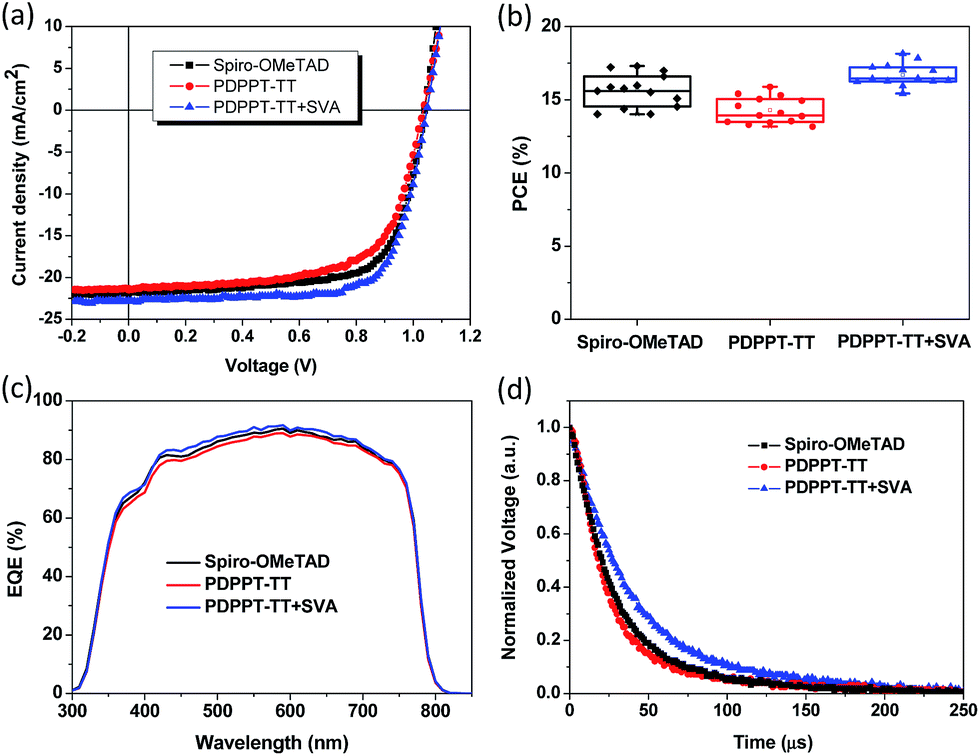 | ||
| Fig. 2 (a) J–V characteristics of PSCs based on the different HTLs. (b) Statistical distribution of solar cell efficiencies obtained from 16 devices based on the different HTLs. (c) IPCE spectra of PSCs based on the different HTLs. (d) TPV decay characteristics of PSCs based on the different HTLs. | ||
| Hole interlayer | V oc (V) | J sc (mA cm−2) | FF | PCE (%) [average] | PCE (%) [best] |
|---|---|---|---|---|---|
| Spiro-OMeTAD (doped) | 1.03 ± 0.02 | 22.1 ± 0.3 | 0.70 ± 0.02 | 15.8 ± 0.4 | 16.5 |
| PDPPT-TT | 1.02 ± 0.04 | 21.8 ± 0.6 | 0.65 ± 0.05 | 14.3 ± 0.6 | 15.8 |
| PDPPT-TT + SVA | 1.04 ± 0.02 | 22.6 ± 0.3 | 0.69 ± 0.02 | 16.2 ± 0.3 | 17.8 |
The device charge recombination dynamics behavior was characterized by using transient photovoltage (TPV) measurements. As shown in Fig. 2d, the spiro-OMeTAD HTL based device exhibited a carrier decay lifetime of 28.38 μs, and the device based on the PDPPT-TT HTL without any treatment showed a similar value (23.20 μs). However, the device based on the PDPPT-TT HTL after solvent vapor annealing treatment exhibited a much longer charge carrier lifetime of 38.90 μs than devices based on the other two layers, indicating a reduced charge carrier recombination. The higher charge carrier mobility and longer carrier decay lifetime are beneficial for efficient charge carrier transport and extraction, resulting in higher Jsc, FF and PCE than devices based on the other two HTLs.
The hysteresis and steady-state output curves of the PSCs based on the spiro-OMeTAD HTL and PDPPT-TT polymer with solvent vapour annealing treatment are shown in Fig. 3. The spiro-OMeTAD HTL based device exhibited significant hysteresis behaviour with a hysteresis index of 33.5% which is defined as (PCEreverse − PCEforward)/PCEreverse, while the PDPPT-TT HTL based device revealed negligible hysteresis behaviour (hysteresis index = 1.0%), which is similar to previously reported results.35 The steady-state output current density and PCE at the maximum power point are shown in Fig. 3b and d, respectively. The devices with spiro-OMeTAD and PDPPT-TT HTLs exhibited a stabilized PCE of 16.1% and 16.8%, respectively. One important note that needs to be mentioned is that the PDPPT-TT based device needs shorter time to stabilize compared to that with the spiro-OMeTAD HTL, indicating that the PDPPT-TT HTL has fewer charge trap states due to effective passivation between the HTL and the perovskite layer.36
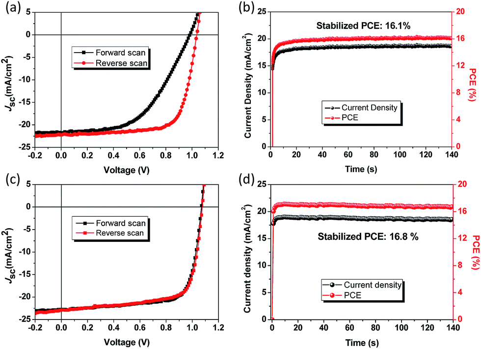 | ||
| Fig. 3 Hysteresis curves of solar cells based on spiro-OMeTAD (a), and PDPPT-TT (c) with solvent vapour annealing treatment. (b) Steady-state output curves of solar cells based on the spiro-OMeTAD HTL at a voltage bias of 0.87 V. (d) Steady-state output curves of solar cells based on the PDPPT-TT HTL at a voltage bias of 0.91 V. | ||
In order to investigate the charge transfer and extraction capability between the HTL and the perovskite layer, steady-state photoluminescence (PL) and time-resolved photoluminescence (TR-PL) measurements of perovskite films without or with the different HTLs on glass substrates were performed and the results are shown in Fig. 4. Compared to the PDPPT-TT polymer without solvent vapour annealing, the treated PDPPT-TT polymer significantly quenched the PL emission of the perovskite, indicating more efficient hole extraction at the perovskite/PDPPT-TT interface after solvent vapour annealing treatment due to improved film crystallinity and charge carrier mobilities. TR-PL measurements were also performed to confirm the charge transfer process at the perovskite/PDPPT-TT interface. As shown in Fig. 4 and Table S1,† after depositing the hole transporting interlayers, the perovskite film deposited on the spiro-OMeTAD HTL exhibited a PL lifetime of 12.53 ns after fitting to a two-exponential function, while the PL lifetimes were 20.45 ns and 13.90 ns for the perovskite/PDPPT-TT film before and after solvent vapour annealing treatment, respectively. The significantly reduced PL lifetime further confirms the efficient hole extraction at the perovskite/PDPPT-TT interface.
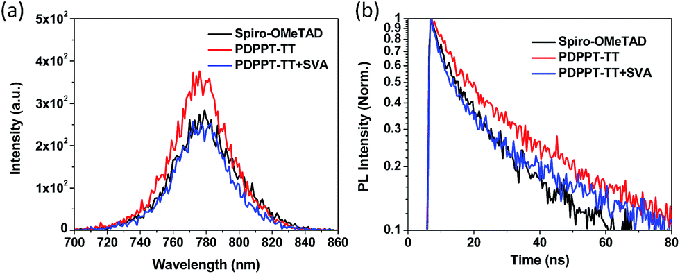 | ||
| Fig. 4 (a) Steady-state PL spectra of perovskite thin films deposited on the different HTLs. (b) TR-PL spectra of perovskite thin films deposited on the different HTLs. | ||
Finally, the device stability was also tested by storing the unencapsulated devices in air at room temperature with RH% of around 40% without excluding the room light. The devices were tested periodically over 72 hours under ambient air conditions (Fig. 5). As expected, the spiro-OMeTAD based cells exhibited a large decrease as the aging time increased. After 72 h of aging, the PCE decreased to 6.2% with a 40.7% retained efficiency compared to the initial value. This could be related to the hygroscopic properties of spiro-OMeTAD and dopants. The pristine PDPPT-TT HTL based device showed a similar performance degradation with a 26.7% retained efficiency. However, the PDPPT-TT with solvent annealing treatment based cells showed significantly enhanced stability. The PCE only slightly decreased to 56.5% after the same aging time. The device stability was improved after SVA treatment due to the improved film morphology and quality as confirmed by the above AFM and XRD results.24 We also performed a standard ageing test under illumination using ISOS-L1 protocols without excluding the UV-light. As shown in Fig. S6,† the T80 values which were defined as the time that corresponds to a drop of 20% of the initial efficiency were around 3.2 h, 4.0 h, and 5.4 h for devices based on spiro-OMeTAD and PDPPT-TT without and with solvent annealing treatment, respectively. The better stability of the PDPPT-TT based device may be due to the hydrophobic nature of the PDPPT-TT polymer which could prevent the water penetration into the perovskite surface. This result could be confirmed by the water contact angle measurements. As shown in Fig. S7,† a large contact angle of 103° for the PDPPT-TT polymer compared to 64° for spiro-OMeTAD further confirmed that the PDPPT-TT polymer has hydrophobic properties which could enhance the device stability as well.24,25
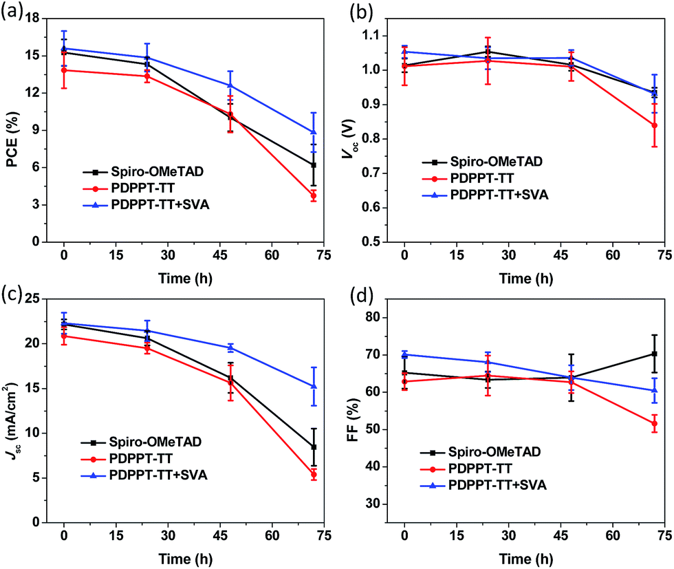 | ||
| Fig. 5 PCE (a), Voc (b), Jsc (c), and FF (d) parameters of the unencapsulated devices as a function of time under air conditions and a ∼40% humidity atmosphere. | ||
Experimental
Materials
All the materials, methylammonium iodide (MAI, 99.8%, Dyesol), formamidinium iodide (FAI, 99.8%, Dyesol), lead iodide (PbI2, 99.999%, Alfa), lead chloride (PbCl2, 99.999%, Alfa), N,N′-di-methylformamide (DMF, 99.8%, Aladdin), isopropanol (IPA, 99.5%, Sigma-Aldrich), titanium diisopropoxide bis(acetylacetonate) (75 wt% in isopropanol), titanium(IV) chloride (TiCl4, ≥98.0% purity), spiro-OMeTAD (Xi'an Polymer Light Technology Corp.), tris[2-(1H-pyrazol-1-yl)-4-tert-butylpyridine] cobalt(III) tris[bis-(turfluoromethylsuflonyl)imide] (FK209, Dyesol), bis-(trifluoromethane) sulfonimide lithium salt (LiTFSI, 96% purity, Sigma-Aldrich), 4-tBP (96% purity, Sigma-Aldrich), phenyl-C61-butyric acid methyl ester (PC61BM, 99%, ADS), C60-SAM (C60–COOH, 1-Materials), chlorobenzene (99.8%, Sigma), and tetrahydrofuran (THF), were used as received without further purification. The PDPPT-TT polymer was synthesised by a previously reported method with an Mn of 125k, an Mw of 359k, and a polydispersity index (PDI) of 2.7.27Device fabrication
The device fabrication process is similar to our previously reported method.33 Planar PSCs were fabricated on pre-patterned fluorine doped tin oxide (FTO) glass substrates (around 2 × 2.5 cm2 in size, 7 Ω per square). The FTO substrates were cleaned sequentially in detergent, deionized water, acetone, and ethanol in an ultrasonic bath for 20 min, respectively. Then, the FTO substrates were dried with nitrogen and treated in a UV ozone oven for 20 min. Then 0.15 M and 0.3 M compact TiO2 layer precursor solutions were prepared by adding 73.2 μL and 146.4 μL titanium diisopropoxide bis(acetylacetonate) 75 wt% in isopropanol (IPA) into 1 mL 1-butanol, respectively. The spin-coating procedure of the compact TiO2 layer was performed as follows: first, the 0.15 M precursor solution was spin coated on the FTO substrates at 4000 rpm for 45 s, and then the substrates were annealed on a hotplate in air at 150 °C for 5 min; the same process was repeated twice with a 0.3 M titanium diisopropoxide bis(acetylacetonate) solution. The as-prepared film was annealed at 450 °C for 15 min. After the substrates cooled down to room temperature, the TiO2 covered substrates were immersed in a 40 mM TiCl4 aqueous solution at 70 °C for 45 min and annealed at 450 °C for 15 min. Then, the samples were transferred into a nitrogen-filled glovebox and spin coated with a PC61BM solution (10 mg mL−1 in CB) at 6000 rpm for 45 s, followed by heating at 100 °C for 5 min. To make a uniform perovskite layer, 1.36 M PbI2 and 0.24 M PbCl2 were dissolved in DMF solvent, and stirred for 2 h at 75 °C. 70 mg MAI and 30 mg FAI were dissolved in 1 mL IPA with additional 10 μL DMF. After that, the PbX2 precursor solution was spin coated on top of the PC61BM covered substrates at 3000 rpm for 45 s, and then the solution of MAI and FAI was spin coated on top of the PbX2 substrates at 3000 rpm for 45 s. The samples were annealed at 100 °C for 10 min on a hotplate. During the annealing process, 40 μL IPA solvent was added around the substrates. Next, the spiro-OMeTAD or PDPPT-TT precursor solution was spin coated onto the perovskite layer at a spin rate of 3000 rpm for 45 s, and the spiro-OMeTAD/chlorobenzene (90 mg mL−1) precursor solution was employed with the addition of 45 μL 170 mg mL−1 lithium bis(trifluoromethylsulphonyl) imide (Li-TFSI) in acetonitrile, 75 μL 100 mg mL−1 FK209 in acetonitrile and 10 μL 4-tert-butylpyridine (tBP). Finally, 100 nm-thick Ag layers were thermally evaporated as the top electrodes. The area of the device was 0.075 cm2 defined by a shadow mask.The transistor fabrication followed our previously reported procedure.27 A heavily n-doped silicon wafer with a 200 nm thermal SiO2 layer was used as the substrate/gate electrode. The SiO2/Si substrate was cleaned with acetone and isopropyl alcohol (IPA), and then immersed in a piranha solution (H2SO4![[thin space (1/6-em)]](https://www.rsc.org/images/entities/char_2009.gif) :H2O2 = 2:1) for 8 minutes, followed by rinsing with deionized water. The OTS treatments were done by vapor treatment for 3 h at 120 °C in a vacuum. The semiconductor layer was deposited on top of the organosilane modified SiO2 surface by coating the semiconductor solution (DPPT-TT in CB solvent with a concentration of 4 mg mL−1) with a spin coater. The thin films were then solvent annealed for a suitable time. Subsequently, gold source/drain electrodes were deposited by thermal evaporation through a metal shadow mask to complete the TFTs with various channel lengths (L = 50–100 μm) and the same width (W = 1 mm). The TFT devices were then characterized using a Keithley SCS-4200 probe station in ambient air (dark).
:H2O2 = 2:1) for 8 minutes, followed by rinsing with deionized water. The OTS treatments were done by vapor treatment for 3 h at 120 °C in a vacuum. The semiconductor layer was deposited on top of the organosilane modified SiO2 surface by coating the semiconductor solution (DPPT-TT in CB solvent with a concentration of 4 mg mL−1) with a spin coater. The thin films were then solvent annealed for a suitable time. Subsequently, gold source/drain electrodes were deposited by thermal evaporation through a metal shadow mask to complete the TFTs with various channel lengths (L = 50–100 μm) and the same width (W = 1 mm). The TFT devices were then characterized using a Keithley SCS-4200 probe station in ambient air (dark).
Measurements and characterization
All current density–voltage (J–V) curves were recorded using a Keithley 2400 source meter unit under simulated AM 1.5 G illumination at an intensity of 100 mW cm−2 with an XES-70S1 solar simulator. The system was calibrated using an NREL-certified monocrystal Si photodiode detector before device testing. The morphology measurement of the perovskite layers was measured by scanning electron microscopy (SEM) (JSM-7800F). An X-ray diffraction (XRD) test was conducted on a Bruker D8 Advance XRD instrument. The UV-visible absorption spectra were measured on a Perkin-Elmer Lambda 950 spectrophotometer. The samples were prepared by the same device fabrication process. The incident photon-to-current conversion efficiency (IPCE) spectra were recorded using a solar cell quantum efficiency measurement system (SCS10-X150, Zolix Instrument. Co. Ltd). Steady photoluminescence (PL) and time-resolved photoluminescence (TR-PL) were measured by using a Pico Quant Fluotime 300 with a 510 nm picosecond pulsed laser. Transient photocurrent (TPC) measurements were performed with a system excited by a 532 nm (1000 Hz, 3.2 ns) pulse laser. Transient photovoltage (TPV) measurements were performed with the same system excited by a 405 nm (50 Hz, 20 ms) pulse laser. A digital oscilloscope (Tektronix, D4105) was used to record the photocurrent or photovoltage decay process with a sampling resistance of 50 Ω or 1 MΩ, respectively. All the measurements of the solar cells were performed under an ambient atmosphere at room temperature without encapsulation.Conclusions
In conclusion, PSCs with conjugated polymer HTLs showed superior device performance and stability after appropriate solvent vapor annealing treatment compared to the device with the most commonly used spiro-OMeTAD HTL. The performance is among the best for PSCs with a dopant-free conjugated polymer based HTL. Meanwhile, the PDPPT-TT polymer exhibited a lower cost and simpler fabrication process, making it a beneficial candidate for future low cost high performance perovskite based energy devices. More importantly, this study provides an approach for employing the most studied conjugated polymer as the HTL in PSCs.Conflicts of interest
There are no conflicts to declare.Acknowledgements
This work was financially supported by the National Natural Science Foundation of China (61604119 and 61704131), the Natural Science Foundation of Shaanxi Province (2017JQ6002 and 2017JQ6031), the Fundamental Research Funds for the Central Universities, and the Young Elite Scientists Sponsorship Program by CAST.Notes and references
- NREL, National Renewable Energy Laboratory Chart, www.nrel.gov/ncpv/images/efficiency_chart.jpg, 2018 Search PubMed.
- W. Chen, Y. Wu, Y. Yue, J. Liu, W. Zhang, X. Yang, H. Chen, E. Bi, I. Ashraful, M. Gratzel and L. Han, Science, 2015, 350, 944–948 CrossRef PubMed.
- S. S. Shin, E. J. Yeom, W. S. Yang, S. Hur, M. G. Kim, J. Im, J. Seo, J. H. Noh and S. Il Seok, Science, 2017, 356, 167–171 CrossRef PubMed.
- M. Saliba, T. Matsui, K. Domanski, J.-Y. Seo, A. Ummadisingu, S. M. Zakeeruddin, J.-P. Correa-Baena, W. R. Tress, A. Abate, A. Hagfeldt and M. Gratzel, Science, 2016, 354, 206–209 CrossRef PubMed.
- L. Zhou, J. Chang, Z. Liu, X. Sun, Z. Lin, D. Chen, C. Zhang, J. Zhang and Y. Hao, Nanoscale, 2018, 10, 3053–3059 RSC.
- N. J. Jeon, H. G. Lee, Y. C. Kim, J. Seo, J. H. Noh, J. Lee and S. Il Seok, J. Am. Chem. Soc., 2014, 136, 7837–7840 CrossRef PubMed.
- W. H. Nguyen, C. D. Bailie, E. L. Unger and M. D. McGehee, J. Am. Chem. Soc., 2014, 136, 10996–11001 CrossRef PubMed.
- Z. Li, J. Tinkham, P. Schulz, M. Yang, D. H. Kim, J. Berry, A. Sellinger and K. Zhu, Adv. Energy Mater., 2017, 7, 1601451 CrossRef.
- J. Seo, N. J. Jeon, W. S. Yang, H. W. Shin, T. K. Ahn, J. Lee, J. H. Noh and S. Il Seok, Adv. Energy Mater., 2015, 5, 1–6 Search PubMed.
- S. Wang, W. Yuan and Y. S. Meng, ACS Appl. Mater. Interfaces, 2015, 7, 24791–24798 CrossRef PubMed.
- H. Xi, S. Tang, X. Ma, J. Chang, D. Chen, Z. Lin, P. Zhong, H. Wang and C. Zhang, ACS Omega, 2017, 2, 326–336 CrossRef.
- E. J. Juarez-Perez, M. R. Leyden, S. Wang, L. K. Ono, Z. Hawash and Y. Qi, Chem. Mater., 2016, 28, 5702–5709 CrossRef.
- W. Zhou, Z. Wen and P. Gao, Adv. Energy Mater., 2018, 8, 1702512 CrossRef.
- J. You, L. Meng, T.-B. Song, T.-F. Guo, Y. Yang, W.-H. Chang, Z. Hong, H. Chen, H. Zhou, Q. Chen, Y. Liu, N. De Marco and Y. Yang, Nat. Nanotechnol., 2015, 11, 75–81 CrossRef PubMed.
- Z. Liu, J. Chang, Z. Lin, L. Zhou, Z. Yang, D. Chen, C. Zhang, S. F. Liu and Y. Hao, Adv. Energy Mater., 2018, 1703432 CrossRef.
- T. Swetha and S. P. Singh, J. Mater. Chem. A, 2015, 3, 18329–18344 RSC.
- C. Rodríguez-Seco, L. Cabau, A. Vidal-Ferran and E. Palomares, Acc. Chem. Res., 2018, 51, 869–880 CrossRef PubMed.
- Y. S. Kwon, J. Lim, H.-J. Yun, Y.-H. Kim and T. Park, Energy Environ. Sci., 2014, 7, 1454 RSC.
- P. Qin, H. Kast, M. K. Nazeeruddin, S. M. Zakeeruddin, A. Mishra, P. Bäuerle and M. Grätzel, Energy Environ. Sci., 2014, 7, 2981 RSC.
- J. Lee, M. Malekshahi Byranvand, G. Kang, S. Y. Son, S. Song, G. W. Kim and T. Park, J. Am. Chem. Soc., 2017, 139, 12175–12181 CrossRef PubMed.
- G. W. Kim, J. Kim, G. Y. Lee, G. Kang, J. Lee and T. Park, Adv. Energy Mater., 2015, 5, 1–8 Search PubMed.
- W. Chen, X. Bao, Q. Zhu, D. Zhu, M. Qiu, M. Sun and R. Yang, J. Mater. Chem. C, 2015, 3, 10070–10073 RSC.
- J. W. Jo, M. Seo, M. Park, J. Kim, J. S. Park, I. K. Han, H. Ahn, J. W. Jung, B. Sohn, M. J. Ko and H. J. Son, Adv. Funct. Mater., 2016, 26, 4464–4471 CrossRef.
- H.-C. Liao, T. L. D. Tam, P. Guo, Y. Wu, E. F. Manley, W. Huang, N. Zhou, C. M. M. Soe, B. Wang, M. R. Wasielewski, L. X. Chen, M. G. Kanatzidis, A. Facchetti, R. P. H. Chang and T. J. Marks, Adv. Energy Mater., 2016, 6, 1600502 CrossRef.
- G.-W. Kim, G. Kang, J. Kim, G.-Y. Lee, H. Il Kim, L. Pyeon, J. Lee and T. Park, Energy Environ. Sci., 2016, 9, 2326–2333 RSC.
- P. Sonar, J. Chang, J. H. Kim, K.-H. Ong, E. Gann, S. Manzhos, J. Wu and C. R. McNeill, ACS Appl. Mater. Interfaces, 2016, 8, 24325–24330 CrossRef PubMed.
- J. Chang, Z. Lin, J. Li, S. L. Lim, F. Wang, G. Li, J. Zhang and J. Wu, Adv. Electron. Mater., 2015, 1, 1500036 CrossRef.
- J. Chang, P. Sonar, Z. Lin, C. Zhang, J. Zhang, Y. Hao and J. Wu, Org. Electron., 2016, 36, 113–119 CrossRef.
- S. Jeon, U. K. Thakur, D. Lee, Y. Wenping, D. Kim, S. Lee, T. K. Ahn, H. J. Park and B. Kim, Org. Electron., 2016, 37, 134–140 CrossRef.
- A. Dubey, N. Adhikari, S. Venkatesan, S. Gu, D. Khatiwada, Q. Wang, L. Mohammad, M. Kumar and Q. Qiao, Sol. Energy Mater. Sol. Cells, 2016, 145, 193–199 CrossRef.
- K. C. Dickey, J. E. Anthony and Y.-L. Loo, Adv. Mater., 2006, 18, 1721–1726 CrossRef.
- X. Sun, C. Zhang, J. Chang, H. Yang, H. Xi, G. Lu, D. Chen, Z. Lin, X. Lu, J. Zhang and Y. Hao, Nano Energy, 2016, 28, 417–425 CrossRef.
- J. Ma, J. Chang, Z. Lin, X. Guo, L. Zhou, Z. Liu, H. Xi, D. Chen, C. Zhang and Y. Hao, J. Phys. Chem. C, 2018, 122, 1044–1053 CrossRef.
- Y. S. Kwon, J. Lim, H.-J. Yun, Y.-H. Kim and T. Park, Energy Environ. Sci., 2014, 7, 1454 RSC.
- I. Levine, P. K. Nayak, J. T. Wang, N. Sakai, S. Van Reenen, T. M. Brenner, S. Mukhopadhyay, H. J. Snaith, G. Hodes and D. Cahen, J. Phys. Chem. C, 2016, 120, 16399–16411 CrossRef.
- Y. Shao, Z. Xiao, C. Bi, Y. Yuan and J. Huang, Nat. Commun., 2014, 5, 5784 CrossRef PubMed.
Footnote |
| † Electronic supplementary information (ESI) available: UV-vis absorption spectrum of PDPPT-TT, water contact angle measurements, and fitted decay times of the perovskite thin films. See DOI: 10.1039/c8se00233a |
| This journal is © The Royal Society of Chemistry 2018 |