
Influence of doped charge transport layers on efficient perovskite solar cells†
Jorge
Avila
 a,
Lidon
Gil-Escrig
b,
Pablo P.
Boix
a,
Michele
Sessolo
a,
Steve
Albrecht
*b and
Henk J.
Bolink
*a
a,
Lidon
Gil-Escrig
b,
Pablo P.
Boix
a,
Michele
Sessolo
a,
Steve
Albrecht
*b and
Henk J.
Bolink
*a
aInstituto de Ciencia Molecular, Universidad de Valencia, C/J. Beltrán 2, 46980, Paterna, Spain. E-mail: henk.bolink@uv.es
bHelmholtz-Zentrum Berlin für Materialien und Energie GmbH, Young Investigator Group for Perovskite Tandem Solar Cells, Kekuléstraße 5, 12489 Berlin, Germany. E-mail: steve.albrecht@helmholtz-berlin.de
First published on 3rd July 2018
Abstract
Planar vacuum deposited p–i–n methyl ammonium lead tri-iodide perovskite solar cells are prepared with different electron and hole transporting layers, either doped or undoped. The effect of these layers on the solar cells performance (efficiency and stability) is studied. The main benefit of using doped layers lies in the formation of barrier free charge extraction contacts to the electrodes. However, this comes at the cost of increased residual absorption (reducing the current density and efficiency of the cells) and a decreased stability. A generic solar cell structure using undoped charge extraction layers is presented, containing a thin layer of a strong electron acceptor in between the transparent electrode and the hole transport layer, that leads to efficiencies of 18% and a significant (>5 times) improvement of the stability.
Introduction
Metal halide perovskite solar cells have become the most promising renewable power source.1–4 The potential of this technology is evidenced by the rapid improvement in efficiency, reaching record values of 22.7%.5 In the majority of the reported perovskite solar cells the absorber layer is sandwiched in between charge selective transport layers.6 These layers have to ensure rectification which is essential to achieve high open circuit voltages (Voc's).7 Additionally, these layers have to transport and inject the selected carrier to the contact, thus their conductivity is frequently enhanced by “doping” them with additives that lead to excess charges in the layers.8 Probably the most prominent example is the hole transport layer (HTL) based on partially oxidized (doped) spiro-OMeTAD.9 The benefit of using doped layers is a reduced series resistance and the formation of ohmic contacts to the external electrodes, which enhances the solar cell fill factor. One drawback of the use of doped charge transport layers is their negative effect on the device lifetime.10 The above mentioned generality is found in particular for solar cells employing perovskite layers that are solution processed.11,12 Much less information is available for solar cells employing perovskite films prepared using a dry vapor based deposition process. In a recent report, it was demonstrated that the use of doped charge transport layers is also beneficial for the performance of vacuum deposited perovskite solar cells.13 In that case, however, it was shown to be essential to prevent a direct contact between the perovskite absorber and the doped layers, which would otherwise results in substantial charge recombination. For this reason, a thin layer of the pure (undoped) organic charge transport molecules was inserted in between the doped charge transport layer and the perovskite absorber.13 Similar effects are known from work with organic light-emitting diodes and photovoltaic devices were such non-doped layers prevent the quenching of excitons.8 It is likely that for perovskite solar cells the elimination of the doped layers adjacent to the perovskite reduces charge recombination and enhances the device performance due to improved rectification, as was recently also mentioned in another study.14 Besides this there are other drawbacks associated to the doping of the contacts. On the one hand, the stability of solar cells using doped layers is generally below that of those employing non-doped charge transport layers; on the other, doping generally enhances parasitic absorption. This is in particular the case when arylamine containing molecules (which are common hole transport materials) are partially oxidized by the dopants. The radical cation of arylamines has a characteristic optical absorption band in the visible region of the spectrum in the 500–600 nm range.15 Hence, this reduces the light that reaches the perovskite layer and hence the achievable current density the cells can produce. This is of some importance in the n–i–p configuration (that is with the electron transporting layer, ETL, on the illuminated side of the cell and the hole transporting layer behind the perovskite layer) as the amount of reflected sunlight from the metal top electrode is reduced. However, this parasitic absorption is more prominent when the sunlight passes through the doped hole transport layer prior to reaching the perovskite absorber, in the so-called p–i–n configuration. It is therefore, of interest to prepare p–i–n type perovskite solar cells, that do not require doped hole transport layers (HTLs) yet do provide efficient charge extraction to the transparent front electrode as this is expected to increase the current density and hence the PCE of the devices. At the same time, it is also of interest to eliminate the doped electron transport layer (ETL) placed on top of the perovskite absorber layer as this may lead to improved stabilities.Here, we study the influence of the doped and undoped transport layers on the performance and stability of thin film perovskite solar cells in the p–i–n configuration. The p–i–n configuration was selected as the parasitic absorption in doped p-type layers is higher than in doped n-type layers. Methyl ammonium lead tri-iodide (MAPbI3) prepared via co-sublimation of its precursors was used as the perovskite absorber. An intrinsic advantage of vacuum deposition is the possibility to selectively remove and exchange any layer and study the effect on the overall device performance. It was found that the ITO- undoped-HTL interface is preventing efficient charge extraction which was overcome by the insertion of a thin layer of the molecule used to oxidize the hole transport molecule, 2,2′-(perfluoronaphthalene-2,6-diylidene)di-malononitrile (F6-TCNNQ) (Fig. 1) in between the ITO and the HTL. The doped ETL is replaced by a bilayer of 2,9-dimethyl-4,7-diphenyl-1,10-phenanthroline (BCP) (Fig. 1) and Ag. Using this approach, the power conversion efficiency of the p–i–n solar cells is enhanced to more than 18%, whereas at the same time the stability is notably improved.
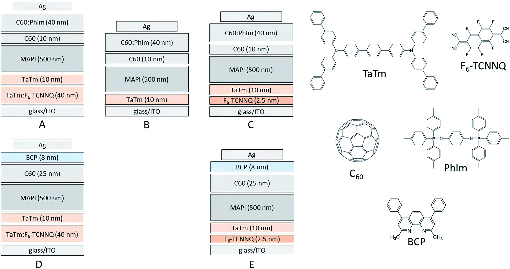 | ||
| Fig. 1 Layout of the studied devices, A, B, C, D and E each one with a different combination of doped and undoped transport layers and chemical structures of the transport materials. | ||
The MAPbI3 perovskite thin films were prepared by co-evaporation of the two starting compounds, CH3NH3I and PbI2. Details of the experimental conditions for the perovskite layer have been described previously and are presented in the ESI.†16 Out of the two perovskite precursors, CH3NH3I and PbI2, the first is somewhat complicated to sublime. However, once properly outgassed (using the high vacuum of the evaporation chamber) the material is sublimed similarly like small molecular weight organic molecules, that is, the rate of evaporation is stable as monitored by the microbalance crystal sensors that are positioned in the chamber. These films were characterized using grazing incidence X-ray diffraction (GIXRD) showing the typical diffraction pattern for this material which is independent on the type of organic under-layer employed (Fig. S1a in the ESI†). Scanning electron microscopy (SEM) images of the perovskite surface (Fig. S1c in the ESI†) show a dense packing of crystals, virtually without pinholes, that have an average domain size of approximately 100 nm. Note that the domain size here is not depending on the type of under-layer employed. The optical absorption spectra of these films show the expected MAPbI3 band-to-band transition at 780 nm and high absorbance over the whole visible spectra (Fig. S1b in the ESI†). These perovskite layers were used to prepare planar diodes by sandwiching a 500 nm thick perovskite layer in between organic HTLs and ETLs, the first on top of a pre-patterned indium tin oxide (ITO) coated glass substrate and by thermally evaporating a metal top contact on the latter. A vacuum deposited MAPbI3 layer with a thickness of 500 nm was selected as previous studies showed that almost all sun light with energy above the band-gap is absorbed and still all charge carriers can reach the respective interfaces without significant transport losses within the absorber layer.17 Both the electron selective and hole selective organic charge transport layers were prepared by vacuum sublimation of the corresponding organic molecules to a layer thickness of 10 nm. We selected a derivative of an arylamine, N4,N4,N4′′,N4′′-tetra([1,1′-biphenyl]-4-yl)-[1,1′:4′,1′′-terphenyl]-4,4′′-diamine (TaTm) (Fig. 1) as the hole transport molecule due to its very stable sublimation conditions and tendency to form completely amorphous films. The fullerene C60 was selected as the electron transport molecule as it is also easy to sublime and has proven to be an efficient electron acceptor in perovskite solar cells.18 To ensure sufficient statistics, for each device configuration mentioned in this report, at least 2 different substrates each containing 4 cells were evaluated, while for top performing configurations at least 5 different substrates with a total of 20 cells were characterized. The device area used, defined as the aperture of the shadow mask, was 1 mm2, whereas the overlap area between front and back electrode was 4 mm2. This configuration was used to make sure the performance of the cell is not overestimated although it leads to a slight underestimation of the Voc.19 Doping of the HTL was achieved by co-evaporating the molecule F6-TCNNQ with the TaTm at a ratio TaTm![[thin space (1/6-em)]](https://www.rsc.org/images/entities/char_2009.gif) :F6-TCNNQ of 11% as determined by the microbalance crystal sensor evaporation rate monitors. Doping of the C60 layer was achieved by co-evaporating the molecule N1,N4-bis(tri-p-tolylphosphoranylidene)-benzene-1,4-diamine (PhIm) (Fig. 1) at a ratio C60:PhIm of 30% as determined by the microbalance crystal sensor evaporation rate monitors. More details of the fabrication process can be found in the ESI.†
:F6-TCNNQ of 11% as determined by the microbalance crystal sensor evaporation rate monitors. Doping of the C60 layer was achieved by co-evaporating the molecule N1,N4-bis(tri-p-tolylphosphoranylidene)-benzene-1,4-diamine (PhIm) (Fig. 1) at a ratio C60:PhIm of 30% as determined by the microbalance crystal sensor evaporation rate monitors. More details of the fabrication process can be found in the ESI.†
Five different types of devices were prepared and evaluated which are depicted in Fig. 1 and named A, B, C, D and E, respectively. Device A is the reference in which both a doped HTL and a doped ETL are used. In device B, the doped HTL is removed and the TaTm layer is in direct contact with the ITO front electrode. Device C is similar to device B, but a thin (2.5 nm) layer of the molecule F6-TCNNQ is deposited on top of the ITO prior to depositing the HTL. In device D and E, the configuration on the p-contact side is copied from device A and C, whereas the doped C60 layer is substituted by a thin layer (8 nm) of BCP. Such an ETL approach (C60/BCP/Ag) has been used in organic photovoltaics,20 and was also adopted to perovskite solar cells.21 All devices use an Ag top electrode of 100 nm.
As discussed before, the perovskite film properties are very similar for all type of devices, which is expected as in all cases it is formed directly on top of the TaTm HTL. Furthermore, the different device configurations were prepared in a single perovskite sublimation run, ensuring that the perovskite layer is identical for all these devices (the best performing device configurations were then also prepared separately to obtain more statistics). The dark current density–voltage (J–V) curves of the finished diodes are depicted in Fig. 2 and show low leakage current in all cases as well as a steep rise of the current density at ∼0.5 V. This implies that the layer quality is good and even though thin charge selective layers are used this does not lead to shunts in the diode. For device B, however, this rise in current density is much less pronounced. As the only difference is the interface this result implies that there is a barrier for hole-injection in this device type. Additionally, device A, with doped HTL and doped ETL shows a higher leakage current, in line with the higher conductivity of these layers.
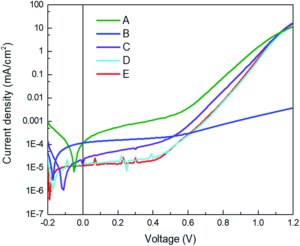 | ||
| Fig. 2 Typical current density versus voltage characteristics for the series of devices in the dark. | ||
Using AM 1.5G simulated sun illumination at an intensity of 100 mW cm−2 the J–V curves of the different cells were again determined. These J–V curves under illumination are depicted in Fig. 3a, both in forward and backward scan direction. For all type of devices there is very little hysteresis in the J–V curves and is therefore considered negligible here. The reference device, A, performs similar as reported previously,13 reaching for the best cell; Jsc of 20.7 mA cm−2, a Voc of 1.08 V and a fill factor (FF) of 72%, leading to a PCE of 16.2%. When the doped HTL is removed, referred to as device B, the J–V curve under illumination shows a low fill factor with a pronounced S-shape, indicating issues with charge extraction and injection. This corroborates the conclusion drawn from the dark J–V curves. The only difference between device A and B is the removal of the doped layer at the ITO/HTL interface hence, the origin for the poor J–V curves must originate from that interface. This is not unexpected in view of the large energy offset between the work function of ITO (4.8 eV) and the highest occupied molecular orbital (HOMO) of TaTm (5.4 eV). This and the J–V results, clearly indicate that the contact between ITO and TaTm is not without a barrier. Hence, to alleviate this and ensure a barrier-free charge extraction, a thin layer (2.5 nm) of the F6-TCNNQ was deposited on top of the ITO prior to the deposition of the TaTm (device C). As can be seen from Fig. 3, the J–V curve of this type of device (type C) is again approaching a rectangular shape (FF = 79%) indicating that the extraction barrier has been removed. Additionally, the Jsc of device C is substantially increased when compared with that of device A. This effect can be understood when comparing the EQE graphs of the different devices (Fig. 3b) where device C has an enhanced spectral response in the blue-green region of the solar spectrum. Even though it is probable that at the interface between the 2.5 nm of F6-TCNNQ and TaTm a small fraction of TaTm molecules gets oxidized (ensuring a good electrical contact between them) this does not lead to a very pronounced increase in the absorption of the film. The spontaneous transfer of an electron from the TaTm to the F6-TCNNQ layer upon contact between the two leads to excess electrons in the LUMO of the F6-TCNNQ and holes in the HOMO of the TaTm. The excess electrons in the LUMO are responsible for the formation of the ohmic contact between the ITO electrode and F6-TCNNQ layer. In Fig. 4 the absorption and transmission of the two types of HTL are depicted. These layers were prepared on glass substrates and consisted of TaTm:F6-TCNNQ (40 nm)/TaTm (10 nm) and F6-TCNNQ (2.5 nm)/TaTm (10 nm) resembling the stack in device A and C respectively. Indeed, there is a substantial decrease in the absorption spectrum for the HTL double layer of device C when compared to that of the reference device (A). The reduction in the visible part of the spectrum is primarily due to the absence of the absorption band around 500 nm. This reduction in the parasitic absorption leads to more light reaching the perovskite, which therefore explains the increase in Jsc for this configuration. Moreover, the bi-layer type HTL used in device C shows excellent transmittance up to 1300 nm, which makes it a valuable option for use in tandem applications with low bandgap absorbers such as silicon.
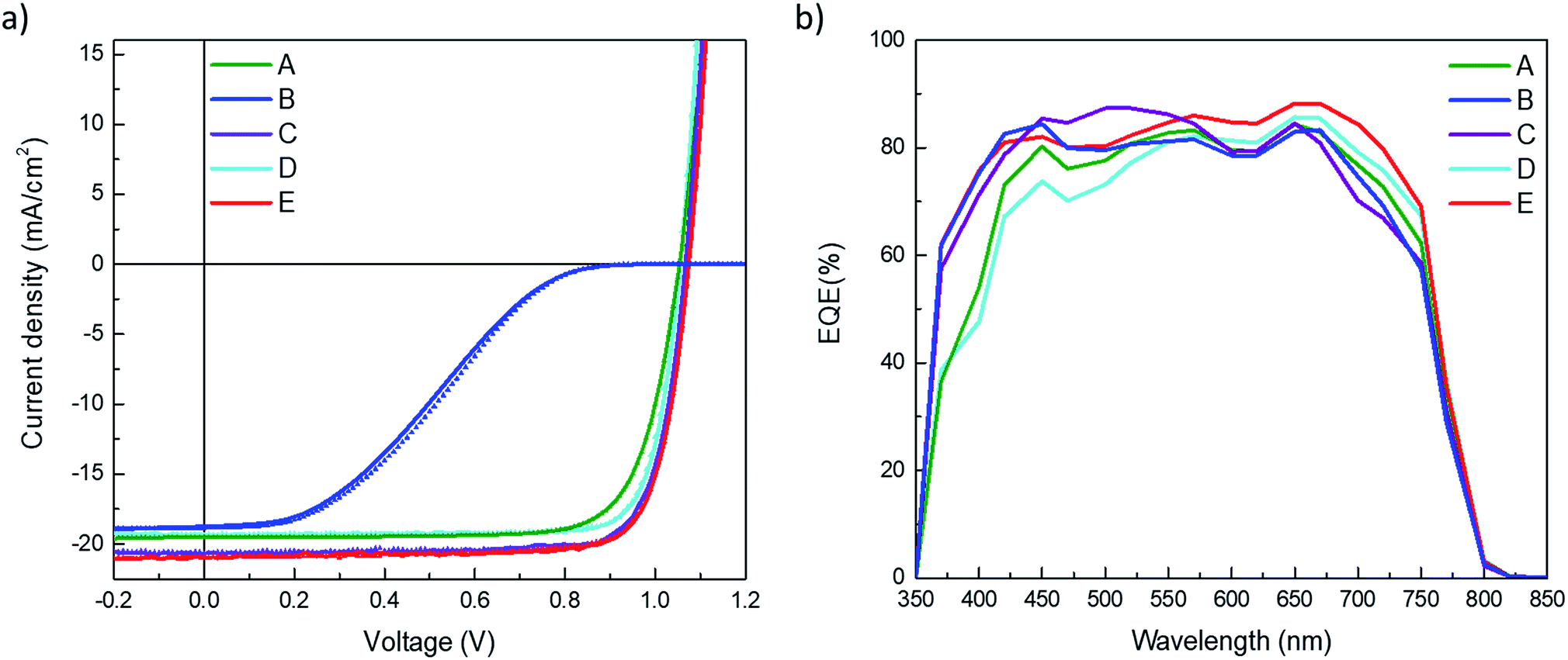 | ||
| Fig. 3 (a) Representative J–V characteristics measured under simulated AM 1.5G-illumination in forward (dotted line) and reverse (straight line) scan direction for each studied device. (b) External quantum efficiency (EQE) spectra for the same device series. | ||
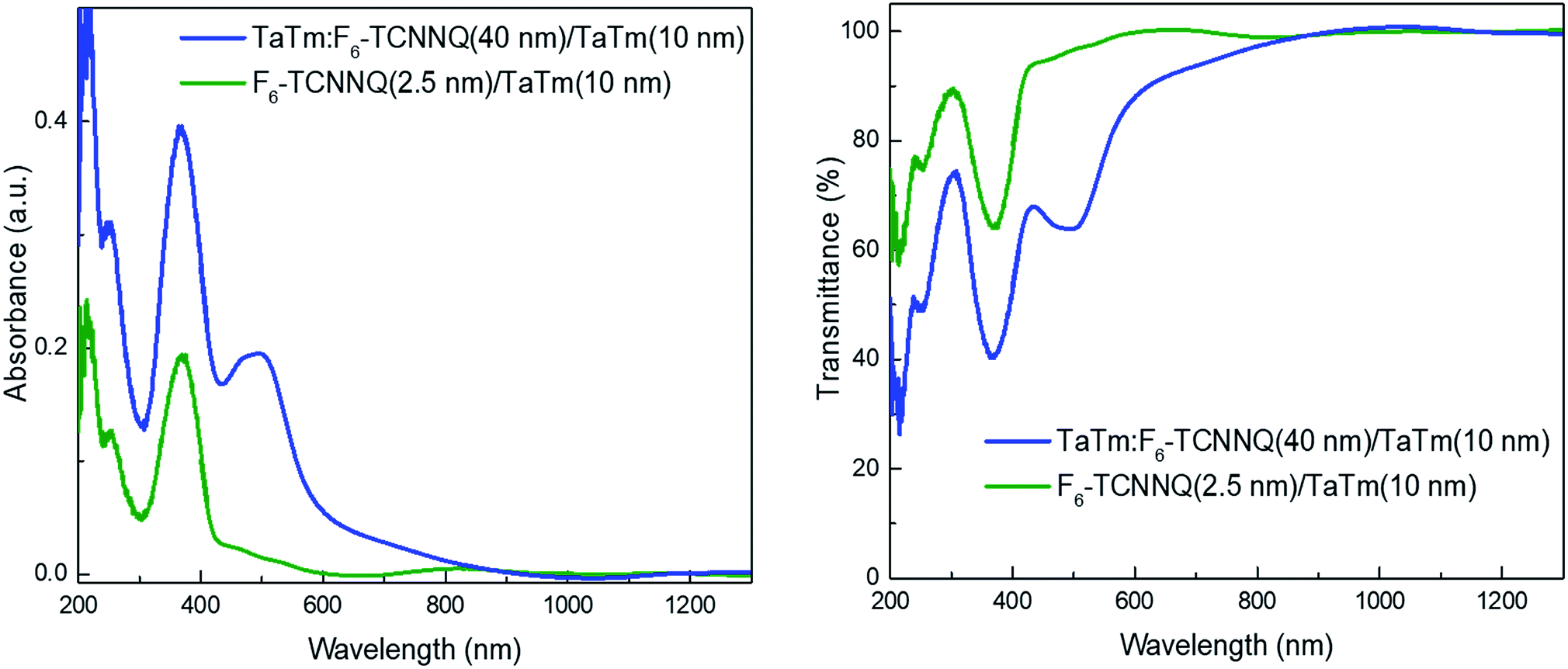 | ||
| Fig. 4 Absorbance (left) and transmission (right) spectra of the hole transport layers for devices A, D and C, E, blue and green lines, respectively. | ||
Device type D and E, have similar Jsc and Voc as device A and C. The similar Jsc's are expected as the front contacts are unvaried and the effect of the top charge transport layer on the optical absorption is small. This is due to the use of the thick perovskite layer which absorbs virtually all the sun-light in the first pass. There is a small improvement in the FF for device D when compared to device A. This may be due to an increased rectification and or charge extraction for the C60/BCP/Ag stack.
An overview of the key performance indicators for all type of devices is depicted in Table 1 (record values) and the statistics of each device type is shown in Fig. S2 in the ESI.† As device B, was not performing well, for this configuration only a few cells were prepared.
| PCE (%) | J sc (mA cm−2) | V oc (mV) | FF (%) | |
|---|---|---|---|---|
| A | 16.2 | 20.8 | 1076 | 72.5 |
| B | 5.4 | 18.8 | 1032 | 27.9 |
| C | 17.9 | 21.3 | 1056 | 79.4 |
| D | 16.9 | 19.6 | 1052 | 81.7 |
| E | 18.2 | 21.3 | 1059 | 80.4 |
To obtain an indication of the stabilities of the different cell configurations they were analyzed during prolonged exposure to white LED light (spectra in Fig. S3 in the ESI†), except for the moderately performing device B. The light intensity was adjusted to mimic the Jsc value obtained under AM 1.5G illumination. The temperature of the cells during this test reached approximately 40 °C in the first 10 minutes and remained constant afterwards. The setup consisted of 8 test positions installed inside a nitrogen filled glovebox (with oxygen and H2O levels below 1 ppm). All cells were continuously illuminated under short-circuit conditions without encapsulation and evaluated within a few days after preparation. At fixed time intervals (1 hour, initially) J–V scans were taken to deduce the evolution of the key performance indicators of the cells, including the PCE (Fig. S4 in the ESI†). This type of ageing experiment provides an indication of the stability. Maximum power point tracking is the preferred way of determining the stability of the cells as it most closely resembles real operation conditions. However, considering the negligible hysteresis of the analyzed devices, this type of measurement gives additional information. In particular, it allows to determine which parameter is causing the power efficiency decay allowing to postulate possible degradation mechanisms. Some examples of the J–V scans for each device configuration at set times of operation under constant illumination are depicted in Fig. S5.† The evolution of the performance parameters over time are depicted in Fig. 5 and the zoomed in version in Fig. S4.† We can distinguish two types of behavior for the different devices. The device types D and E, both having the C60/BCP/Ag ETL stack, are stable over more than 280 hours under continuous illumination, with only a decrease of ∼10% of the PCE. This reduction is mainly due to a drop in Jsc. Interestingly, the Voc increases slightly over the first 100 hours, which we postulate is due to the passivation of trap states at the interface between the perovskite and the organic charge extraction layers. A very different behavior is observed for the devices of type A and C that employ the C60/C60:PhIm layer as the ETL stack. These two types of devices are less stable and after approximately 100 hours a reduction in the PCE to 80% has already taken place. The decay in these cases appears to be driven by all the parameters and especially by the Jsc and the FF which drop faster than in the devices with undoped electron transport layers. These results indicate that the deterioration of these cells is related to an increase in the series resistance which is likely to be related to the ETL as both devices have only this layer in common. It is possible that de-doping of the C60 layer occurs as this layer is only protected by a sublimed (not-pinhole free) metal electrode which would lead to an extraction barrier at the metal interface, decreasing the stability of the devices considerably. This degradation also leads to S-shaped J–V curves. It is important to note that in all these devices the perovskite layer is the same, a vacuum deposited MAPbI3 layer, which implies that with the proper contacts these devices can be rather stable.
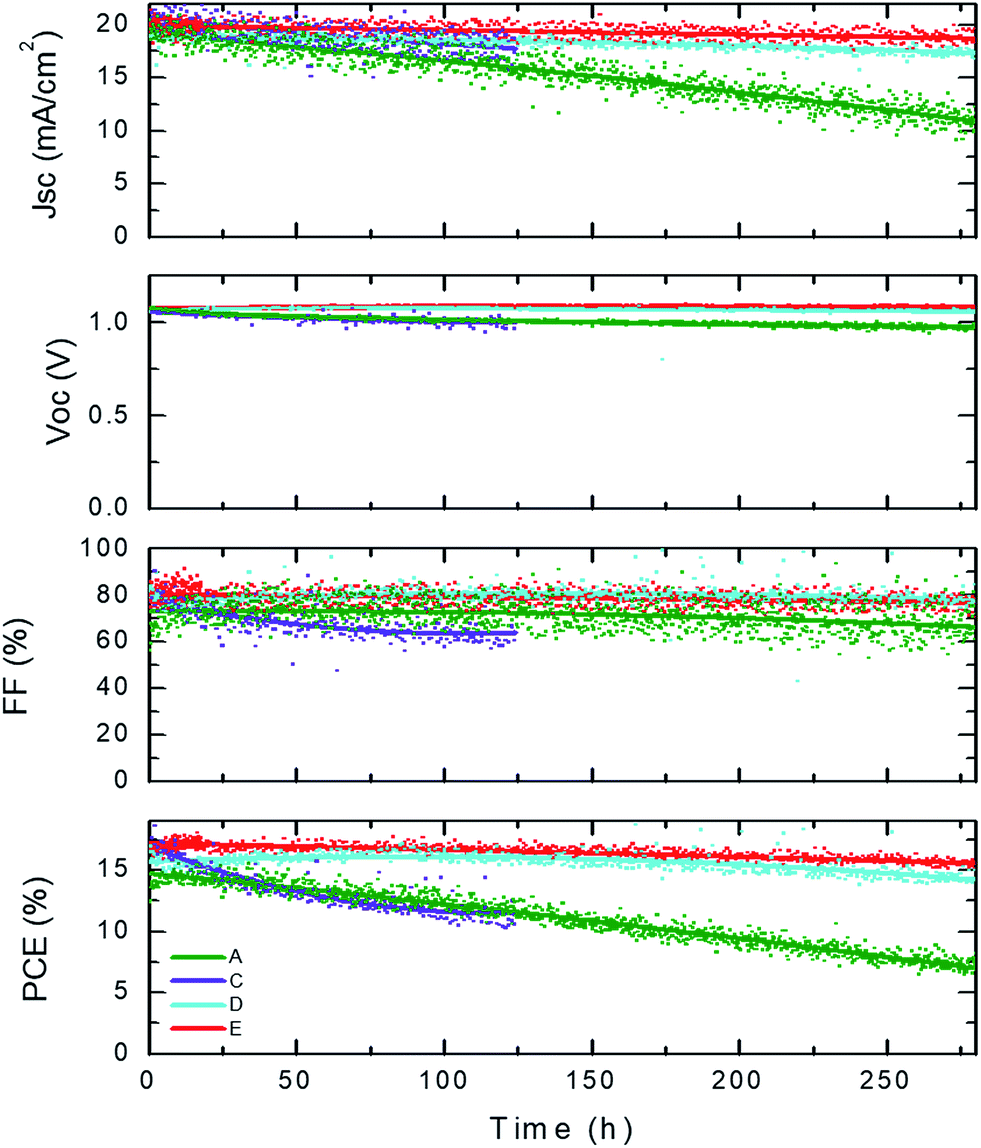 | ||
| Fig. 5 J–V characteristic parameters versus time measured under continuous LED illumination in inert atmosphere. Device are maintained at short circuit conditions and each hour a JV scan is performed. | ||
Conclusions
In conclusion the performance and stability of planar p–i–n perovskite solar cells is significantly enhanced when the doped charge transport layers are replaced by undoped alternatives. When substituting the doped hole transport layer with an undoped equivalent it was found that a charge injection/extraction barrier is present at the ITO-HTL interface. This was eliminated by inserting a very thin layer of the pure dopant molecule in between the ITO and the HTL. The main benefit of using undoped HTL in the p–i–n configuration is the strong reduction of the parasitic absorption. This leads to an enhancement of the spectral response in the blue part of the solar spectrum and hence to an increase in the current density. The elimination of reactive electron transport layers on top of the perovskite results in a significant increase in the solar cell stability. Interestingly, the bilayer C60/BCP ETL lead to diodes with high rectifications comparable to the much more conductive C60/C60-PhIm layer, as evidenced by the high FF obtained. The generic architectures identified here can yield very efficient and rather stable solar cells, and might be used in a wide range of planar type perovskite solar cells and multi-junction architectures.Conflicts of interest
There are no conflicts to declare.Acknowledgements
We acknowledge financial support from the European Union H2020 project INFORM (grant 675867), the Spanish Ministry of Economy and Competitiveness (MINECO) via the Unidad de Excelencia María de Maeztu MDM-2015-0538, MAT2017-88821-R, PCIN-2015-255 and MAT2017-88905-P, and the Generalitat Valenciana (Prometeo/2016/135). H. B. acknowledges the support of ERA NET PCIN-2017-014. M. S. and P. P. B. thank the MINECO for their post-doctoral RyC contracts. P. P. B. acknowledges the financial support from the Conselleria d’Educació, Investigació, Cultura i Esport Valenciana (SEJI2017/2017/012). “J. Á. thanks the Spanish Ministry of Education, Culture and Sport for his pre-doctoral grant (FPU).” S. A. acknowledges the BMBF within the project “Materialforschung für die Energiewende” for funding of his Young Investigator Group (Grant No. 03SF0540); he acknowledges the German Federal Ministry for Economic Affairs and Energy (BMWi) for funding of the “PersiST” project (Grant No. 0324037C). L. G. E. is funded by the Helmholtz Innovation Lab HySPRINT, which is financially supported by the Helmholtz Association.References
- A. Kojima, K. Teshima, Y. Shirai and T. Miyasaka, J. Am. Chem. Soc., 2009, 131, 6050–6051 CrossRef PubMed.
- H.-S. Kim, C.-R. Lee, J.-H. Im, K.-B. Lee, T. Moehl, A. Marchioro, S.-J. Moon, R. Humphry-Baker, J.-H. Yum, J. E. Moser, M. Gratzel and N.-G. Park, Sci. Rep., 2012, 2, 591 CrossRef PubMed.
- M. M. Lee, J. Teuscher, T. Miyasaka, T. N. Murakami and H. J. Snaith, Science, 2012, 338, 643–647 CrossRef PubMed.
- H. J. Snaith, J. Phys. Chem. Lett., 2013, 4, 3623–3630 CrossRef.
- W. S. Yang, B.-W. Park, E. H. Jung, N. J. Jeon, Y. C. Kim, D. U. Lee, S. S. Shin, J. Seo, E. K. Kim, J. H. Noh and S. Il Seok, Science, 2017, 356, 1376–1379 CrossRef PubMed.
- C. Zuo, H. J. Bolink, H. Han, J. Huang, D. Cahen and L. Ding, Adv. Sci., 2016, 3, 1500324 CrossRef PubMed.
- C. M. Wolff, F. Zu, A. Paulke, L. P. Toro, N. Koch and D. Neher, Adv. Mater., 2017, 29, 1–8 CrossRef PubMed.
- K. Walzer, B. Maennig, M. Pfeiffer and K. Leo, Chem. Rev., 2007, 107, 1233–1271 CrossRef PubMed.
- A. Abate, T. Leijtens, S. Pathak, J. Teuscher, R. Avolio, M. E. Errico, J. Kirkpatrik, J. M. Ball, P. Docampo, I. McPherson and H. J. Snaith, Phys. Chem. Chem. Phys., 2013, 15, 2572–2579 RSC.
- S. N. Habisreutinger, D. P. Mcmeekin, H. J. Snaith and J. Robin, APL Mater., 2016, 4, 1–32 Search PubMed.
- R. S. Sanchez and E. Mas-Marza, Sol. Energy Mater. Sol. Cells, 2016, 158, 189–194 CrossRef.
- S. Cacovich, G. Divitini, C. Ireland, F. Matteocci, A. Di Carlo and C. Ducati, ChemSusChem, 2016, 9, 2673–2678 CrossRef PubMed.
- C. Momblona, L. Gil-Escrig, E. Bandiello, E. M. Hutter, M. Sessolo, K. Lederer, J. Blochwitz-Nimoth and H. J. Bolink, Energy Environ. Sci., 2016, 9, 3456–3463 RSC.
- J.-P. Correa-Baena, W. Tress, K. Domanski, E. H. Anaraki, S.-H. Turren-Cruz, B. Roose, P. P. Boix, M. Grätzel, M. Saliba, A. Abate and A. Hagfeldt, Energy Environ. Sci., 2017, 10, 1207–1212 RSC.
- S. Dapperheld, E. Steckhan, K. G. Brinkhaus and T. Esch, Chem. Ber., 1991, 124, 2557–2567 CrossRef.
- O. Malinkiewicz, A. Yella, Y. H. Lee, G. M. M. Espallargas, M. Graetzel, M. K. Nazeeruddin and H. J. Bolink, Nat. Photonics, 2014, 8, 128–132 CrossRef.
- C. Momblona, O. Malinkiewicz, C. Roldán-Carmona, a. Soriano, L. Gil-Escrig, E. Bandiello, M. Scheepers, E. Edri and H. J. Bolink, APL Mater., 2014, 2, 81504 CrossRef.
- P.-W. Liang, C.-C. Chueh, S. T. Williams and A. K.-Y. Jen, Adv. Energy Mater., 2015, 5, 1402321 CrossRef.
- X. Xu, J. Shi, H. Wu, Y. Yang, J. Xiao, Y. Luo, D. Li and Q. Meng, J. Renewable Sustainable Energy, 2015, 7, 43104 CrossRef.
- P. Peumans, V. Bulović and S. R. Forrest, Appl. Phys. Lett., 2000, 76, 2650–2652 CrossRef.
- Z. Xiao, C. Bi, Y. Shao, Q. Dong, Q. Wang, Y. Yuan, C. Wang, Y. Gao and J. Huang, Energy Environ. Sci., 2014, 7, 2619 RSC.
Footnote |
| † Electronic supplementary information (ESI) available: Experimental details, thin film analysis (X-ray, absorption and SEM), statistics of device performance and details of the performance over time. See DOI: 10.1039/c8se00218e |
| This journal is © The Royal Society of Chemistry 2018 |