
Linking morphology and multi-physical transport in structured photoelectrodes†
Silvan
Suter
a,
Marco
Cantoni
b,
Yannick K.
Gaudy
 a,
Simone
Pokrant
c and
Sophia
Haussener
*a
a,
Simone
Pokrant
c and
Sophia
Haussener
*a
aLaboratory of Renewable Energy Science and Engineering, EPFL, Station 9, 1015 Lausanne, Switzerland. E-mail: sophia.haussener@epfl.ch; Tel: +41 21 693 3878
bInterdisciplinary Centre for Electron Microscopy, EPFL, Station 12, 1015 Lausanne, Switzerland
cSchool of Engineering, htw saar, Goebenstrasse 40, 66117 Saarbrücken, Germany
First published on 10th September 2018
Abstract
Semiconductors with complex anisotropic morphologies in solar to chemical energy conversion devices enhance light absorption and overcome limiting charge transport in the solid. However, structuring the solid–liquid interface also has implications for concentration distributions and diffusive charge transport in the electrolyte. Quantifying the link between morphology and those multi-physical transport processes remains a challenge. Here we develop a coupled experimental-numerical approach to digitalize the photoelectrodes by high resolution FIB-SEM tomography, quantitatively characterize their morphologies and calculate multi-physical transport processes for the exact geometries. We demonstrate the extraction of the specific surface, shape, orientation and dimension of the building blocks and the multi-scale pore features from the digital model. Local current densities at the solid–liquid interface and ion concentration distributions in the electrolyte have been computed by direct pore-level simulations. We have identified morphology-dependent parameters to link the incident-light-to-charge-transfer-rate-conversion to the material bulk properties. In the case of a structured lanthanum titanium oxynitride photoelectrode (Eg = 2.1 eV), with an absorbance of 77%, morphology-induced mass transport performance limitations have been found for low bulk ion concentrations and diffusion coefficients.
1. Introduction
No single material has been found to efficiently and stably split water via photoelectrochemical (PEC) approaches while simultaneously ensuring scalability. The morphology of semiconductor photoelectrodes has been shown to significantly affect the performance of photoelectrochemical water splitting devices.1 Optimal morphology can lead to enhanced solar absorption, increased surface area for electrochemical reaction, and shorter minority carrier migration paths. Therefore, nano and micro structuring of materials has been pursued in order to circumvent some of the critical limitations of bulk material properties. The decoupling of light absorption and charge transport can be achieved in well-controlled multi-step processes which create structured multi-dimensional arrays like 1D nanotubes,2 nanowires,3 or 3D structures like micron pillars.4 It has been demonstrated in these morphologies that enhanced light absorption along the vertical axis can be achieved, while orthogonally, minority charge carriers then have a relatively short path to the semiconductor–electrolyte interface. The morphological characterization of these structures is relatively straightforward due to the regularity of the patterns, and optimization of feature dimensions and array layouts are feasible.5,6 However, the fabrication of these well-defined structures can be expensive or not possible, depending on the used materials and processing routes. Less expensive or less controllable fabrication steps can result in extremely complicated photoelectrodes with irregular, complex, and stochastic morphologies. For example, atmospheric chemical vapor deposition with iron pentacarbonyl Fe(CO)5 as a precursor was reported to lead to a tree-like hematite array, consisting of ‘cauliflower’ shaped nanopillars with a complex surface area.7 Another example is a multi-layered particle network fabricated via electrophoretic deposition of lanthanum titanium oxynitride single crystalline particles on FTO.8 The porosity of the particles, their stacking, and especially their connectivity (enhanced with TiO2 necking) are all morphological characteristics that greatly influence the performance of this photoelectrode. In general, complex photoelectrode morphologies have so far not been quantified, and an understanding of their influence on performance is limited. When aiming to improve the efficiency of a photoelectrochemical water splitting device, the light absorption, photogenerated carrier collection, ion transport, and catalysis must be optimized simultaneously. However, the structuring of the electrode can be beneficial to some of these transport phenomena, and disadvantageous to others. The effects are coupled, and a combination of experimental and numerical work is needed to understand the coupling and to optimize the structure for increased efficiency.9Here we propose a combined experimental-numerical approach for the morphological and transport characterization of complex 3D photoelectrodes. We acquired the exact 3D geometry of morphologically complex photoelectrode films destructively and ex situ using FIB-SEM tomography. This tomography provides high resolution (voxel size down to 4 × 4 × 4 nm3), with the ability to measure large sample volumes (hundreds of cubic microns). Precise ion beam milling and advanced automated tracking systems allow for isotropic measurements, providing the same high resolution in the slicing direction as in the imaging plane. The digitalized structure enables quantification of the overall film structure of the photoelectrode, as well as the individual components of the film. Furthermore, this data can then be used in direct pore-level simulations to characterize multi-physical transport in the films and identify transport limitations. In the present study, the methodology is demonstrated on hematite ‘cauliflower’ and structured lanthanum titanium oxynitride photoelectrodes. The outcome of this study facilitates the identification of structural performance limitations and the development of morphology guidelines for performance enhancement.
2. Digitalization of the morphology
Exact 3D morphologies were acquired by FIB-SEM tomography. A cubic sample volume of the PEC electrode, embedded in epoxy, was eroded layer by layer using an ion beam. Between each milling step, a scanning electron beam acquired an image of the sample cross-section. This resulted in a sequence of cross-section images that allowed the digital reconstruction of the sample morphology.Two structured photoelectrodes of different materials, deposition procedures, and characteristic feature sizes were analyzed. Sample (i) was a 650 nm thick hematite (α-Fe2O3) photoelectrode consisting of ‘cauliflower’ shaped pillars deposited on FTO by atmospheric pressure chemical vapor deposition (APCVD). The detailed fabrication process of this electrode and its photoelectrochemical behavior were reported by Kay et al.7 These authors demonstrated a maximum photocurrent of 2.2 mA cm−2 at 1.23 VRHE in AM 1.5 G light of 1000 W m−2. The smallest feature size, a single branch of a pillar, was in the range of tens of nanometers. Sample (ii) was a 7570 nm thick lanthanum titanium oxynitride (LaTiO2N, LTON) photoelectrode that was fabricated by electrophoretic deposition of LTON particles on FTO, followed by a dip coating step resulting in particle necking with TiO2. The detailed fabrication of LTO particles by solid state synthesis, the thermal ammonolysis step to obtain LTON particles, the deposition method, and the photoelectrochemical response were reported by Landsmann et al.8 These authors reported a maximum photocurrent of 0.8 μA cm−2 at 1.23 VRHE for bare LTON, and improved it to 2.2 mA cm−2 at 1.23 VRHE by adding a co-catalyst,10 both measured in AM 1.5G light of 1000 W m−2. The LTON particle dimensions varied from hundreds of nanometers to micrometers, and the pores within the particles were in the range of a few nanometers. Fig. 1 shows the 3D rendering of the hematite and LTON photoelectrodes, digitalized based on the post-processed SEM cross-sections.
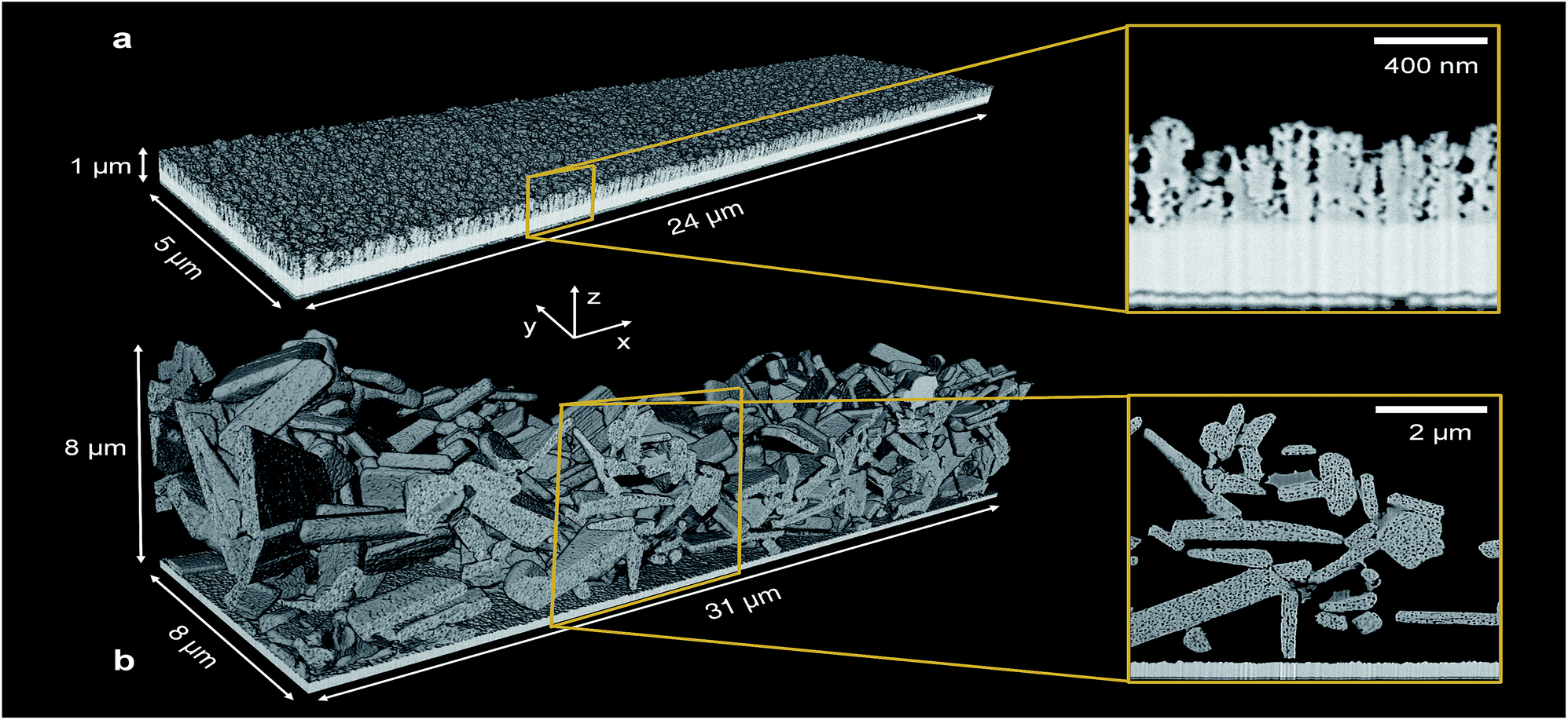 | ||
| Fig. 1 3D rendering of (a) the hematite photoelectrode with a 4 × 4 × 4 nm3 voxel volume size and a recorded volume of 1 × 5 × 24 μm3, and (b) the LTON photoelectrode with a 8 × 8 × 8 nm3 voxel volume size and a recorded volume of 8 × 8 × 31 μm3. For both samples, a detailed view of the first SEM image of the acquired stack is shown. | ||
3. Photoelectrode characterization
3.1 Macroscopic structural characterization of photoelectrode films
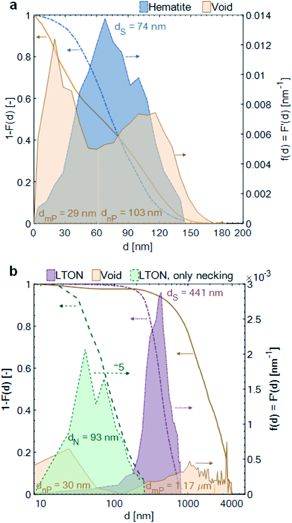 | ||
| Fig. 2 Cumulative opening size distribution (left y-axis) and probability opening size distribution (right y-axis) of the semiconductor films. (a) Hematite semiconducting phase (blue) and pore space (yellow). (b) LTON semiconducting phase with necking (violet), pore space (yellow), and TiO2 necking phase only (green). The TiO2 probability opening size distribution has been scaled down by a factor of 5. | ||
The pore space, filled with electrolyte in the operating PEC electrode (as long as the pore network is percolating and the capillary pressure is high enough for the electrolyte to penetrate into the smallest pores), had a mean diameter between hematite branches of 29 nm [dmin = 0 nm, dmax = 60 nm]. The mean diameter of the pore space, due to inhomogeneity of film thickness, i.e. between the thinnest and thickest film region, was 103 nm [dmin = 60 nm, dmax = 185 nm]. The pore space of the LTON film was divided into three different length scales: the nano-pores (nP) within individual LTON particles, having a mean diameter of 30 nm [dmin = 0 nm, dmax = 128 nm], the meso-pores (mP) between the individual LTON particles, having a mean diameter of 1.17 μm [dmin = 128 nm, dmax = 2 μm], and the mean characteristic diameter of the pore volume developing between the thickest and thinnest region of the film, having a mean diameter of 3.03 μm [dmin = 2 μm, dmax = 4 μm].
The opening size distribution of the necking phase (TiO2) in the LTON electrode revealed that the average diameter of the necking was 93 nm [dmin = 0 nm, dmax = 256 nm]. Together with the results from the volume fraction profile, these small sizes of the necking patches indicate that, apart from the first layer of LTON particles (well connected to the FTO), the charge generated in particles higher up in the film must be transported through multiple TiO2 necking patches, and particles before reaching the FTO substrate.
3.2 Feature characterization on multiple scales
As applied to the LTON photoelectrode, the dimensions, shapes, and orientations of the individual LTON particles (micrometer scale) and the nano-pores (pores within the hosting LTON particle in nanometer scale) were quantified. For the particle analysis, individual particles had to be identified within the interconnected particle network. For the nano-pore analysis, the individual nano-pores had to be assigned to the hosting particles. However, a proper segmentation of the particles posed difficulties due to the plate-like shapes of the particles, high aspect ratios, and locally dense stacking. For this purpose, we developed an algorithm to fit ellipsoids, grown from manually placed seed points, into the dataset (see Methods). Prior to this process, the nano-pores were artificially eliminated with a low pass filter. In Fig. S7,† the computed ellipsoids are visualized in the LTON geometry.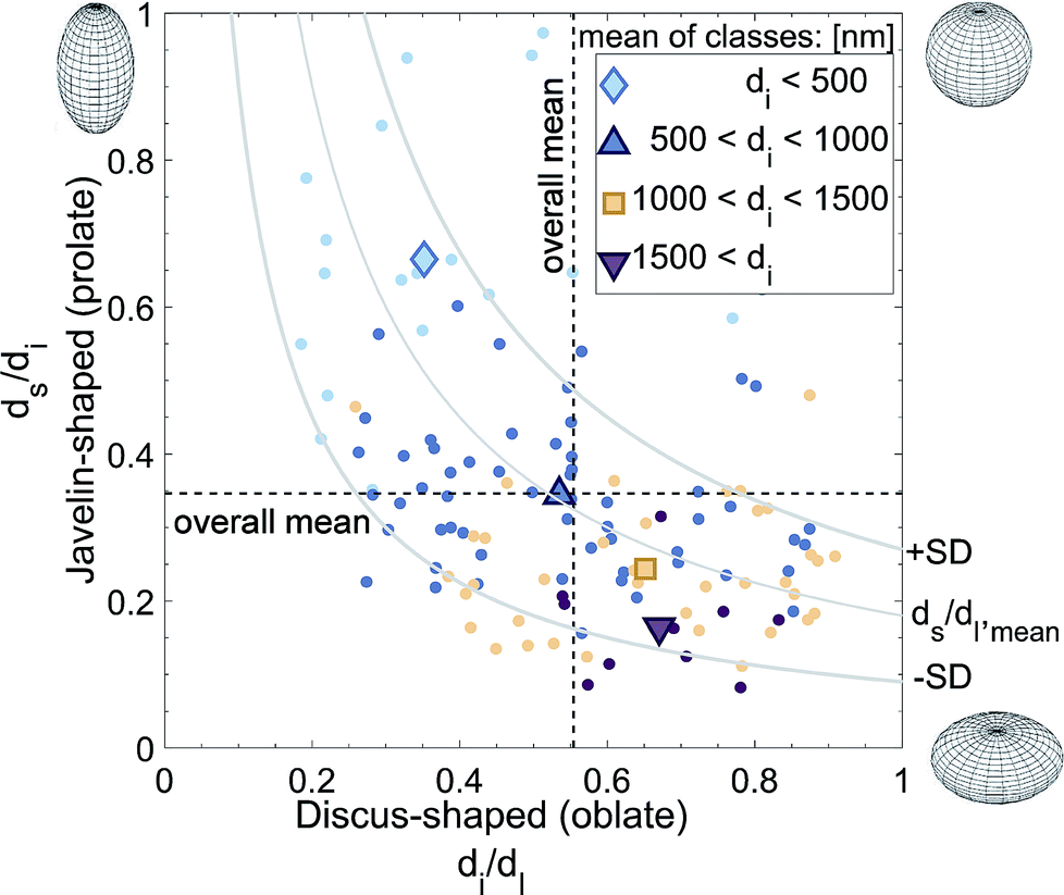 | ||
| Fig. 3 Shape analysis of the computed ellipsoids. The ellipsoids are divided into 4 classes based on the length of the intermediate diameter. The mean value shifts from prolate to oblate shapes for classes with larger di. Overall, the ratio ds/dl stays constant. Isolines for ds/dl are shown for the mean = 0.18 ± SD. | ||
Based on the ellipsoid fitting, the particle volume distribution was estimated by assuming cubically shaped particles (Fig. S9†). In this case, the volume of the particles can be approximated by the volume of the box surrounding the ellipsoid. The lognormal distribution function had a mean of 0.521 μm3, a standard deviation of 0.544 μm3, and a median of 0.338 μm3.
Quantifying the bounding boxes allows the estimation of the areas of specific surface plane types known to be implicated in photoelectrode performance. Pokrant et al.12 correlated specific crystallographic planes with LTON particle faces and found that the biggest surface corresponds to the (100) plane, the medium surface to the (001) plane and the smallest surface to the (010) plane. Following this model, we quantified the ratio of these surface types. In an ideal case with non-touching particles, the (100) plane accounted for up to 70.57% of the overall outer particle surface, the (001) 19.33%, and the (010) 10.10%. If one knows the activity of the surface plane types, for example by ab initio calculations, then the results here are key to estimating the performance potential of LTON particles and electrodes.
Using the eigenvectors of the ellipsoid radii, the orientation of the particles with respect to the FTO substrate was determined (Fig. S10†). Due to their plate-like nature, the orientation of the particles was quantified using the smallest diameter axis (standing normal on the largest particle surface). The smallest diameter vector is perpendicular to the electrode plane for a particle lying flat on the FTO, and an elevation angle of 90° was assigned. The elevation angle was set to 0° for a particle standing on an edge (i.e. the smallest diameter vector is parallel to the FTO substrate). No trend of particle orientation as a function of the z-positon in the film was found. Only a small percentage of particles laid flat or almost flat in the film. For the most part, the normal vectors of the particles were elevated by 10° or 45°. This is a desirable result, as the incoming light is absorbed along the long axes of the particles, the minority carriers have a short way to the electrolyte, and the majority carriers have to pass through fewer TiO2 necking patches.
The nano-pore orientations relative to the orientation of the hosting particle were also quantified. The semi-axes of the ellipsoid were used as the reference coordinate system (Fig. 4a). An azimuth and an elevation angle of 0° corresponded to an elongated pore directed along the x-axis, the direction of the longest particle diameter dl. The calculated pore orientations were translated into crystallographic directions based on an orthorhombic LTON unit-cell with unit-cell parameters: a = 5.57137 Å ([100]), b = 7.8790 Å ([010]), and c = 5.60279 ([001]).13Fig. 4b shows the 2D histogram of the relative nano-pore orientations based on all pores in 4 particles with a volume greater than 30 voxels. The volume threshold filtered out small pores for which the algorithm was not able to determine the orientation. The frequency of the elevation angles was normally distributed around 0°. Considering only the elevation angles between 0° and 5°, an overall maximum in the azimuth angle distribution was found at −30° and the corresponding local maximum at 150° was shifted by +180°. A high number of pores was elongated in the [010] direction, which corresponds to the longest semi-axis of the particle. However, the 2D histogram revealed that the pore orientations along the [011] direction belong to the most frequent elongation direction. With this result we quantitatively confirmed the qualitative TEM-based hypothesis12 that the nano-pore elongation direction follows a major crystal axis (Fig. S11†). We also proved that we are able to analyze complex 3D porous networks utilizing FIB-SEM tomography with a higher resolution than 10 nm.
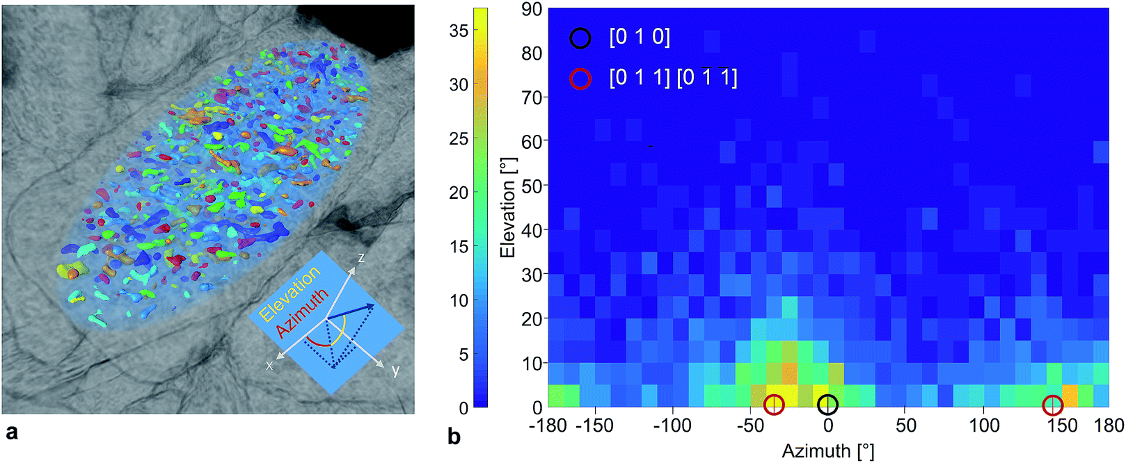 | ||
| Fig. 4 (a) Rendering of an ellipsoid (blue) fitted into a LTON particle, and of nano-pores within the ellipsoid. The semi-axes correspond to crystallography directions of x = [010], y = [001], and z = [100]. An azimuth and an elevation angle of 0° corresponds to the direction of the x-axis. The pores in the network were separated using watershedding and visualized with individual colors. (b) 2D histogram of the nano-pore orientations in 4 different LTON particles relative to the orientation of the hosting particle. Three crystallography directions are indicated. The nano-pores are most frequently elongated in the [011] direction. | ||
3.3 Transport characterization by direct pore-level simulations
The measured absorption coefficient showed a weak wavelength dependency between 300 nm and 590 nm (bandgap). Therefore, the generation rate profile was calculated for a constant wavelength-averaged absorption coefficient of 1.4 × 104 cm−1. The mean deviation from the exact profile was 1.1% and 1.6%, for front and back illumination respectively. Based on this finding, the generation rate profiles and the local current densities were calculated for constant absorption coefficients ranging from 5 × 10³ to 1 × 105 cm−1 and a constant bandgap of 2.1 eV. The results showed that the influence of the morphology on the generation rate profile increases with higher absorption coefficients. For an absorption coefficient of only 5 × 104 cm−1, the shape of the generation rate profile is already dictated by the volume fraction profile. A maximum absorbance of 97.3%, equivalent to a maximum current of 9.5 mA cm−2 (per flat photoelectrode area), can be reached with a high absorption coefficient of 1 × 105 cm−1; the remaining part is always lost due to small areas not covered by any particle. For all absorption coefficients, the maximum current density for front illumination was 9–13% lower than for back illumination. Also, for low absorption coefficients (<8 × 103 cm−1), evenly distributed current densities with low values (<4 mA cm−2) were found, which is desirable in order to avoid degradation. High absorption coefficients (>5 × 104 cm−1) resulted in big fractions of the surface area having high current densities, up to 11 mA cm−2.
| ALCC = acie(−bci) ≤ 1 | (1) |
| a = Φ>EgAnD(a1/α2 + a2) [m3 mol−1] | (2) |
| b = Φ>EgAnD(b1/α2 + b2) [m3 mol−1] | (3) |
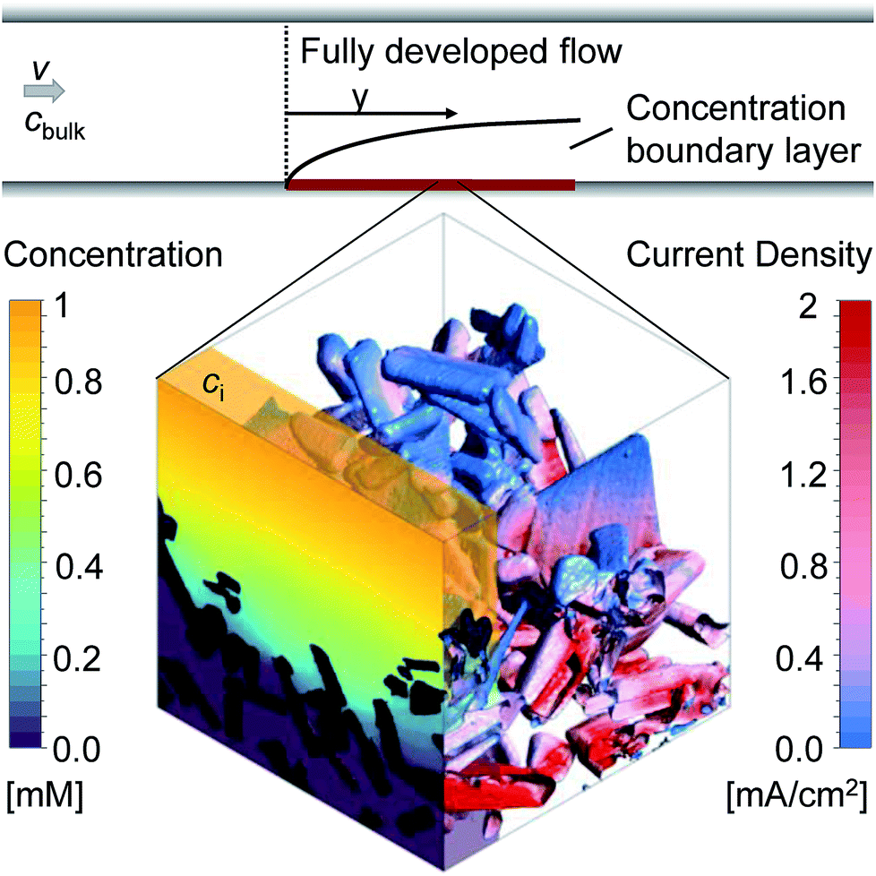 | ||
| Fig. 5 Example of calculated current densities for back illumination (α = 1.4 × 104 cm−1) and OH− concentrations (ci = 1 mM). The electrolyte is stagnant in the pore space and by a Sherwood correlation, the contributions of the hydrodynamic boundary layer in a flow cell setup is taken into account. | ||
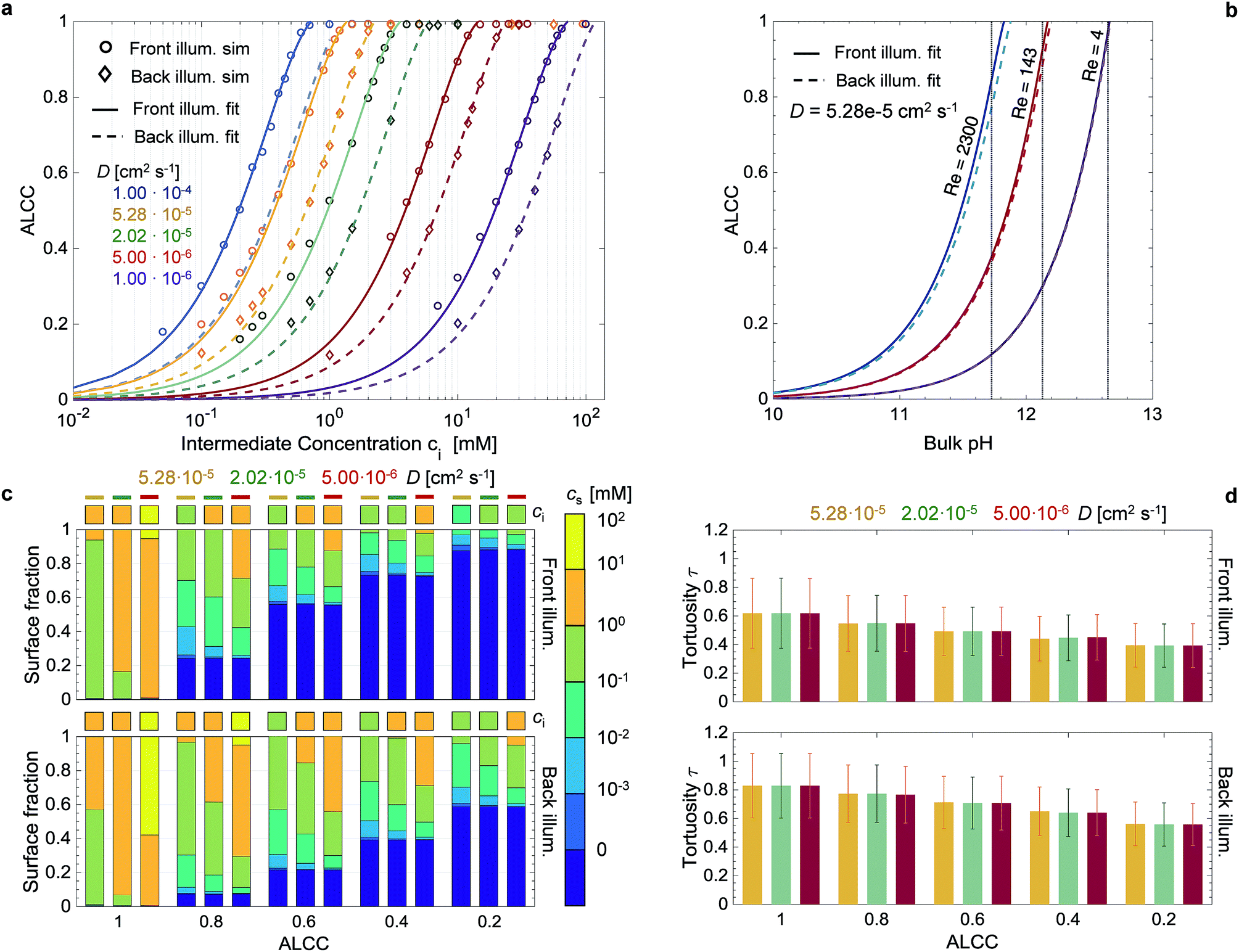 | ||
| Fig. 6 (a) Simulated values and fit for the absorbed-light-to-charge-transfer-conversion (ALCC) as a function of the intermediate concentration and the diffusion coefficient. (b) The ALCC correlated to the bulk pH for different flow regimes of a flow cell water splitting device with NaOH as an electrolyte. (c, d) The surface concentration distributions, cs, at the semiconductor–electrolyte interface and the tortuosity, τ, at different ALCC values for 3 diffusion coefficients for front and back illumination. (c) The histogram bars are binned with a logarithmic scale and the square above the bar indicates the intermediate concentration ci corresponding to the ALCC. (d) The tortuosity corresponds to the mean path length of the reactants divided by the film thickness. The error bars indicate the standard deviations of the normal distributed tortuosity. | ||
Both a and b are linearly dependent on: the integral of the incoming photon flux (with energies above the bandgap), Φ>Eg [m−2 s−1], the absorbance, A [—], the number of charges transferred at the semiconductor–electrolyte interface per reactant, n [—], and the diffusion coefficient of the reactant in the fluid phase, D [m2 s−1]. Finally, there is an inverse quadratic dependency of a and b on the absorption coefficient α [m−1]. The first two parameters define the maximum possible current per irradiated flat area, and the multiplication with n defines the maximum possible reactant flux through a plane perpendicular to the irradiation direction. Any increase in this overall flux shifts the curve of the ALCC to higher ci, and a decrease shifts it to lower ci. In Fig. 6a, the linear dependency between the diffusion coefficient and the parameters a and b has been demonstrated by fitting a = a0D and b = b0D in eqn (1) to all the simulated data points (same absorption coefficient), with a RMS = 0.014 for front illumination and a RMS = 0.016 for back illumination. As shown in Fig. S16,† the ALCC highly depends on the generation rate profile, or more specifically, the absorption coefficient and the volume fraction profile. For front and back illumination, the results showed a shift to higher ci for larger absorption coefficients. For the front illumination, this was mainly due to the increased generation rate. For the back illumination, the shift to higher ci is much more pronounced, as a larger absorption coefficient also shifts the generated charges to lower positions in the film, thus making it more difficult for the reactants to reach. In both cases, the ALCC curves asymptotically merged with high absorption coefficients. As previously discussed, in this range of high absorption coefficients, the generation rate profile is purely dependent on morphology, and thus constant. This behavior can be described by an inverse quadratic dependency with the fitting parameters a1, a2, b1, b2. The parameters a1 and b1 are weights to control the decrease of a and b with increasing absorption coefficients. The parameters a2 and b2 characterize the effect of morphology on the ALCC. Eqn (1) to (3) were fitted to the data points in Fig. S16,† respecting the previous fit for a0 and b0. For front illumination, the parameters a1 = 2.254 × 10⁻¹, a2 = 4.714 × 10⁻¹³, b1 = 8.217 × 10⁻², and b2 = 1.709 × 10⁻¹³ were calculated with RMS = 0.032. For back illumination, the parameters a1 = 2.538 × 10⁻¹, a2 = 2.003 × 10⁻¹³, b1 = 9.536 × 10⁻², and b2 = 6.871 × 10⁻¹⁴ were calculated with RMS = 0.041. The parameters a2 and b2 are more than two times smaller for back illumination than for front illumination, which confirms them as morphology-descriptive parameters. Smaller parameters a2 and b2 lead to a shift of the ALCC to higher ci. The morphology has a much stronger effect on the ALCC for the back illumination case, as the generation rates are much deeper in the film, and mass transport limitations occur at higher concentrations.
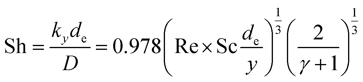
The correlation found between ci and ALCC can be combined with a macroscopic Sherwood correlation, describing the hydrodynamic boundary layer, to link the ALCC to a bulk concentration, cbulk. To quantify a realistic hydrodynamic boundary layer, the LTON photoelectrode was considered to be in a PEC flow cell,14 and the transport of OH− ions into the pore space of the LTON electrode for the oxygen evolution reaction in a water splitting device was studied (Fig. 5). For the specific case of a flow cell, the Sherwood correlation described in the Methods was used. However, eqn (1) can be linked to any other appropriate correlation in another reactor setup. The ALCC as a function of the bulk pH of an aqueous NaOH solution is shown in Fig. 6b for 3 different flow regimes: almost stagnant, Re = 4; medium velocity, Re = 143; and maximum velocity in laminar flow, Re = 2300. The bulk pH for which the mass transport through the macroscopic concentration boundary layer begins to be limiting is indicated with a dotted line. For Re = 4, the macroscopic mass transport limit was predicted to begin below a bulk pH of 12.6. The microscopic LTON structure had a minimal effect in this flow regime, and the illumination direction did not play a role. For Re = 143 and Re = 2300, the mass transport limitation was due to LTON morphology, and the difference between front and back illumination was more pronounced for higher Re. For the given case, mass limitations occurred only for relatively low bulk pH values (bulk pH < 12.6, Re = 4), and in a flow cell setup, those mass transport limitations were shown to be effectively reduced by increasing the velocity (bulk pH < 11.82, Re = 2300). However, with our multi-scale correlation, we not only predict the bulk pH below which the mass transport is limited, but also describe the ALCC as a function of the bulk pH. In addition, the local surface concentrations, cs, along the semiconductor–electrolyte interface are quantified for different diffusion coefficients at specific ALCC values. Fig. 6c shows the results for D = 5.28 × 10⁻⁵ cm2 s−1, D = 2.02 × 10⁻⁵ cm2 s−1, and D = 5.00 × 10⁻⁶ cm2 s−1 at ALCC = 1, 0.8, 0.6, 0.4, and 0.2. The concentration distribution is analyzed by using histogram bins in the logarithmic scale. The surface fractions for surfaces with zero concentration are, by definition, identical for all three diffusion coefficients at a given ALCC. For decreasing ALCC values, the surface fraction of surfaces in depleted electrolyte regions increases. For both illumination directions, the depletion of the electrolyte began in regions above the FTO, which are the furthest from the bulk concentration. In the case of front illumination, a sharp increase of surfaces with zero concentration was observed from ALCC = 1 to 0.6. The charges are generated high up in the film, and almost 60% of the surfaces were depleted for a 40% decrease of the overall mass flux. The rate of surface depletion diminished afterwards for lower ALCC values. For back illumination, the surface fraction of depleted surfaces was always much lower compared to front illumination for the same ALCC. For back illumination, the peak of the generation rate was confined to the bottom of the LTON film and the ALCC was influenced by the first surface areas that were depleted. Also, the surface fraction of depleted surfaces increased linearly with decreasing ALCC. In Fig. 6c, the order of magnitude of the intermediate concentration for each ALCC and diffusion coefficient is indicated above each histogram bar. For ALCC = 1, the calculated surface concentrations were, at most, one order of magnitude smaller than the intermediate concentrations, resulting in small concentration gradients throughout the pore space of the structure. This quickly changed for ALCC = 0.8, where a wide distribution of surface concentrations was observed. The magnitude of the diffusion coefficient determined the surface fraction at each concentration. Larger diffusion coefficients resulted in a broader concentration distribution along the film thickness, and low surface concentrations (10−3 to 10−1 mol m−3) had a higher surface fraction. The concentration gradient was much higher for low diffusion coefficients, and most of the surface concentrations were closer to the intermediate concentration for a given ALCC. This was observed for front and back illumination. In general, the computed results provide unique insight into the influence of morphology on local surface concentration distributions. The data can be used to study the degradation of structured semiconductor electrodes due to locally quantified pH values in which the semiconductor is not stable. The specific case of the LTON photoelectrode in aqueous NaOH electrolyte was analyzed and the surface fractions of local pH values vs. bulk pH values are shown in Fig. S17.† The ALCC was below 1 for bulk pH values smaller than 12.6 and Re = 4. For higher bulk pH values, the local pH on the electrolyte–semiconductor interface was not affected by the morphology. However, for smaller bulk pH values, e.g. 12.5, local pH values (down to pH 7) were found. For LTON, which is stable only at high pH values (above 13), we never reached a condition where morphology would locally reduce the pH and degrade the semiconductor. The introduced approach could also be applied to an electrode for CO2 reduction, where local pH gradients are also desired to promote the activity of a catalyst towards the production of a specific product.
The tortuosity was calculated for the same conditions as the surface concentration calculations and is shown for front and back illumination in Fig. 6d. The tortuosity was defined as the mean path length of the reactants travelling from the intermediate concentration plane to the semiconductor surface divided by the LTON film thickness. Therefore, the tortuosity can be smaller than 1, as most reactants do not travel through the whole film thickness (Fig. S18†). The path lengths were normal distributed and the error bars indicate the standard deviations. The tortuosity was generally larger for back illumination, as the key parameter is the generation rate profile calculated from the light absorption (Fig. S13†). For both illumination directions, the tortuosity decreased for smaller ALCC values due to the creation and growth of the depletion regions. For a given ALCC value, the influence of the diffusion coefficient was negligible. Despite the complex structure of the LTON film, the mean values of the path lengths did not exceed the film thickness, even in the case of no mass transport limitations.
4. Conclusions
For the first time reported, we have successfully used nano-tomography to acquire the detailed geometries of morphologically-complex PEC electrodes. This data was digitalized and used to provide a quantitative analysis of the structure of two morphologically-complex photoelectrodes: a particle-based lanthanum titanium oxynitride electrode with a film thickness of a few micrometers, and a ‘cauliflower-like’ structured hematite electrode with a film thickness of a few hundred nanometers. We used a combined experimental-numerical approach in which we obtained the exact structural information by destructive, ex situ FIB-SEM tomography and digitalized the structure utilizing advanced post-processing and segmentation algorithms. We then used various computational algorithms to quantify the morphological properties on multiple scales: (i) the solid phase material distribution along the electrode thickness, specific surface, mean feature dimensions, and film homogeneity on the macro-scale; (ii) particle shapes, surfaces, volumes, and orientations on the meso-scale; and (iii) nano-pore volumes and orientations on the nano-scale.Detailed semiconductor material distribution profiles along the electrode thickness were obtained and provide relevant information for light absorption. Surface characterizations on the exact geometry allowed decoupling of contributions from the meso-scale features and the nano-scale pores, suggesting that the connected nano-pore surfaces represent 31% of the overall surface. Advanced segmentation of the tomography data, based on machine learning algorithms which can distinguish different grey value patterns, led to the identification of the TiO2 necking phase in the LTON electrode and revealed that necking spans short distances between particles only. These results prove that majority carriers must be transported through multiple particles and necking patches in order to reach the FTO back-contact. An algorithm was developed which performs ellipsoid fitting into the particle-based LTON structure. This algorithm allows for the identification and characterization of individual particles in the highly interconnected particle network. Quantitative characterization of single LTON particles was then obtained by calculating frequency distributions of particle diameters and volumes, as well as particle shapes and orientations. The surface area of the particles was calculated and contributions from the characteristic particle facets, which are linked to crystallographic planes, were estimated. The high resolution of the FIB-SEM tomography gave quantitative insight into the nano-pore volumes within the LTON particles and allowed determination of the crystallographic directions, to which the pores were preferentially elongated.
Multi-physical transport characterizations were performed on the LTON photoelectrode using direct pore-level simulations. The exact 3D morphological geometry was used to investigate light absorption in the semiconductor and mass transport through the liquid space of the LTON particle network. Current densities for front and back illumination were calculated and imposed as a boundary condition at the semiconductor–electrolyte interface. The influence of the absorption coefficient on the generation rate profile was analyzed and resulting current density distributions were quantified. The mass transport calculations were done on multiple scales, simulating the purely diffusive transport of reactants through the stagnant pore space and correcting the result with a Sherwood correlation to take into account the concentration gradients in the macroscopic hydrodynamic boundary layer. The mass transport induced performance drop of the photoelectrode was described as a function of the semiconductor and electrolyte properties, the incident radiation, and ultimately linked to the morphology. Local concentration distributions on the semiconductor–electrolyte interface were quantified for various ALCC values and diffusion coefficients. For the same conditions, the tortuosity of the reactants within the LTON film was calculated.
This study presents the first in-depth geometrical quantification and multi-physical transport characterization of morphologically-complex photoelectrodes. The data acquisition with the FIB-SEM nano-tomography provides the detailed morphology-information to study the film structure, characterize the individual building blocks on multiple scales, and to run pore-level transport simulations on a representative volume. The method we developed contributes to guiding the morphology and fabrication of optimized photoelectrodes with enhanced performance.
5. Methods
5.1 Sample preparation
For FIB-SEM tomography, the FTO with the deposited films were embedded in epoxy. The effect of the epoxy is to provide mechanical support for free standing structures, obscure the off-section features, in addition to increasing contrast of the SEM image. The epoxy embedding medium was diluted with acetone at a ratio of 1![[thin space (1/6-em)]](https://www.rsc.org/images/entities/char_2009.gif) :3 and the electrode was dip coated and put in a vacuum for 20 min. This step was repeated twice at an epoxy/acetone ratio of 2:2 and 3:1. The sample was then dip coated in a pure resin, put in a vacuum for 20 min, and then polymerized for 24 h at 60 °C. Subsequently, a wedge was polished with a tripod polishing tool using diamond lapping film discs of 6 μm, 3 μm, 1 μm, 0.5 μm roughness. The polishing was necessary to decrease epoxy thickness to a few hundred nanometers above the volume of interest. A thin film of gold was sputtered onto the epoxy to diminish the charging effect during electron beam imaging. A fiducial platinum film was deposited in the FIB-SEM over the region of interest. V-shaped alignment reference marks were milled into this film and covered by a 1 micron thick carbon layer to increase the contrast.
:3 and the electrode was dip coated and put in a vacuum for 20 min. This step was repeated twice at an epoxy/acetone ratio of 2:2 and 3:1. The sample was then dip coated in a pure resin, put in a vacuum for 20 min, and then polymerized for 24 h at 60 °C. Subsequently, a wedge was polished with a tripod polishing tool using diamond lapping film discs of 6 μm, 3 μm, 1 μm, 0.5 μm roughness. The polishing was necessary to decrease epoxy thickness to a few hundred nanometers above the volume of interest. A thin film of gold was sputtered onto the epoxy to diminish the charging effect during electron beam imaging. A fiducial platinum film was deposited in the FIB-SEM over the region of interest. V-shaped alignment reference marks were milled into this film and covered by a 1 micron thick carbon layer to increase the contrast.
5.2 Ion beam milling and image acquisition
We used a Zeiss NVision 40 Crossbeam system for the FIB-SEM tomography. The sample was mounted on the sample holder and tilted by 52° to align the ion beam column perpendicular to the sample surface. The ion beam was used to erode a trench in front of the volume of interest, allowing for accessibility and the acquisition of a first cross-section image by the scanning electron beam. Automated drift-correction and beam tuning (focus and stigmator) was needed in order to acquire a stable sectioning of the sample for hundreds of images and to maintain spacing between the images in accord with SEM resolution (4 nm). The Atlas3D system (Fibics, Inc.), a scan generator and image acquisition system of Zeiss devices, can cope with various drift phenomena (electron beam and ion beam), as well as a shift in imaging conditions, by assessing the position of the reference marks in the platinum layer. FIB milling and SEM imaging were done simultaneously to reduce overhead time. The ion beam continued to mill while the electron beam returned to start the scan of a new line (“fly-back”), and blanked when the electron beam acquired a line of the image in order to eliminate interference in the secondary electron images.15 FIB milling was done at an acceleration voltage of 30 kV and a 300 pA beam current, and the SEM images were recorded with an acceleration voltage of 1.7 kV and 1 nA. We ran the FIB-SEM tomography for 24 h to obtain at least 1000 consecutive images of stable cross-sections. Secondary electron (SE) and backscattered electron (BSE) signals were recorded simultaneously.5.3 Digital reconstruction
The data for the hematite electrode was acquired with an isotropic voxel size of 4 × 4 × 4 nm3 and consisted of 1354 images with the dimension of 6204 × 1000 pixels. The LTON electrode was measured with an isotropic voxel size of 8 × 8 × 8 nm3, giving 1000 images with the dimension of 4065 × 1400 pixels. All the image post-processing in the following discussion used the images from the SE signal and was implemented in the open-source tool Fiji.16Image Registration—despite the 3D tracking during data acquisition, translational drift occurred. This remaining drift was corrected by a registration process utilizing three notches milled into the platinum layer along the sectioning direction as alignment marks. The mark on the first image was used as a template and matched by a normalized correlation coefficient matching method to the following marks to determine the image translation and to align the slices using the plug-in Template Matching.17 In the case of the relatively thick LTON sample, the images were inconsistently compressed in the height of the image due to charging effects that can deflect the electron beam. This compression was compensated for by aligning the bottom of the FTO throughout the stack and by expanding or compressing the individual images accordingly. Typical compression factors were in the range of 4 to 10 voxels.
Filtering and 3D rendering—a major challenge was the removal of air bubble artifacts in the images. These bubbles formed in the epoxy during the sample preparation. In Fig. S1a,† the bubbles can be seen on the surface of the LTON particles, or in narrow gaps between the particles. A low pass filter was applied in the frequency domain, derived by a discrete Fourier transformation, to blur the pores in the particles. A histogram-based threshold segmentation and a stack erosion step, with a structuring disk of 5 pixels in diameter, was applied on the filtered images. After the erosion of the solid phase, the artifacts were disconnected from the solid phase and, by selecting only the larger connected solid volumes, a binary mask was obtained to remove the signal from the bubbles in the SEM images.
Segmentation—we used a grey value histogram-based segmentation in order to differentiate between the solid and void domains and eventually digitalize the reconstructed dataset of grey values. A coarse segmentation of the structure for the two introduced photoelectrodes was straightforward, as the epoxy in the void domain had a high carbon level with a big electron beam interaction volume leading to a low signal to noise ratio. The fine tuning of the segmentation, however, highly depended on the quality and contrast of the acquired SEM images and needed to be adjusted for each dataset individually. For sample (i), the smallest hematite features had a diameter of a few nanometers and suffered from edge effects. Edge effects appear when the scanning electron beam hits a small feature. Secondary electrons leave the feature through all surrounding edges, resulting in an increased brightness, but a less sharp solid–void interface. We used an 8 bit threshold of 125 for the segmentation. This threshold lied symmetrically between the two extreme thresholds of 100, where all grey values except the background were included, and 150, where small features started to disconnect from the main solid phase.
For sample (ii), the outer interfaces between the LTON particles and void were well defined and sharp. However, the inner pores were not properly filled with epoxy and showed weak contrast. The necking phase between the particles could be visually distinguished from the LTON by the texture and contrast in the electron beam image, and was segmented by a machine-learning algorithm trained on manually selected image features using the Trainable WEKA Segmentation plug-in.18 Before applying the plug-in, the contrast was improved by contrast limited adaptive histogram equalization19 using the Enhance Local Contrast (CLAHE) plug-in in Fiji. The quality of the segmentation could only be assessed visually and is shown in Fig. S1b.† Fig. S1c† shows the 3D rendering of the TiO2 necking. An animated version is available in ESI.† The individual TiO2 phases were labeled and connected TiO2 phases were given the same color. For the first time, the TiO2 necking was visualized and quantified, and its ability to connect the LTON particles, ideally over a length scale of multiple particles, was assessed. Once the TiO2 phase is subtracted, the LTON was segmented with an 8 bit threshold value of 92. An upper threshold of 106, where all the nano-pores were connected, and a lower threshold of 78, where only volumes entirely filled by epoxy were considered to be pores, were used to define error bars on the results, i.e. the sensitivity of the obtained results on the threshold accuracy.
5.4 Volume fraction profile
The volume fractions of the solid components as a profile throughout the photoelectrode film along the z-axis was computed using a voxel-based approach. The volume of each pixel was assigned to a component based on the grey value and the threshold. The solid volume fraction of each pixel layer parallel to the substrate plane was determined by the ratio of the number of pixels of a component and the total number of pixels in that layer. The volume fraction profile was drawn perpendicular to the FTO surface, which was set as the origin (z = 0).5.5 Surface area
The surface area was calculated by creating a triangular surface mesh and integrating over all triangle areas. The surface mesh was generated using the marching cube algorithm.20 Eight neighboring voxels forming the corners of a cube defined the surface polygon that divided the cube into the solid and void phases. The scalars of the grey values determined the intersection points with the cube edges. The algorithm marched through the dataset and neglected the surface triangles touching the boundaries of the scanned volume.5.6 Size distributions
The feature size at any point in the solid phase of the photoelectrode geometry was characterized by the biggest sphere that fits into the structure.21 This was calculated by applying mathematical morphology operations. After a threshold segmentation, the binary dataset was sequentially processed by an opening algorithm with a structuring element, increasing in size. The opening algorithm consisted of a 3D morphological erosion, followed by a 3D morphological dilation, using a sphere with a diameter d,22 and thus, eliminated all features smaller than the structuring element. The cumulative opening size distribution 1 − F(d) = ε(d)/ε0 was determined by calculating the porosity, ε, after each step and relating it to the initial porosity, ε0. Its derivation lead to the size distribution, f(d) = F′(d). The mean diameter is given as: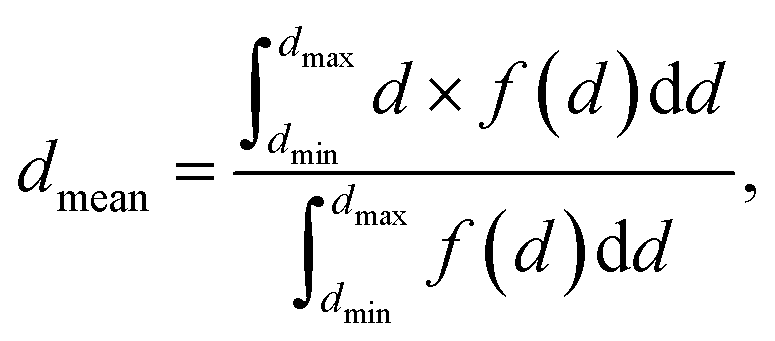 | (4) |
5.7 Particle properties
An algorithm to fit ellipsoids into individual particles of an interconnected particle network was developed. The algorithm was only relevant for sample (ii) and was based on the principle of finding the maximal inscribing ellipsoid, for a given seed point, into a binary dataset. We used the matrix definition of an ellipsoid,| (X − X0)TH(X − X0) ≤ 1, | (5) |
5.8 Nano-pore characterization
For sample (ii), the nano-pores within single LTON particles were characterized. The inner porosity, as the volume fraction of the pores within the particles, was computed using a voxel-based approach. Only the voxels that were located within the previously calculated ellipsoid volumes were extracted and segmented with a threshold value of 92. The inner porosity was calculated for each ellipsoid and then averaged. The connectivity of the nano-pore space was assessed by a 3D flood fill algorithm25 starting from the inter-particle void space and subsequently flooding all the connected void phase voxels. The orientations of the pores relative to the orientation of the hosting ellipsoid were characterized. The pores within a given ellipsoid were separated by water shedding in order to break the pore network down into single, non-diverging volumes. The main elongations of these pores were computed by the tensors of inertia in Avizo, giving the orientations of the longest semi-axis of an ellipsoid fitted into each pore volume.5.9 Generation rate and local current density
The spectral reflectance, ρm, and the transmittance, τm, were acquired with a UV-3600 Shimadzu UV-VIS-NIR spectrophotometer using an integrating sphere. The sample was illuminated from the FTO-side and therefore, ρm has to be corrected by the absorbance of the FTO glass: ρc = ρm + αFTO. The transmittance and the reflectance of the FTO glass were measured separately and the absorbance was calculated by: αFTO = 1 − ρFTO − τFTO. The effective absorption coefficient is determined using a single partially transmitting layer with a thickness greater than the wavelength, considering multiple internal reflections: | (6) |
 where V(z) is the averaged volume fraction profile along the z-direction given in Fig. S2.†
For the calculation of the generation rate, a subsample of the segmented FIB-SEM data set was discretized in all three directions. For constant x = i, y = j and z = k values, the generation rate per solid volume, Gi,j,k was calculated as:
 | (7) |
 | (8) |
 | (9) |
| ∇(D∇c) + Sc = 0 | (10) |
5.10 Mass transport
Mass transport of reactants within the void phase of the complex morphology was modeled as diffusion in a stagnant fluid. For the assumptions of zero fluid velocities and infinitely diluted species, diffusive transport equation was solved until steady state was reached: | (11) |
The void phase of the FIB-SEM dataset was meshed using a tetrahedral mesh generator26 and the diffusive transport equation was solved with a commercial finite volume solver.27 A schematic of the simulation setup is show in Fig. S15.† An intermediate concentration ci was set as a top boundary condition. The side walls had symmetry boundary conditions and the bottom, which was covered by FTO had a no-flux boundary condition. The calculated local current density was applied as a reactant sink boundary condition onto the electrolyte–semiconductor interface. The boundary flux was given as a step function, being the charge flux calculated by the generation rate for a boundary concentration cBoundary > 0, and being 0 for cBoundary = 0. It was assumed that the photo-induced potential drop occurs only in the space-charge layer of the semiconductor and in the Helmholtz layer,28 thus, ions are not driven by an electric field, but only travel by diffusion. This assumption is correct for ionic concentrations in the electrolyte with a small Debye length. For our calculations, the ionic strength in most parts of the domain is high enough to keep the Debye length below 1 nm; however, for the domain regions with near depletion, the Debye length increases and contributions from the electric field through migration were neglected. The mass transport through the macroscopic hydrodynamic boundary layer in a laminar-flow parallel plate cell was taken into account by the experimentally determined Leveque-correlation:29
 | (12) |
The tortuosity was calculated with the mean path lengths of the reactants divided by the film thickness. 2500 pathlengths were extracted from the derivative of the reactant concentration field. The start points of the pathlengths were uniformly distributed on the plane of the intermediate concentration ci.
Conflicts of interest
There are no conflicts to declare.Acknowledgements
This material is based upon work performed with the financial support of the starting grant of the Swiss National Science Foundation, as part of the SCOUTS project (grant #155876), and of the Hans-Eggenberger Foundation. We thank Matt Mayer, EPFL, for providing hematite samples. We thank Danièle Laub, EPFL, for the tomography sample preparation.References
- H. R. Kim, G. Kim, S. Il In and Y. Park, Optimization of porous BiVO4 photoanode from electrodeposited Bi electrode: Structural factors affecting photoelectrochemical performance, Electrochim. Acta, 2016, 189, 252–258 CrossRef CAS.
- O. K. Varghese, M. Paulose and C. A. Grimes, Long vertically aligned titania nanotubes on transparent conducting oxide for highly efficient solar cells, Nat. Nanotechnol., 2009, 4(9), 592–597 CrossRef CAS PubMed.
- M. T. Mayer, C. Du and D. Wang, Hematite/Si nanowire dual-absorber system for photoelectrochemical water splitting at low applied potentials, J. Am. Chem. Soc., 2012, 134(30), 12406–12409 CrossRef CAS PubMed.
- Y. Qiu, et al., Efficient photoelectrochemical water splitting with ultrathin films of hematite on three-dimensional nanophotonic structures, Nano Lett., 2014, 14(4), 2123–2129 CrossRef CAS PubMed.
- J. Li, et al., Si nanopillar array optimization on Si thin films for solar energy harvesting, Appl. Phys. Lett., 2009, 95(3), 33102 CrossRef.
- Z. Zhang and P. Wang, Optimization of photoelectrochemical water splitting performance on hierarchical TiO2 nanotube arrays, Energy Environ. Sci., 2012, 5(4), 6506 RSC.
- A. Kay, I. Cesar and M. Grätzel, New benchmark for water photooxidation by nanostructured alpha-Fe2O3 films, J. Am. Chem. Soc., 2006, 128(49), 15714–15721 CrossRef CAS PubMed.
- S. Landsmann, A. E. Maegli, M. Trottmann, C. Battaglia, A. Weidenkaff and S. Pokrant, Design Guidelines for High-Performance Particle-Based Photoanodes for Water Splitting: Lanthanum Titanium Oxynitride as a Model, ChemSusChem, 2015, 8(20), 3451–3458 CrossRef CAS PubMed.
- J. McKone and N. Lewis, Photoelectrochemical water splitting: materials, processes and architectures, ed. H.-J. Lewerenz and L. Peter, Royal Society of Chemistry, 2013, pp. 52–82 Search PubMed.
- S. Dilger, S. Landsmann, M. Trottmann and S. Pokrant, Carbon containing conductive networks in composite particle-based photoanodes for solar water splitting, J. Mater. Chem. A, 2016, 4(43), 17087–17095 RSC.
- S. C. Warren, et al., Identifying champion nanostructures for solar water-splitting, Nat. Mater., 2013, 12(9), 842–849 CrossRef CAS PubMed.
- S. Pokrant, S. Dilger and S. Landsmann, Morphology and mesopores in photoelectrochemically active LaTiO2N single crystals, J. Mater. Res., 2016, 1–6 Search PubMed.
- M. Yashima, M. Saito, H. Nakano, T. Takata, K. Ogisu and K. Domen, Imma perovskite-type oxynitride LaTiO2N: structure and electron density, Chem. Commun., 2010, 46(26), 4704 RSC.
- J. T. Davis and D. V. Esposito, Limiting photocurrent analysis of a wide channel photoelectrochemical flow reactor, J. Phys. D: Appl. Phys., 2017, 50(8), 84002 CrossRef.
- M. Cantoni and L. Holzer, Advances in 3D focused ion beam tomography, MRS Bull., 2014, 39(4), 354–360 CrossRef CAS.
- J. Schindelin, et al., Fiji: an open-source platform for biological-image analysis, Nat. Methods, 2012, 9(7), 676–682 CrossRef CAS PubMed.
- Q. Tseng, et al., A new micropatterning method of soft substrates reveals that different tumorigenic signals can promote or reduce cell contraction levels, Lab Chip, 2011, 11(13), 2231 RSC.
- I. Arganda-Carreras, V. Kaynig, C. Rueden, A. Schindelin, J. Cardona and H. S. Seung, Trainable_Segmentation: Release v3.1.2, 2016 Search PubMed.
- K. Zuiderveld, Contrast limited adaptive histogram equalization, Academic Press Professional, Inc., 1994 Search PubMed.
- W. E. Lorensen and H. E. Cline, Marching cubes: A high resolution 3D surface construction algorithm, ACM SIGGRAPH Computer Graphics, 1987, 21(4), 163–169 CrossRef.
- H. J. Vogel, Morphological determination of pore connectivity as a function of pore size using serial sections, Eur. J. Soil Sci., 1997, 48(3), 365–377 CrossRef.
- P. Soille, Morphological image analysis: principles and applications, Springer Science & Business Media, 2013 Search PubMed.
- M. Doube, The ellipsoid factor for quantification of rods, plates, and intermediate forms in 3D geometries, Front. Endocrinol., 2015, 6, 1–5 Search PubMed.
- M. Doube, et al., BoneJ: Free and extensible bone image analysis in ImageJ, Bone, 2010, 47(6), 1076–1079 CrossRef PubMed.
- M. Longair, Find Connected Regions Search PubMed.
- H. Friess, S. Haussener, A. Steinfeld and J. Petrasch, Tetrahedral mesh generation based on space indicator functions, Int. J. Numer. Methods Eng., 2013, 93, 1040–1056 CrossRef.
- ANSYS® Academic Research CFX, Release 17.1 Search PubMed.
- Y. K. Gaudy and S. Haussener, Utilizing modeling{,} experiments{,} and statistics for the analysis of water-splitting photoelectrodes, J. Mater. Chem. A, 2016, 4(8), 3100–3114 RSC.
- J. Qi and R. F. Savinell, Mass transfer in a laminar-flow parallel plate electrolytic cell with simultaneous development of velocity and concentration boundary layers, J. Appl. Electrochem., 1990, 20(6), 885–892 CrossRef CAS.
Footnote |
| † Electronic supplementary information (ESI) available. See DOI: 10.1039/c8se00215k |
| This journal is © The Royal Society of Chemistry 2018 |