
 Open Access Article
 This Open Access Article is licensed under a Creative Commons Attribution-Non Commercial 3.0 Unported Licence
Metal replacement in perovskite solar cell materials: chemical bonding effects and optoelectronic properties
M.
Pazoki
 and
T.
Edvinsson
*
and
T.
Edvinsson
*
Department of Engineering Sciences, Solid State Physics, Uppsala University, Box 534, SE-751 21 Uppsala, Sweden. E-mail: tomas.edvinsson@angstrom.uu.se
First published on 27th April 2018
Abstract
The composition of lead halide perovskite materials has been explored extensively over the last few years and as a consequence, different materials have been introduced into the perovskite solar cell family with diverse physical properties. Herein, we present recent progress within the framework of lead replacement that has led to new solar cell compounds by partial exchange or full substitution of lead with other metals. Lead replacement with divalent metals, tin and germanium perovskites as well as alkaline earth metals, and lanthanides are reviewed and discussed with respect to the chemical bonding effects and their relationship with the optoelectronic and charge mobility properties. The physical properties of the materials and the related device performances are also discussed with respect to the metal cation bonding within the perovskite lattice using transition metals and monovalent and trivalent metals.
 M. Pazoki | Dr Meysam Pazoki completed his Ph.D. in Physics at the Sharif University of Technology in 2012. He then moved to Uppsala University, where he has held postdoctoral positions in the group of A. Hagfeldt and G. Boschloo. Currently he is a researcher in the department of Engineering Sciences, Solid State Physics division at Uppsala University. His experimental–theoretical research focuses on photo-physics, device characterization and DFT calculations. |
 T. Edvinsson | Tomas Edvinsson is a professor of Solid State Physics at the department of Engineering Sciences at Uppsala University, Sweden, directing a research group working with low dimensional materials for solar cells and photocatalysis. He is a PI and project leader for several national projects from the Swedish research council, the Swedish Energy Agency, and part of the Swedish node and work package leader for a European H2020 project within solar fuels. He acts as a reviewer for several national (Swedish, Swiss, German, and Netherlands research councils) and international organizations (ERC, Stanford Global Climate and Energy Project, GCEP). |
1. Introduction
Perovskite solar cell materials and devices1 have been of large interest among researchers working with emerging photovoltaic (PV) technologies for the past few years. Perovskite solar cells have achieved power conversion efficiencies (PCEs) comparable to 30–40 year old solar cell technologies, feasible with just a 300 nm perovskite layer made by solution processed techniques at about 100 °C.2 Lead halide perovskites possess interesting physical properties resulting in quite intriguing phenomena such as a giant dielectric constant,3 ferroelasticity,4 photovoltaic polarizable domains,5 photoinduced Stark effects,6 switchable photovoltaic effects7 and anomalous hysteresis8–10 in the current voltage curve. Because of their exceptionally fast improvement of PCE and low processing temperatures, they have been referred to as the ‘next big thing in photovoltaics’ and ‘perovskite fever’11 and were even suggested to be a Nobel prize candidate in chemistry for the year 2017 (ref. 12) just a few years after their emergence in solid state solar cells in 2012 (ref. 13 and 14).Behind the very fast introduction into the community are the many benign physical properties of lead perovskite materials, such as a high absorption coefficient, high mobility of both electrons and holes, and lack of deep recombination sites. A great part of performed research so far has been devoted to engineering of the material components, in order to tune and understand the physical properties for device applications. The main compound is CH3NH3PbI3 (methyl ammonium lead iodide – MAPbI3), which was the first to be used for photovoltaic applications by Miyasaka in a liquid based version of dye sensitized solar cells (2009)15 and thereafter by Snaith and Miyasaka, Grätzel, and Park and co-workers in the solid state version (2012).13,14 MAPbI3 and lead halide perovskites in general have been investigated since the late 1970s16 and have been analysed as hybrid semiconductor materials in-themselves and for LED applications in the 1990s.17–21
Their lead content, water solubility, and concerns about long term stability,22–24 however, are still issues to consider with respect to toxicity, legislation for lead compounds, and encapsulation. Some important research directions are thus the ongoing material engineering studies aiming for more stable and environmentally friendly devices where inclusion in tandem configuration with other already-established solar cell technologies is one route for early market introduction.25 The efforts in materials engineering include cation and anion exchange and a mixed approach, in which a mixed composition of several cations and anions is employed and presently shows the best stabilities and highest power conversion efficiencies.25–27
The bandgap is one of the important parameters for photovoltaic applications and determines the maximum available output voltage and current density from the corresponding device according to the Shockley–Queisser model.28 For single junction devices, a bandgap ranging from 1.1 to 1.6 can theoretically result in a power conversion efficiency (PCE) above 30%.28 Applied in a tandem configuration, however, using a perovskite with another perovskite other solar cell materials, higher PCEs can potentially be delivered in a cost-effective device and is considered a promising route for perovskite solar cells to enter the market. Based on the band gap of the second solar cell material, the perovskite band gap could advantageously be tuned in order to control which part of the solar spectrum is utilized by the two respective materials and to optimize the PCE of the final tandem solar cell. For example, a bandgap of 1.65 is theoretically a suitable value when the perovskite is coupled with a silicon solar cell.25 The tunable bandgap also implies that the colour of the solar cells can be changed within a certain range, which is anticipated to be an important factor for the application of solar cell panels for building and architectural integration for the future.
To ensure a suitable photovoltaic action, also other physical properties of the perovskite should be benign: the rate of photo-generated charges, the conductivity of charge carriers, and the energy levels relevant for charge extraction. Here, the charge carrier lifetime and effective masses of the charge carriers are important parameters and would affect the possibility for an effective charge separation. These parameters together with the bandgap and absorption coefficient are all dependent on the chemical bonding effects mainly in-between the constituent halide and metal in the perovskite lattice. To have prediction ability, the design and optimization of desired perovskite compounds, the physical properties and their relationship to the constituent elements should be studied, for example, the dependency of the perovskite bandgap, dielectric constant and carrier mobility on the lattice constant, and the electronegativity or work function of the metal. These properties would also guide if the material is suitable as a stand-alone photoabsorber, applicable in a tandem configuration, or suitable as a charge selective layer.
Herein, we review and analyse the effects of lead exchange in perovskite solar cell materials and the consequences for the material and device properties. In Section 2 we outline Goldschmidt's rules and quantum mechanical considerations as a basis for cation/anion exchange in crystals and review the related research on the prediction of the possible photovoltaic perovskite compounds. Section 3 is devoted to prototypical MAPbI3 and its physical properties to which the rest of the materials within the perovskite family can be compared to. In Section 4 we review the recent efforts on lead exchange with divalent metals which include tin and germanium perovskites (Section 4.1), alkaline earth metals (Section 4.2), lanthanides and actinides (Section 4.3), and transition metals (Section 4.4). Sections 5, 6 and 7 are devoted to lead exchange with monovalent and trivalent metals and the outlooks and final remarks respectively.
2. Goldschmidt's rules and chemical bonding effects for cation exchange in crystals
Goldschmidt rules and additional quantum mechanical considerations can be used to find possible metal replacement candidates for lead exchange which form compounds with similar crystal structures and photo-physical properties to MAPbI3.29–31 The same cation charge and radius as Pb2+ are the first pre-requisites30 that can be used for a coarse selection. In the lead halide perovskite structure with the general formula ABX3, A is a large monovalent cation, B is divalent lead, and X is a monovalent halide anion, analogous to the prototypical perovskite compound CaTiO3 which instead has a divalent calcium, tertiary-valent titanium and divalent oxygen anions. In an ideal cubic lead halide perovskite, the divalent metal is located at the body-centred position of the cube and the anions occupy the 6 face-centred locations forming an octahedral surrounding for the divalent metal with the monovalent cations placed at the cube vertices (Fig. 1a).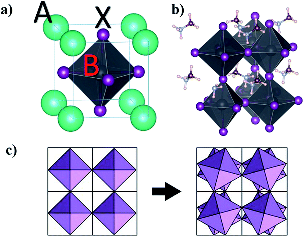 | ||
| Fig. 1 Schematic illustration of (a) ABX3 cubic perovskite in which A and B cations together with X anions occupy the vertices and body-centred and face-centred positions, respectively, and (b) tetragonal unit cell of the MAPbI3 perovskite with different orientations of MA cations. (c) Cubic to tetragonal transition showing broken symmetry by tilting of the octahedra from the top view. | ||
Depending on the radius of cations and anions in a close-packed arrangement, the structure might deform to tetragonal, orthorhombic and layered structures that can be determined by a geometrical tolerance factor t defined as
 | (1) |
Cubic, tetragonal/orthorhombic and 2D layered structures can be obtained from the geometrical terms with tolerance factors of 0.9 < t < 1, 0.7 < t < 0.9 and t > 1, respectively. A second criterion comes from the quantum mechanical considerations of Pauling rules taking into account the coordination number and cation/anion radius ratios,30 while more detailed chemical bonding effects need to be considered for optoelectronic properties.
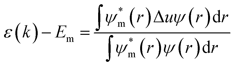
In the metal halogen perovskite structure, the chemical bonding between the metal and the halogen is determinant for the bandgap and the dispersion of the energy bands in the material. Higher electronegativity differences result in more ionic bond character in which the electron cloud is less dispersed along the bond and more localized close to the nuclei; and as a result shorter bond lengths and higher band gaps with less dispersive electronic band structure close to the band edges are obtained. The dependence of the bandgap on the electronegativity of the cation and anion in perovskite structures has been reported previously.32–34 This dependency can be rationalized by the ionicity or covalency of the chemical bond with implicitly affects the chemical bond length as well as the electron localization. The dependency of the bandgap of lead halogen perovskites on the lattice constant (which is directly related to the chemical bond length of the lead and halogen in the cubic/tetragonal lattice) and the dependency of the bandgap of a series of lead-free perovskites on the electronegativity of metal are presented in Fig. 2a and c.
 | ||
| Fig. 2 (a) Dependence of the perovskite bandgap on the pseudo-cubic lattice constant. Reproduced from ref. 42 with permission of the Royal Society of Chemistry. (b) Dependence of the APbI3 perovskite bandgap on the geometrical factors due to the steric effects from the A-cation. Reprinted with permission from Springer Nature, Nat. Commun., 2014 (ref. 35). (c) Dependence of the MABI3 perovskite bandgap on the electronegativity of the metal cation (B). The data are collected from different theoretical or experimental studies reported in ref. 34, 38, 40 and 43–46. The line is a guide for the eye. | ||
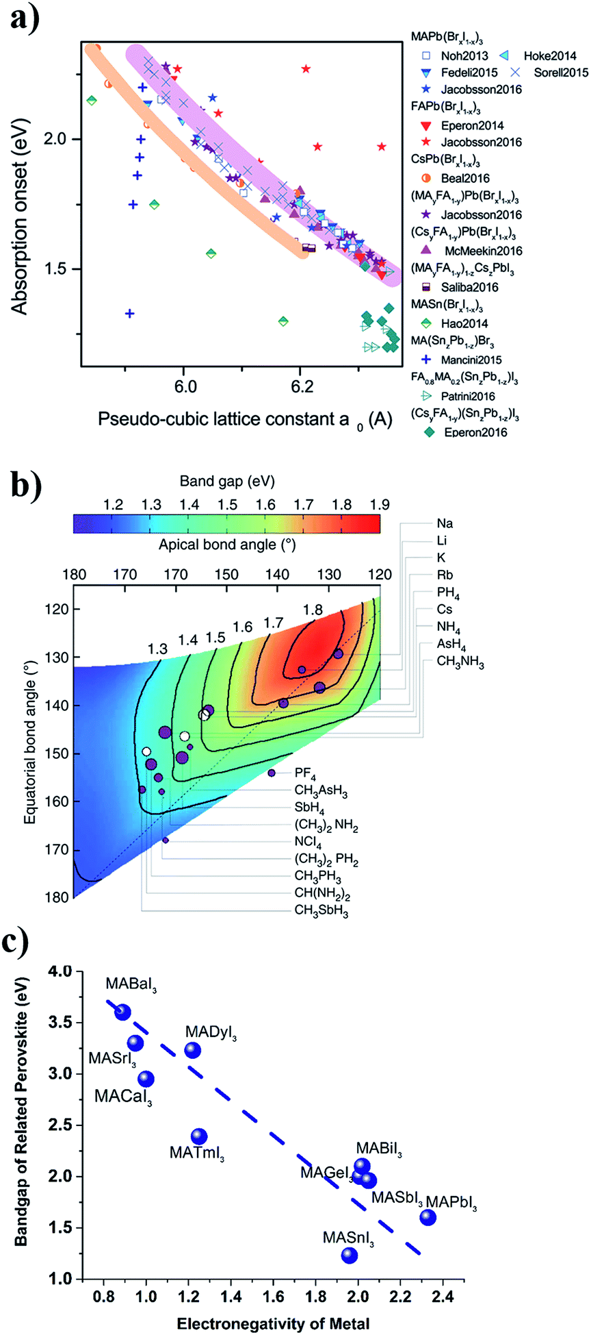
An additional dependence comes from the geometrical factors affecting the details of the symmetry in the lattice; a smaller monovalent cation will distort the cubic structure by tilting the octahedrons resulting in a tetragonal symmetry with angles between the different octahedral layers as depicted in Fig. 1c. A simple tight binding model description is instructive to explain the general trends in the bandgap of perovskites with
 | (2) |
 the atomic wavefunction, Δu the perturbation potential coming from the interaction of atoms, and ψ(r) the total atomic wavefunction for the periodic electronic state34,35 at position r. For lead iodide perovskites, by tilting the PbI6 octahedra, both the bottom CB, consisting of the antibonding negative integral of I6s and Pb6p states, and the top VB (antibonding negative overlap of Pb6p and I5p states) change due to the different orbital overlaps.36 The main effect of the tilting of the octahedra is thus to modify the overlap of atomic orbitals between the metal and halogen with a resulting change in the bandgap. Utilizing this effect for band gap control can be denoted steric engineering and has been implemented in lead halide perovskite materials for band gap tuning by implementing different monovalent cations in the structure (Fig. 2b).35
The main approach that has been used to theoretically estimate the bandgap of metal halide perovskites so far is the implementation of DFT calculations based on GGA functionals. The reason is that the common band gap underestimation using a GGA approach is absent for many of the lead perovskite materials. A large part of this comes from an error cancelation where neglection of spin orbit coupling (SOC) and the absence of exact exchange in modelling of halide based perovskite solar cell materials reproduce band gaps very close to experimental values. For lead and tin perovskites, inclusion of spin orbit coupling (SOC) into the calculations will narrow down the band gap while hybrid functionals or the GW-approximation will overestimate the band gap.37 GW calculations that include SOC effects instead result in a theoretical band gap again closer to the experimental values which supports an error cancelation.37 The exact reason for the error cancelation, however, is un-clear where for example the amount of the error cancelation is different for Bi and Pb which have a very similar angular momentum quantum number for outer shell electrons.38 Given that the GGA approach reproduces the experimental band gaps of many of the materials as well as the apparent details of the experimental dispersion and DOS,38–40 it represents a convenient screening approach where the full inclusion of SOC effects using hybrid functionals or the GW-approximation is advised for a full investigation of the compounds at a later stage.
Other properties such as the dielectric constant, the absorption coefficient (α), the charge carrier mobility (μ), and the exciton binding energy (EB) should be considered for the evaluation and analysis of photovoltaic materials. They are in turn related to the device operation via the charge separation efficiency, the charge carrier diffusion length, L (L depends on μ), and charge generation and collection efficiency (related to α/L).
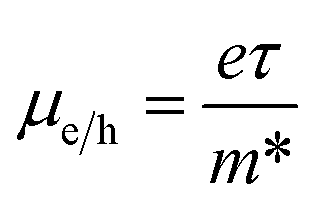
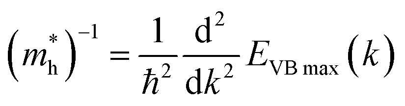
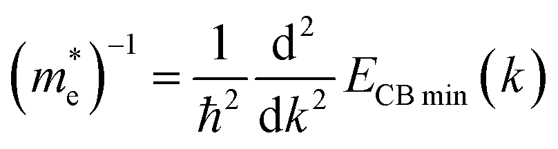
The mobility of charge carriers (μ) within the effective mass approximation can be described by:41
 | (3) |
 | (4.1) |
 | (4.2) |
The absorption coefficient is directly proportional to the dipole strength of electronic transitions, the number of available states for light-induced electronic transitions and thus the number density of polarizable electrons per unit volume. The dipole strength is proportional to the transition dipole moment μ which is defined by:
 | (5) |
 , ψi, e, r and v are the wavefunction of the final orbital and initial orbitals engaged in electronic transition, elementary charge of electrons, the location of the electron and the volume of the unit cell. Two dimensional materials show a better stability but lower light absorption due to the lower number density of metal/halogen atoms and thus electrons per volume that can be active for light absorption and thus results in a lower absorption cross-section.
Moreover, to have an effective charge separation in the solar cell, the exciton binding energy should be low or be effectively broken by the field from the contact materials to produce more free charger carriers than bound excitons. The exciton binding energy (Ebin) is proportional to (m*/ε):
| Ebin ∝ (m*/ε) | (6) |
Before reviewing the recent efforts for new perovskite solar cell materials based on metal exchange within the lattice of MAPbI3, more details of the crystal structures and the relevant physical properties of the mother compound are presented in the following section.
3. Lead iodide perovskite materials
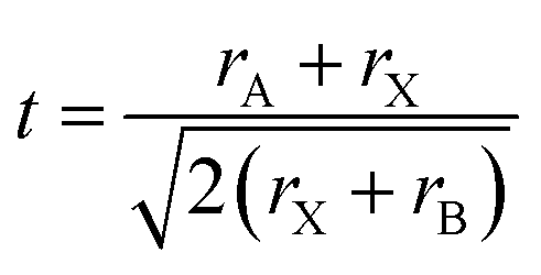
MAPbI3, the main compound of the ABX3 perovskite solar cell family, has a tetragonal perovskite phase at room temperature. The corresponding tetragonal lattice constants are approximately a = 8.84 and c = 12.64 angstrom with the space group I4cm;47 however, the reported lattice constants in experimental and theoretical research show slight variations depending on the growth method/conditions or calculation details.14,47–49 A phase transition from tetragonal to cubic symmetry occurs at 55 °C for single crystals47 and 54 °C for polycrystalline films49 with a cubic structure having a lattice constant of 6.31 angstrom and the space group of P4mm.47 The space group symmetries of I4/mcm and Pm![[3 with combining macron]](https://www.rsc.org/images/entities/char_0033_0304.gif) m for the tetragonal and cubic phases of MAPbI3 are also reported,50 where the unit cell symmetry is dependent on the orientational ordering of methylammonium (MA) cations50,51 within the unit cell. Taking the rotational freedom of the MA cations at room temperature into account, with flipping on picosecond time scales,52 one should consider a thermal-average structure rather than a specific fixed structure at room temperature when one compares the simulated and experimental X-ray diffraction (XRD) data.30
m for the tetragonal and cubic phases of MAPbI3 are also reported,50 where the unit cell symmetry is dependent on the orientational ordering of methylammonium (MA) cations50,51 within the unit cell. Taking the rotational freedom of the MA cations at room temperature into account, with flipping on picosecond time scales,52 one should consider a thermal-average structure rather than a specific fixed structure at room temperature when one compares the simulated and experimental X-ray diffraction (XRD) data.30
A schematic illustration of the MAPbI3 tetragonal unit cell is presented in Fig. 1b in which the lead iodide inorganic octahedrons are surrounded by MA cations with different orientations. Depending on the orientation and the type of the cation, the presence of defects and impurities and observed photo-induced structural changes, the PbI6 octahedra experience different tilting or distortions that modify the physical properties and photovoltaic performance.
Inorganic CsPbI3 and CH(NH2)2PbI3 (formamidinium lead iodide – FAPbI3) are two other relevant compounds that have been investigated extensively. The corresponding photovoltaic phases at room temperature are cubic with Pmm symmetry and a lattice constant of 6.36 angstrom for FAPbI3 (ref. 53 and 54) and 6.17 angstrom for CsPbI3.55 At room temperature, the cubic CsPbI3 is only stable in the absence of air and otherwise it transforms to an orthorhombic yellow phase which can be transformed back to the black phase at 310 °C.55
The success of the MAPbI3 in solar cell devices can, at least in part, be ascribed to strong light absorption, long charge carrier diffusion lengths, low-density of detrimental defects, and very low exciton binding energy, collectively leading to high photovoltages, and near 100% internal quantum efficiencies (IQE) within the device.56 Based on the choice of the monovalent A-site cation, a wide range of bandgaps can be achieved for lead iodide perovskites due to the geometrical factor described above (Fig. 2b).35 A summary of relevant physical properties for the three main compounds MAPbI3, CsPbI3 and FAPbI3 is compiled in Table 1. It should be noted that the single crystal values might be different from the reported polycrystalline based values, which in turn are more relevant and realistic for material properties as applied in devices. The latter could vary with the precursor quality and the precise crystallization procedure during film preparation.
| a m 0 is the free electron mass. b 7.1 from DFT calculations and 60–70 from experimental measurements. c Calculated by time resolved PL quenching for electrons. d Measured from nanocrystals. e Depends on the excitation fluence. f Calculated by DFT in ref. 81 which is in agreement with other studies and experimental predictions. g From GW calculations. h From DFT calculations; Cs and MA lead iodine have the same dielectric constant. i Measured from 12 nm nanocrystals. j Calculated by DFT in ref. 67. k Total mobility measured experimentally, assuming that electron and holes have similar contributions in this number. l Roughly estimated from the lifetime and mobility data of small quantum dots in ref. 65 considering the Einstein relation. m Lead: cation radius (Pb2+): 137 pm, electronegativity: 2.33. | |||
|---|---|---|---|
| Parameters/material | MAPbI3 | FAPbI3 | CsPbI3 |
| Crystal structure | I4/mcm (tetragonal)50 |
Pmm (cubic)59 |
Pmm (cubic)55 |
| Optical band gap | 1.6 eV (ref. 43) | 1.48 eV (ref. 43) | 1.73 eV (ref. 55) |
| Static dielectric constant | 60–70 (ref. 1 and 60)—7.1b37 | 49.4 (ref. 59) | 8h61 |
| Hole mobility | 0.6–1.4 cm2 V−1 s−1 (ref. 62) | 3.5 (ref. 63) and 27 cm2 V−1 s−1 (ref. 64) | 2 cm2 V−1 s−1k65 |
| Electron mobility | 0.06–1.4 cm2 V−1 s−1 (ref. 62) | 0.2 cm2 V−1 s−1 (ref. 63) | 2 cm2 V−1 s−1k65 |
| Electron effective mass | 0.10m0a,g66 | 0.09m0a66 | 0.13m0a,j67 |
| Hole effective mass | 0.10m0g68 | 0.18m0g,j67 | 0.17m0g,j67 |
| Diffusion length | 1 μm (ref. 69) | 813 nmc43, 6.6 μm (ref. 59) | 1.7 μml |
| e–h recombination lifetimee | 5 ns (ref. 70) | 453 ns (ref. 71) | 20 ns (ref. 72) |
| Absorption coefficient | 3 × 105 cm−1 (ref. 1) | 4 × 105 cm−1 (ref. 73) | 2.5 × 105 cm−1 (ref. 72) |
| Exciton binding energy | 2–20 meV (ref. 74) | 10 meV (ref. 66) | 20 meVi75 |
| Density of sub-bandgap/trap states | 1015 to 1016 cm−3 | 1.13 × 10⁻¹⁰ cm−3 (ref. 59) | >4 × 10¹⁶ (ref. 76) |
| Time scale for e-transfer to selective constant | Symmetric for e/h sub-picosecond77 | — | — |
| Time scale of carrier coolinge | 1 ps (ref. 78) | 1–40 psd79 | A few 10 ps (ref. 80) |
| Time scale of defect migrationf | 300–1000 meV (ref. 81) | 200–1200 meV (ref. 81) | 200–1400 meV (ref. 81) |
4. Lead exchange with divalent metals
4.1 Tin and germanium perovskites
Historically, CsSnI3 has been used as a hole conductor in solid state dye sensitized solar cells due of its high hole conductivity, first in 2012, before the emergence of solid state hybrid perovskite solar cells.82 Among the first reported lead-free perovskite solar cell devices were devices based on tin which is the closest neighbour of lead in the periodic table with the closest cation radius and electronegativity. The bandgap and carrier effective masses are lower than those of its lead counterpart due to a lower electronegativity of tin compared to lead which can make a more covalent and less ionic chemical bond with halogen atoms.37 Another difference is the magnitude of the spin orbit coupling that is higher in lead compared to tin perovskites37 due to the higher angular momentum of the outer shell electrons in lead.The lower bandgap of tin perovskites leads to a lower maximum open circuit voltage from the device; the theoretical limit for the short circuit current, however, has a current density a bit over 40 mA cm−2 for MASnI3 in comparison to the corresponding value of about 26 in MAPbI3 devices.37 The near 30% theoretical limit for the PCE in devices based on MASnI3 and CsSnI3 (ref. 83) is similar to the lead counterpart MAPbI3.
The calculated tolerance factor for MASnI3 and CsSnI3 structures is 0.92 (ref. 31) and 0.91 (ref. 84) respectively. MASnI3 has a cubic lattice with Pm3m symmetry and a lattice constant of 6.24 angstrom at room temperature85 with an optical bandgap of 1.23 eV. MASnI3 crystalizes at room temperature immediately after spin coating of the precursor solution.44 Efficiencies over 6% and open circuit voltages over 0.88 V have been reported.44 There are stability issues for tin based perovskites which are related to the different oxidation states of Sn and the unstable situation in air or situation with residual oxygen, where all the device fabrication as well as characterization procedures should be performed under air- and oxygen-free conditions and the device should be encapsulated well.86 CsSnI3 with a bandgap of 1.3 eV has shown an enhanced stability in a recent report83 and PCEs up to 4.8% have been reported.87 FASnI3 can be stable up to 210 °C (ref. 88) and is able to reach comparable PCEs as other tin iodide perovskite solar cell materials.89 The phase stability of tin iodide perovskites has been discussed in ref. 44, 88 and 90. The issue of toxicity for tin and lead perovskites has been investigated in ref. 91, where tin is considered less toxic than lead for the human body but considered more toxic for marine animals and fish.
Bandgap tuning of tin perovskites can be achieved with mixed composition compounds with different mixtures of cations/anions. The size of the monovalent A-site cation can alter the bandgap of metal halide perovskites through steric effects,35 as outlined in the framework of tight binding theory: the tilting of for example PbI6 octahedrons leads to different orbital overlaps between lead and iodide and affects the bandgap.35 In tin perovskites, however, due to the smaller size of tin cations, different monovalent cations affect the bandgap mainly by modifying the lattice constant of the perovskite and enabling bandgaps between 1.24 eV and 1.56 eV by monovalent cation engineering.92 Using different monovalent cations and mixtures of different halides, bandgaps between 1.24 eV and 3.0 eV are theoretically predicted for tin perovskites where a mixture of tin and lead perovskites can cover the absorption up to 1060 nm.93,94 For tin based perovskites with the MA monovalent cation, mixed halide compositions can provide bandgaps between 1.2 eV and 1.8 eV (ref. 48).
A mixture of FA and MA cations has resulted in 8.1% PCE95 and a mixture of I and Br anions reach a PCE over 6% (ref. 96) for Sn-based perovskite solar cells. 12.6% (ref. 97) PCE has been achieved in a device based on a lead![[thin space (1/6-em)]](https://www.rsc.org/images/entities/char_2009.gif) :tin mixture composition. The present record efficiency of 17.8% has been reported for a mixed tin:lead perovskite with composition: MA0.4FA0.6Sn0.6Pb0.4I3 (ref. 92).
:tin mixture composition. The present record efficiency of 17.8% has been reported for a mixed tin:lead perovskite with composition: MA0.4FA0.6Sn0.6Pb0.4I3 (ref. 92).
Germanium is the second closest element to lead in the periodic table with oxidation state 2+, has a lower cationic size and lower electronegativity. The toxicity of germanium is relatively low98 and it has therefore been one of the projected candidates for lead replacement. The spin orbit coupling (SOC) has a very small effect on the germanium based perovskite properties compared to tin and lead due to the lower angular momentum of outer shell electrons.99,100 The Goldschmidt tolerance factor of the germanium perovskites MAGeI3 and MAGeBr3 is 0.99 and 1.00, respectively. The crystalline phase at room temperature has a trigonal lattice with R3m symmetry and a = 8.8(8.4) and c = 11.5(10.9) angstrom for MAGeI3(MAGeBr3)99 and the perovskites are thermally stable up to 150 °C.45 By heating the samples, no phase transition to the cubic phase has been reported and the tolerance factor here doesn't include distortions from the electronic contributions.45 Inorganic CsGeI3 also has a trigonal phase with a bandgap of 1.62 eV (ref. 45) which can be transformed to a cubic phase at 277 °C (ref. 101), where the defect physics of CsGeI3 is investigated in ref. 102. Changing the size of the A-site cation as in RbGeI3, the cubic structure adopts a m3m symmetry.100 Devices based on germanium perovskite materials are not developed to the same degree as solar cell devices based lead and tin compounds and the complication in device engineering is connected to air instability issues and complication with different oxidation processes45,103 and the reported efficiencies are so far in the range of 0.1–0.2%. CsGeI3 perovskites have a similar theoretical PCE limit to MAPbI3 with around 31% due to their similar bandgap if one neglects differences in charge carrier mobility and the ability to create trap states. A more realistic estimation would instead place the maximum PCE for germanium based perovskite solar cells at significantly lower efficiency compared to the device efficiency limit for MAPbI3.
Bandgap tuning of germanium based perovskites is pursued by utilizing different monovalent cations,103 halides99 and mixtures of halides and cations104 leading to bandgaps of 1.3–3.7 eV. Non-cubic germanium perovskite compounds show nonlinear optical properties as reported in ref. 103 and 105. Larger monovalent cations can lead to 2-dimensional germanium perovskites with a higher bandgap and lower absorption coefficient which results in an increased transparency.103,106
Electronic structure studies for several tin and germanium perovskite compounds have been presented in ref. 37, 85, 102, 104, 105 and 107–109. Tin and germanium halide perovskites both have a high extinction coefficient and high dielectric constant similar to lead due to the very similar number density of polarizable electrons per volume, similar metal/halide orbitals for the initial and final optical absorption states and similar shielding effects within the material. A summary of the physical properties from experimental and theoretical studies is presented in Table 2.
| a Calculated by DFT. b Calculated by DFT in comparison to MAPbI3 (8.2 from DFT and 60 from experiments). c Tin: cation radius (Sn2+): 136 pm, electronegativity: 1.96; germanium: cation radius (Ge2+): 87 pm, electronegativity: 2.01. | ||||
|---|---|---|---|---|
| Parameter/material | MASnI3 | CsSnI3 | MAGeI3 | CsGeI3 |
| Crystal structure | Pm3m cubic, a = 6.24 Å (ref. 85) | Pm3m cubic, a = 6.22 Å (ref. 110) | Trigonal R3m, a = 8.8 Å (ref. 45) | Trigonal R3m, a = 8.35 Å (ref. 103) |
| Optical bandgap | 1.23 eV (ref. 44) | 1.3 eV (ref. 83) | 2.0 eV (ref. 45) | 1.62 eV (ref. 45) |
| Electron effective mass | 2.65me (ref. 108) | 0.04–0.57me (ref. 110) | 0.31 (ref. 99), 0.12me (ref. 100) | 0.21–0.42 (ref. 102) |
| Hole effective mass | 1.03me (ref. 108) | 0.07me (ref. 110) | 0.41 (ref. 99) | 0.22 (ref. 102) |
| Dielectric constant | 8.2b37 | 48.2 (ref. 110) | — | 18.6 (ref. 102), 10.5a105 |
| Absorption coefficient | 50–80 × 103 cm−1 (ref. 44 and 108) | — | 250 × 103 cm−1 (ref. 99) | — |
| Exciton binding energy | — | 12 meV (ref. 110) | — | — |
4.2 Alkaline earth metals
According to Goldschmidt rules, several alkaline earth metal cations with oxidation state +2 can replace lead in a tetragonal or cubic perovskite unit cell30 with retained crystal symmetry in which strontium has the closet cation radius to lead. Therefore the main difference would be the electronegativity and outer shell electrons of the metal that forms the dominant partial DOS at the bottom of the CB.39 As mentioned in Section 4, the effect of the electronegativity of the divalent cation in the B-site of ABX3 tetragonal perovskites has been reported previously,32 where a higher electronegativity difference between the divalent cation and anion makes more ionic bonds and results in higher band gaps. In metals, the normal definition of electronegativity from covalent bonding considerations is not well defined and the work function of the alkaline earth metal would instead be a better parameter for the evaluation of the bandgap.39 In a previous paper, we have investigated a series of alkaline earth metals for photovoltaic applications.39Fig. 3a shows the density of states (DOS) for different alkaline earth metal halide perovskites in comparison to lead halide perovskites in which the higher ionic nature for iodine-metal results in a higher band gap. Outer shell electrons have s-character and the electronegativity differences with iodine are high which result in higher bandgaps of 2.9–4 eV (ref. 39 and 111). This can be visualized in charge density profile plots within the unit cell in Fig. 3c and d for a comparison of Sr and Pb based perovskites. Pb–I bonds have more even and higher distribution of electron density in between the atoms compared to Sr–I in which the charge density is located closer to the atomic nuclei (Fig. 3c). Higher bandgaps together with a difference in the charge carrier effective masses for alkaline perovskite materials reveal that they are less suited as photovoltaic materials but can instead be implemented as charge selective layers in an all-perovskite device39 in which the same crystal structure and lattice constant of the selective layer are beneficial for epitaxial perovskite depositions. It is also advantageous for a situation with less thermal and mechanical stress in between the active and charge selective layers at different working temperatures. A detailed variation of the contact material lattice constants can also be used for stress-engineering of the perovskite interface to further tune the optical properties of the active layer, which has been reported for silicon and other potential materials in solar cell applications.112–114 Alkaline earth metals also suffer from high reactivity with humidity and water39 and the sensitivity to humidity is higher compared to the lead perovskite. There are efforts to synthesize the alkaline earth metal based perovskites of CH3NH3BaI3 (ref. 111), CH3NH3CaI3−xClx and CH3NH3CaI3 (ref. 115). Due to the possibility of metal replacement according to Goldschmidt's rules with a retained lattice structure, alkaline earth metal cations can also be used as dopants or for the partial replacement of the lead in the MAPbI3 lattice in perovskite solar cell devices.116–119 Klug et al. investigated different metal dopants in the MAPbI3 structure including divalent metals and monovalent Mg2+ and Sr2+ dopants120 and presented band edge shifts, work function modifications and impacts on crystal growth as a consequence of doping. The band gap of MAPbI3 was not changed but slight peak shifts in the XRD pattern was indicative of doping of the metal cations in the lattice. Mg perovskites have been theoretically investigated and predicted to have a bandgap of 1.7 eV in a 3D perovskite structure despite the smaller cationic radius of Mg compared to Pb2+.121 There are no experimental reports of 3D magnesium halide perovskites yet.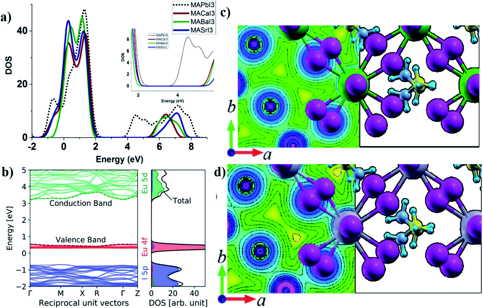 | ||
| Fig. 3 (a) PDOS of alkaline earth metal iodide perovskites in comparison to MAPbI3 showing the effect of electronegativity on the bandgap. Reprinted the figure with permission from ref. 34 Copyright 2016 by the American Physical Society. (b) Band structure and PDOS of MAEuI3 showing the contribution of Eu 4f and 5d orbitals to the top VB and bottom CB. Reproduced from ref. 40 with permission from the Centre National de la Recherche Scientifique (CNRS) and the Royal Society of Chemistry. A comparison of chemical bonding effects in charge density plots of (c) MASrI3 and (d) MAPbI3. Reprinted with permission from ref. 30 Copyright 2015 American Chemical Society. | ||
4.3 Lanthanides and actinides
Lanthanide and actinide cations of Eu2+, Dy2+, Yb2+, Tm2+ and Np2+ can according to Goldschmidt rules replace Pb2+ within the tetragonal perovskite lattice. Most of the lanthanides are non-toxic or less toxic than lead and rather abundant, i.e., more abundant than Pt, Ru, gold and even iodine.40 Regarding a vapor deposition scheme of lanthanide compounds, most of them have a temperature similar or close to the lead system vapor temperature. The difference between different lanthanides comes from the number of f-electrons which does not contribute the outermost shell electrons apart from screening effects. The VB and CB edges in lanthanide iodide perovskites consist of lanthanide f-electrons and d-electrons respectively and the main valence to conduction band electronic transition for MAEuI3 is thus based on a local inner atom transition within the La atom (Fig. 3b). Therefore, the optical absorption onset would be rather inert with respect to quantum confinement effects.20,40 By choosing larger monovalent cations, 2-dimensional layered perovskite structures can be obtained, i.e., (C4H9NH3)2EuI4.122 So far, experimental and theoretical efforts have investigated a series of lanthanide based perovskite materials such as MAEuI3,20,40 MAYbI3,40 MADyI3,40 MATmI3,40 and (C4H9NH3)2EuI4 (ref. 108) in which the lanthanum has a 2+ oxidation state; 3+ oxidation states of lanthanides can be adopted for a double perovskite structure as discussed in Section 6 trivalent metal substitution and in ref. 123.4.4 Transition metals
Transition metals have multiple oxidation states that introduce stability issues similar to the ones mentioned for tin and germanium perovskites. They are abundant elements and have a smaller cation radius than lead. Therefore, according to Goldschmidt rules, smaller monovalent A-site cations should be implemented together with transition metals in order to form a 3-dimensional perovskite and otherwise they form 2-dimensional layered perovskites which have directional charge transport and a lower light absorption cross section compared to 3D perovskites. In addition, some of the transition metals such as Cd and Hg are highly toxic and even more toxic than lead. Although the research is progressing for transition metal halide perovskites, the photovoltaic capabilities of this family of materials have so far been less promising than lead halide perovskites.MA2CuClxBr4−x forms a layered monoclinic/orthorhombic perovskite structure in which metal halide octahedral layers are separated by the MA cations. The band gap can be tuned with different halide ratios as discussed in Section 4. Cortecchia et al. investigated a series of such compounds with tuneable band gaps where a low light absorption and heavy hole effective mass due to the reduced dimensionality were likely part of the reason for the initial poor device efficiency of about 0.01%.124 MA2PdCl4 is a similar compound with a band gap of 2.2 eV, which forms a 2D layered perovskite structure.125 (3-Pyrrolinium) CdCl3 forms a stable layered ferroelectric perovskite at room temperature, which could reach a Voc of 32 V in a simple architecture, but due to a very low current cannot be considered implementable in a full working photovoltaic device.126
Cui et al. synthesized layered copper bromide perovskites with different A-cations in a solution-processed approach which reach a bandgap of 1.74 eV and an efficiency of 0.6% in an initial solar cell device application.127 Due to their multi-valency and multiple oxidation states, transition metal monovalent cations and trivalent cations have been implemented for doping of MAPbI3 (ref. 128 and 129) and for the formation of double perovskites130 as described in Sections 5 and 6.
An upcoming family of ABX3 perovskite structures consists of divalent transition metals at the B site, alkaline earth metals at the A site and S2− or Se2− at the X site, called chalcogenide perovskites. A series of such compounds have been investigated by DFT calculations in ref. 131 and 132 in which some of them show promising device potentials and narrow bandgaps, i.e., CaZrSe3 and BaZrS3. The modification of chalcogenide perovskites with replacement of alkaline earth metals with MA+ seems promising to form a stable perovskite structure.132 In these compounds, the main contributions to the density of states at the VB and CB edges mainly originates in orbitals from S/Se and the divalent transition metal, respectively.
Table 3 summarises the physical properties of some divalent metal iodide perovskites for solar cell applications.
| Material/property | Crystal structure | Band gap | Electronegativity | Divalent cation radius |
|
|
|---|---|---|---|---|---|---|
| a Values for lanthanides and alkaline earth metals are reported from DFT calculations by metal replacement in the tetragonal unit cell of MAPbI3. Effective mass of charge carriers of the alkaline earth metals extracted for Γ to R. For lanthanides the effective masses are averaged in 3 different directions within the reciprocal lattice. For the transition metal halide perovskites, the effective masses are reported within the ab-plane of the layered structure. | ||||||
| MACaI3 (ref. 34) | I4/mcm (tetragonal) | 2.95 eV | 1.00 | 120 pm | 0.41me | 9.6me |
| MASrI3 (ref. 34) | I4/mcm (tetragonal) | 3.30 eV | 0.95 | 135 pm | 0.41me | 9.6me |
| MABaI3 (ref. 34) | I4/mcm (tetragonal) | 3.60 eV | 0.89 | 152 pm | 0.41me | 9.6me |
| MAEuI3 (ref. 40) | I4/mcm (tetragonal) | 2.68 eV | 1.2* | 134 pm | 0.54me | 3.8me |
| MAYbI3 (ref. 40) | I4/mcm (tetragonal) | 1.98 eV | 1.25* | 122 pm | 0.28me | 4.3me |
| MADyI3 (ref. 40) | I4/mcm (tetragonal) | 3.23 eV | 1.22 | 127 pm | 1.13me | 3.04me |
| MATmI3 (ref. 40) | I4/mcm (tetragonal) | 2.39 eV | 1.25 | 123 pm | 0.28me | 3.94me |
| MA2CuCl4 (ref. 124) | P121/a1 (monoclinic) | 2.48 eV | 1.9 | 87 pm | 0.31me | 1.71me |
| MA2FeCl4 (ref. 133) | I4/mmm (tetragonal) | — | 1.83 | 75 pm | — | — |
| MA2PdCl4 (ref. 125) | Layered Ruddlesden–Popper | 2.22 eV | 2.2 | 100 pm | — | — |
5. Lead partial exchange with monovalent metals
Monovalent metals cannot replace lead in the perovskite structure without charge compensation according to Goldschmidt's rules; they can partly be incorporated into the lattice, however, as dopants in lattice or interstitial sites. The motivation for such an incorporation is to modify the material properties, i.e., to enhance the charge mobility and conduction. The presence of such additives can change the local distortion of the nearest PbI6 octahedra and affect the defect density or shift the bands. Abdi-Jalebi et al. implemented monovalent cation additives (Cu+, Ag+ and Na+) in the precursor solution of MAPbI3 in order to balance the hole and electron conductivities in the material. They reported an enhanced voltage and current for AgI and NaI additives which was attributed to a better crystal growth and enhancement of the bulk charge transport.129 Related DFT calculations further show that the formation energy of the interstitial incorporation and doping is negative and there are no new intra-band gap states introduced after the incorporation. X-ray Photoelectron Spectroscopy (XPS) data confirm the presence of additives in the prepared film and interfaces as well as a band shift; however, it is not clear yet whether they are incorporated as dopants or not. Shahbazi et al. reported an enhanced hole extraction and device efficiency by the addition of AgI to the precursor solution128 and Yang et al. reported increased p-type conductivity in MAPbI3 after the addition of NaI to the precursor solution.134 Additional monovalent cation precursors, i.e., CsI, KI and RbI, are implemented in a recently reported cation cascade mixed perovskite135 with enhanced stability and performance in which they are supposed to replace the A-site MA+ or formamidinium (FA+) cations in the perovskite lattice. Other divalent and trivalent dopant additives have been implemented136 to modify the material properties although it is not clear in all the cases if the dopants are accumulated at interfaces or in the bulk of the perovskite acting as a dopant or interstitial defect modifier. A combination of monovalent and trivalent cations can replace the lead in a double perovskite lattice that is described in the next section together with the situation for trivalent cations.6. Lead exchange with trivalent metals
Bi3+ has been the most investigated trivalent metal cation for lead exchange in halide perovskite solar cell applications so far. Because of the oxidation state of 3+ and its chemical bonding preferences it cannot fit within the tetragonal structure and a hexagonal structuring result in A3Bi2I9 (A = Cs or MA; space group P63/mmc137) with face sharing BiI6 octahedra and lattice constants a = 8.39 angstrom and c = 20.98 angstrom (presented in Fig. 4a). The VB edge states consist of iodine states and the lowest states in the CB consist of hybridized bismuth–iodine states and a second CB with a 500 meV gap with respect to the first CB which consists mainly of Cs states.38 Bismuth perovskite materials also show very high Born effective charges138 and can be produced by both solution processed139 and vapour deposition techniques.140 There is a phase transition at 160 K to a monoclinic crystal structure with the space group C2/c.137 So far, different monovalent cations such as potassium,138 caesium,139 rubidium,138 methylammonium139 and guanidium141 have been implemented in bismuth halide perovskite materials. The chemical bonding in the unit cell is formed in a way that there is a good continuity in the charge density planes within the ab-plane and on the other hand, there is no bonding between the Bi–I networks in the direction of the c-axis resulting in a layered perovskite with directional charge transport38 (Fig. 4a). The layered structure with a bandgap of 2.2 eV (ref. 38) is considered to have less toxicity and enhanced stability140 compared to the 3D lead perovskite. The rather large bandgap value, however, limits the highest obtainable PCE from single bandgap devices and instead makes the material more suitable for tandem applications. The band dispersion shows directional transport where the flat bands correspond to high intrinsic effective masses in the out of plane directions (Fig. 4b).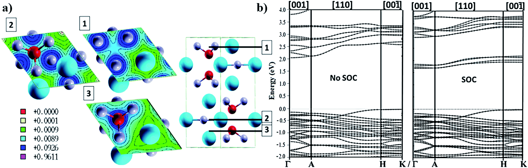 | ||
| Fig. 4 (a) Charge density planes within the hexagonal unit cell of Cs3Bi2I9 perovskite illustrating the continuous density within the ab-plane and a non-continuous profile along the c-axis. Band structure of the bismuth perovskite calculated by (b) non-SOC DFT and (c) SOC DFT. The bands show good dispersion within the ab-plane and very flat behaviour in the directions along the c-axis. Reprinted with permission from ref. 38 Copyright 2016 American Chemical Society. | ||
SOC effects are pronounced in the electronic structure for bismuth compounds, although the amount of SOC split is lower than that in the lead compound counterpart. In addition to the limited directional transport, a lower dielectric constant, higher exciton binding energy, and lower absorption coefficient are found compared to MAPbI3 and would limit the expected PCEs where the highest reported efficiency so far is about 1%.142 A high exciton binding energy has been suggested from ab initio calculations due to the low dielectric constant,38 and exciton binding energy values of 300–400 meV have been reported,143,144 from experiment and theory. Apart from solar cell applications, light emitting applications can also be considered in which a higher exciton binding energy is beneficial as, i.e., in MA3Bi2Br9.145
Johansson and co-workers could modify the material by adding excess iodide in the precursors; the new material with the expected formula Cs3Bi2I10 has a bandgap of 1.77 and a significantly higher absorption coefficient than Cs3Bi2I9.146 Further modifications with other cations leads to extended light absorption and higher efficiencies based on AgBiI4 (ref. 147) and Ag3BiI6 (ref. 148) with the highest efficiency of 4.3%.148
Fabian and Ardo et al. implemented a one dimensional structure of hexadecylamine (HDA) bismuth iodide perovskite with the formula HDABiI5 in a device application with 0.02% efficiency, a bandgap of 2.05 eV and good thermal stability up to 200 °C.149 A series of bismuth based one dimensional layered structures have been investigated in ref. 150.
These new materials implement a combination of a monovalent and a trivalent cation in a double perovskite structure with edge sharing octahedra as a consequenceof i.e. silver and bismuth iodide layers (Fig. 5a and b). Turkevych et al. investigated several members in the family with the general formula 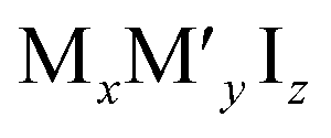 having a rudorffite structure (x + 3y = z if M is monovalent and M′ is trivalent) in which by changing x and y one can change the sequence of edge sharing octahedra.148
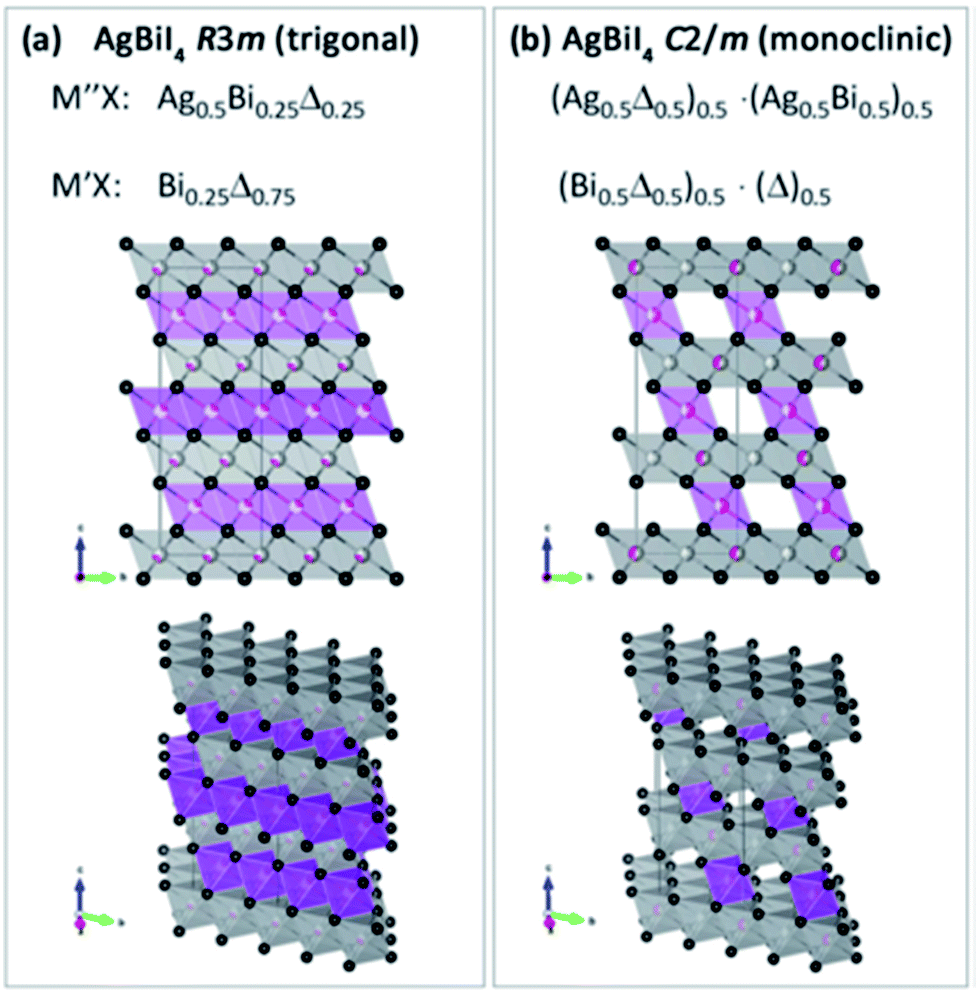 | ||
| Fig. 5 Schematic of the lattice for the layered AgBiI4 double perovskite with (a) trigonal and (b) monoclinic symmetries. Purple and grey octahedral layers correspond to bismuth and silver iodide octahedra, respectively. Reprinted with permission from ref. 148 2017 Wiley. | ||
Another series of A3B2X9 double perovskites includes gold and toxic thallium based perovskites in which the metal has two oxidation states and can occupy monovalent and trivalent oxidation states simultaneously and replace lead in two consequent octahedra with mono- and trivalent metals in a layered double perovskite lattice.151
Antimony is a neighbour of Bi in the periodic table with oxidation state 3+ and a smaller cationic radius. In similarity to bismuth, the antimony cation tends to form layered perovskites with the formula A2Sb3X9. By choosing different monovalent cations (A) the dimensionality of the antimony perovskite can be controlled to be zero-, one- and two-dimensional structures. Different monovalent cations of Cs+,46 Rb+,152 MA+153,154 and N(CH3)4 (ref. 155) have been employed and depending on the growth method result in 3D, 2D, 1D, and 0D perovskite structures respectively. For photovoltaic applications mainly Cs3Sb2I9, Rb3Sb2I9 and MA3Sb2I9 (corresponding space groups of P63/mmc46,143 and P1c1 (ref. 152)) have been investigated46,152,153 and efficiencies of up to 0.66%, Voc of up to 0.89 V and current densities of around 2 mA cm−2 have been obtained. The bandgap is close to 2 eV or slightly more than 2 eV depending on the monovalent cation and the absorption coefficient can be as high as 105 cm−1.46,152,153
Another important family of double perovskites includes A2BB′X6 (ref. 156) in which A = MA/FA/CS, B = Sb3+/Sn3+, B′ = Cu+/Ag+/Au+ and X = Cl/Br/I. And it is possible to modify the structure by replacing B′ with a vacancy to form an A2BI6 structure.157 Cs2AgBiBr6 (ref. 158), Cs2Pb2Br6 (ref. 158) and Cs2PdBr6 (ref. 157) are examples showing interesting photovoltaic characteristics for device applications. Here, the main contributions to the VB and CB edges are from halide and metal orbitals, respectively. For example, Cs2PdBr6 has a promising 1.6 eV bandgap with rather low hole and electron effective masses and shows water resistance properties. A series of double perovskites have been explored in ref. 130, 158 and 159 by DFT calculations. There are a wide variety of double perovskite compounds with a combination of mono- and trivalent cations with interesting properties such as suitable band gaps and potentials for photovoltaic applications; so far, however, there has been no double perovskite material found that can compete or replace lead in MAPbI3. We refer the reader to ref. 151 for further information about double perovskite structures. Other routes utilize cation addition by cation doping where Snaith and co-workers implemented Al3+ doping for MAPbI3 based devices and have reached a PCE of 19.1% with a high PL quantum yield.120 In another study, by Abdelhady et al., Bi3+, In3+ and Au3+ incorporation in the MAPbI3 perovskite structure has been shown to tune the band gap and enhance the conductivity of charge carriers.160
A summary of selective physical properties of Bi and Sb based perovskite solar cell materials is presented in Table 4.
| Cs2Bi3I9 | MA2Bi3I9 | Cs3Sb2I9 | |
|---|---|---|---|
| a Bismuth: cation (Bi3+) radius: 110 pm, electronegativity: 2.02; antimony: cation (Sb3+) radius: 90 pm, electronegativity: 2.05. | |||
| Crystal structure | Hexagonal38 | Hexagonal38 | P63/mmc (hexagonal)46 |
| Band gap | 2.0 eV (ref. 38) | 2.1 eV (ref. 38) | 1.96 eV (ref. 46) |
| Electron effective mass | 1me (ref. 38) | 0.54me (ref. 38) | 0.62me (ref. 46) |
| Hole effective mass | 1.1me (ref. 38) | 0.95me (ref. 38) | 0.68me (ref. 46) |
| Static dielectric constant | 9.1 (ref. 38) | 9.6 (ref. 38) | — |
| Absorption coefficient | 7 × 104 cm−1 (ref. 38) | 9 × 104 cm−1 (ref. 38) | 2 × 105 cm−1 (ref. 46) |
| Exciton binding energy | — | 300–400 meV (ref. 143 and 144) | — |
7. Concluding remarks
The field of lead based perovskite solar cell materials is developing fast and recently, highly efficient devices with improved stability have been presented. On the other hand, lead free materials can be environmentally friendly alternatives with the added benefit of an increased span of available bandgaps and charge carrier anisotropies also opening for a wider set of applications such as utilization as charge selective layers and standalone or tandem configuration light absorbers as well as utilization in light emitting applications. Lead based perovskites are still the champions for highly efficient devices (>22%), where lead-free perovskite materials still show lower PCEs (<10%). Tin, germanium and bismuth are the most investigated lead free perovskites with interesting properties. Important parameters for device applications such as a suitable bandgap, high absorption coefficient, high dielectric constant, high charge carrier mobility, low defect density, and device stability have so far not been all been fulfilled by lead free perovskite materials. With the emerging knowledge of the inter-dependencies of the constituent elements and their bonding effects on their crystal structure, exciton binding energy, bandgap and light absorption partly understood, progress in further improvement of material properties and their application in different fields is expected. Gathering the theoretical and experimental knowledge of these new systems, considerations of different steric effects coming from ionic radii and atomic orbital overlaps, and attention to the electronegativity and work function of the metal and different chemical bond lengths to different halogens, the density of available states at VB and CB edges and the band energy dispersion can be understood and controlled. The band dispersion together with the number density and nature of the polarizable electrons are responsible for the absorption coefficient and the intrinsic charge carrier mobility. Mixed cation/anion lead perovskites so far show the best efficiencies (>22%)161 and reported stabilities (stable for 1000 hours at 85 °C and 85% humidity under illumination)162 and a wide range of band gaps and tuneable properties can be obtained with different mixtures of Br/I and MA/FA constituents.27 However, as mentioned in Section 1, there is still a need to explore lead free perovskite solar cell materials. For lead free compounds, further bandgap tuning is feasible based on different monovalent cations or anions implemented in the structure rather than the properties of the metal cation such as electronegativity and the radius (see Section 4). The reported bandgaps for different lead free perovskite compounds can be further tuned by monovalent cation engineering as previously implemented for lead based compounds. Although the monovalent cation has no contribution in the VB and CB edge electronic states, the steric effects from different A-site cations change the tilting of the metal–halogen octahedra and consequently affect the bandgap.35In 2D layered perovskites with a lower number density of available metal–halogen octahedra per unit volume, light absorption cross-section is smaller than that of 3D materials and they show a natural charge carrier anisotropy due to their lower dimensionality. Lanthanide perovskites have a local interatomic near band edge light absorption arising from lanthanide d and f states which results in strong luminescence. In the 2D structures there are also combinations of electronic and structural effects, where e.g. d-orbital dominated CB edges and layered structures with less connectivity between the metal halogen octahedra result in lower dispersion in the electronic band structure and higher effective mass and lower mobilities.
Lanthanide based halide perovskites have special luminescence; metal halide perovskites based on alkaline earth metals have a relatively high bandgap making them less suitable as a photoabsorber but can instead be used as charger selective layers with benefits of a similar lattice structure to the light absorber in an all-perovskite solar cell device. Monovalent and trivalent metals are adopted in double perovskite structures or as additives to perovskite precursors to modify the growth and enhance the desired physical properties of MAPbI3. Progress is made by strategies to further improve the photovoltaic characteristics of lead free materials by enhancing the light absorption and stability together with a combination of 2D and 3D structures to improve the charge mobility through structural modification with a better orbital overlap between the octahedra. The perspective presented in this work surveys the most recent work of new lead free perovskite materials and their physical properties by which a better understanding of the relationships between the different constituent elements and the resulting optoelectronic properties is conjectured to be valuable for the perovskite solar cell field.
Conflicts of interest
There are no conflicts to declare.Acknowledgements
We acknowledge the Swedish Energy Agency, grant number 43294-1, for financial support of this work. Erik Johansson, Gerrit Boschloo, Håkan Rensmo, Jesper Jacobsson, Sagar M. Jain, Jolla Kullgren, Andreas Röckert, Roghayeh Imani, Matthew Wolf and Anders Hagfeldt for their contributions to lead exchange studies and co-authorship in our previous publications.Notes and references
- M. A. Green, A. Ho-Baillie and H. J. Snaith, Nat. Photonics, 2014, 8, 506–514 CrossRef.
- M. Grätzel, Nat. Mater., 2014, 13, 838–842 CrossRef PubMed.
- E. J. Juarez-Perez, R. S. Sanchez, L. Badia, G. Garcia-Belmonte, Y. S. Kang, I. Mora-Sero and J. Bisquert, J. Phys. Chem. Lett., 2014, 5, 2390–2394 CrossRef PubMed.
- E. Strelcov, Q. Dong, T. Li, J. Chae, Y. Shao, Y. Deng, A. Gruverman, J. Huang and A. Centrone, Sci. Adv., 2017, 3, e1602165 CrossRef PubMed.
- J. M. Frost, K. T. Butler, F. Brivio, C. H. Hendon, M. van Schilfgaarde and A. Walsh, Atomistic Origins of High-Performance in Hybrid Halide Perovskite Solar cells, Nano Lett., 2014, 14, 2584 CrossRef PubMed.
- M. Pazoki, T. J. Jacobsson, J. Kullgren, E. M. J. Johansson, A. Hagfeldt, G. Boschloo and T. Edvinsson, ACS Nano, 2017, 11, 2823–2834 CrossRef PubMed.
- Z. Xiao, Y. Yuan, Y. Shao, Q. Wang, Q. Dong, C. Bi, P. Sharma, A. Gruverman and J. Huang, Nat. Mater., 2014, 14, 193–198 CrossRef PubMed.
- H. J. Snaith, A. Abate, J. M. Ball, G. E. Eperon, T. Leijtens, N. K. Noel, S. D. Stranks, J. T. Wang, K. Wojciechowski and W. Zhang, J. Phys. Chem. Lett., 2014, 5, 1511–1515 CrossRef PubMed.
- E. L. Unger, E. T. Hoke, C. D. Bailie, W. H. Nguyen, A. R. Bowring, T. Heumuller, M. G. Christoforo and M. D. McGehee, Energy Environ. Sci., 2014, 7, 3690–3698 Search PubMed.
- M. Pazoki, T. J. Jacobsson, S. H. T. Cruz, M. B. Johansson, R. Imani, J. Kullgren, A. Hagfeldt, E. M. J. Johansson, T. Edvinsson and G. Boschloo, J. Phys. Chem. C, 2017, 121, 12680 Search PubMed.
- Editorial, Nat. Mater., 2014, 13, 837 CrossRef PubMed.
- Chem. World, NEWS, Sept 25, 2017.
- H.-S. Kim, C. R. Lee, J. H. Im, K. B. Lee, T. Moehl, A. Marchioro, S. J. Moon, R. Humphry Baker, J. H. Yum, J. E. Moser, M. Grätzel and N. G. Park, Sci. Rep., 2012, 2, 591–597 CrossRef PubMed.
- M. M. Lee, J. Teuscher, T. Miyasaka, T. N. Murakami and H. J. Snaith, Science, 2012, 338, 643–647 CrossRef PubMed.
- A. Kojima, K. Teshima, Y. Shirai and T. Miyasaka, J. Am. Chem. Soc., 2009, 131, 6050–6051 CrossRef PubMed.
- D. Weber, Z. Naturforsch., B: J. Chem. Sci., 1978, 33, 1443–1445 Search PubMed.
- T. Ishihara, J. Lumin., 1994, 60–61, 269–274 CrossRef.
- O. Knop, R. E. Wasylishen, M. A. White, T. S. Cameron and M. J. M. Van Oort, Can. J. Chem., 1990, 68, 412–422 CrossRef.
- K. Liang and D. B. Mitzi, US Pat., Patent number, 5.882.548, 1999.
- K. Liang, D. B. Mitzi and M. T. Prikas, Chem. Mater., 1998, 10, 403–411 CrossRef.
- K. Chondroudis and D. B. Mitzi, Chem. Mater., 1999, 11, 3028–3030 CrossRef.
- J. Schoonman, Chem. Phys. Lett., 2015, 619, 193–195 CrossRef.
- T. Leijtens, G. E. Eperon, N. K. Noel, S. N. Habisreutinger, A. Petrozza and H. J. Snaith, Adv. Energy Mater., 2015, 5, 1500963 CrossRef.
- K. Miyano, M. Yanagida, N. Tripathi and Y. Shirai, J. Phys. Chem. Lett., 2016, 7, 2240 CrossRef PubMed.
- K. A. Bush, A. F. Palmstrom, Z. J. Yu, M. Boccard, J. P. M. Rongrong Cheacharoen, D. P. McMeekin, R. L. Z. Hoye, C. D. Bailie, T. Leijtens, I. M. Peters, N. R. Maxmillian, C. Minichetti, R. Prasa, S. F. Bent and M. D. McGehee, Nat. Energy, 2017, 2, 17009 CrossRef.
- D. P. McMeekin, G. Sadoughi, W. Rehman, G. E. Eperon, M. Saliba, M. T. Horantner, A. Haghighirad, N. Sakai, L. Korte, B. Rech, M. B. Johnston, L. M. Herz and H. J. Snaith, Science, 2016, 351, 151–155 CrossRef PubMed.
- J. T. Jacobsson, J. P. Correa Baena, M. Pazoki, M. Saliba, K. Schenk, M. Grätzel and A. Hagfeldt, Energy Environ. Sci., 2016, 9, 1706–1724 Search PubMed.
- W. Shockley and H. J. Queisser, J. Appl. Phys., 1961, 32, 510–519 CrossRef.
- V. M. Goldschmidt, Naturwissenschaften, 1926, 14, 477 CrossRef.
- T. J. Jacobsson, M. Pazoki, A. Hagfeldt and T. Edvinsson, J. Phys. Chem. C, 2015, 119, 25673–25683 Search PubMed.
- G. Kieslich, S. Sun and T. Cheetham, Chem. Sci., 2015, 6, 3430–3433 RSC.
- F. Wang, I. Grinberg and A. M. Rappe, Appl. Phys. Lett., 2014, 104, 152903 CrossRef.
- D. Mekam, S. Kacimi, M. Djermouni, M. Azzouz and A. Zaoui, Results Phys., 2012, 2, 156–163 CrossRef.
- M. Pazoki, T. J. Jacobsson, A. Hagfeldt, G. Boschloo and T. Edvinsson, Phys. Rev. B, 2016, 93, 144105 CrossRef.
- M. R. Filip and F. Giustino, Nat. Commun., 2014, 5, 5757 CrossRef PubMed.
- S. Meloni, T. Moehl, W. Tress, M. Franckevičius, M. Saliba, Y. H. Lee, P. Gao, M. K. Nazeeruddin, S. M. Zakeeruddin, U. Rothlisberger and M. Graetzel, Nat. Commun., 2016, 7, 10334 CrossRef PubMed.
- P. Umari, E. Mosconi and F. De Angelis, Sci. Rep., 2014, 4, 4467 CrossRef PubMed.
- M. Pazoki, M. B. Johansson, H. Zhu, P. Broqvist, T. Edvinsson, G. Boschloo and E. M. J. Johansson, J. Phys. Chem. C, 2016, 120, 29039–29046 Search PubMed.
- M. Pazoki, T. J. Jacobsson, A. Hagfeldt, G. Boschloo and T. Edvinsson, Phys. Rev. B, 2016, 93, 144105 CrossRef.
- M. Pazoki, A. Röckert, M. J. Wolf, R. Imani, T. Edvinsson and J. Kullgren, J. Mater. Chem. A, 2017, 5, 23131–23138 Search PubMed.
- D. N. Ashcroft and N. W. Mermin, Solid State Phys., 1976, 179–180 Search PubMed.
- E. L. Unger, L. Kegelmann, K. Suchan, D. Sorell, L. Korte and S. Albrecht, J. Mater. Chem. A, 2017, 5, 11401–11409 Search PubMed.
- G. E. Eperon, S. D. Stranks, C. Menelaou, M. B. Johnston, L. M. Herz and H. J. Snaith, Energy Environ. Sci., 2014, 7, 982 Search PubMed.
- N. K. Noel, S. D. Stranks, A. Abate, C. Wehrenfennig, S. Guarnera, A.-A. Haghighirad, A. Sadhanala, G. E. Eperon, S. K. Pathak, M. B. Johnston, A. Petrozza, L. M. Herz and H. J. Snaith, Energy Environ. Sci., 2014, 7, 3061–3068 Search PubMed.
- T. Krishnamoorthy, H. Ding, C. Yan, W. L. Leong, T. Baikie, Z. Zhang, M. Sherburne, S. Li, M. Asta, N. Mathews and S. G. Mhaisalkar, J. Mater. Chem. A, 2015, 3, 23829–23832 Search PubMed.
- B. Saparov, F. Hong, J.-P. Sun, H.-S. Duan, W. Meng, S. Cameron, I. G. Hill, Y. Yan and D. B. Mitzi, Chem. Mater., 2015, 27, 5622–5632 CrossRef.
- C. C. Stoumpos, C. D. Malliakas and M. G. Kanatzidis, Inorg. Chem., 2013, 52, 9019 CrossRef PubMed.
- E. Mosconi, A. Amat, K. Nazeeruddin, M. Gra and F. De Angelis, J. Phys. Chem. C, 2013, 117, 13902–13913 Search PubMed.
- T. J. Jacobsson, L. J. Schwan, M. Ottosson, A. Hagfeldt and T. Edvinsson, Inorg. Chem., 2015, 54, 10678–10685 CrossRef PubMed.
- P. S. Whitfield, N. Herron, W. E. Guise, K. Page, Y. Q. Cheng, I. Milas and M. K. Crawford, Sci. Rep., 2016, 6, 35685 CrossRef PubMed.
- C. Quarti, E. Mosconi and F. De Angelis, Chem. Mater., 2014, 26, 6557–6570 CrossRef.
- A. M. A. Leguy, J. M. Frost, A. P. McMahon, V. G. Sakai, W. Kochelmann, C. Law, X. Li, F. Foglia, A. Walsh, B. C. O'Regan, J. Nelson, J. T. Cabral and P. R. F. Barnes, Nat. Commun., 2015, 6, 7124–7134 CrossRef PubMed.
- M. T. Weller, O. J. Weber, J. M. Frost and A. Walsh, J. Phys. Chem. Lett., 2015, 6, 3209–3212 CrossRef.
- G. E. Eperon, S. D. Stranks, C. Menelaou, M. B. Johnston, L. M. Herz and H. J. Snaith, Energy Environ. Sci., 2014, 7, 982 Search PubMed.
- G. E. Eperon, G. M. Paterno, R. J. Sutton, A. Zampetti, A. A. Haghighirad, F. Cacialli and H. J. Snaith, J. Mater. Chem. A, 2015, 3, 19688–19695 Search PubMed.
- B. Yang, O. Dyck, J. Poplawsky, J. Keum, A. Puretzky, S. Das, I. Ivanov, C. Rouleau, G. Duscher, D. Geohegan and K. Xiao, J. Am. Chem. Soc., 2015, 137, 9210–9213 CrossRef PubMed.
- A. L. Allred, J. Inorg. Nucl. Chem., 1961, 17, 215 CrossRef.
- R. D. Shannon, Acta Crystallogr., 1976, A32, 751 CrossRef.
- A. A. Zhumekenov, M. I. Saidaminov, M. A. Haque, E. Alarousu, S. P. Sarmah, B. Murali, I. Dursun, X.-H. Miao, A. L. Abdelhady, T. Wu, O. F. Mohammed and O. M. Bakr, ACS Energy Lett., 2016, 1, 32–37 CrossRef.
- Q. Lin, A. Armin, R. Chandra, R. Nagiri, P. L. Burn and P. Meredith, Nat. Photonics, 2014, 9, 106–112 CrossRef.
- G. R. Berdiyorov, A. Kachmar, F. El-Mellouhi, M. A. Carignano and M. El-Amine Madjet, J. Phys. Chem. C, 2016, 120, 16259–16270 Search PubMed.
- B. Maynard, Q. Long, E. A. Schiff, M. Yang, K. Zhu, R. Kottokkaran, H. Abbas and V. L. Dalal, Appl. Phys. Lett., 2016, 108, 173505 CrossRef.
- L. M. Herz, ACS Energy Lett., 2017, 2, 1539–1548 CrossRef.
- W. Rehman, R. L. Milot, G. E. Eperon, C. Wehrenfennig, J. L. Boland, H. J. Snaith, M. B. Johnston and L. M. Herz, Adv. Mater., 2015, 27, 7938–7944 CrossRef PubMed.
- E. M. Sanehira, A. R. Marshall, J. A. Christians, S. P. Harvey, P. N. Ciesielski, L. M. Wheeler, P. Schulz, L. Y. Lin, M. C. Beard and J. M. Luther, Sci. Adv., 2017, 3, 4204 CrossRef PubMed.
- K. Galkowski, A. Mitioglu, A. Miyata, P. Plochocka, O. Portugall, G. E. Eperon, J. T.-W. Wang, T. Stergiopoulos, S. D. Stranks, H. J. Snaith and R. J. Nicholas, Energy Environ. Sci., 2015, 9, 962–970 Search PubMed.
- A. Amat, E. Mosconi, E. Ronca, C. Quarti, P. Umari, M. K. Nazeeruddin, M. Grätzel and F. De Angelis, Nano Lett., 2014, 14, 3608–3616 CrossRef PubMed.
- M. R. Filip, C. Verdi and F. Giustino, J. Phys. Chem. C, 2015, 119, 25209–25219 Search PubMed.
- S. D. Stranks, S. D. Stranks, G. E. Eperon, G. Grancini, C. Menelaou, M. J. P. Alcocer, T. Leijtens, L. M. Herz, A. Petrozza and H. J. Snaith, Science, 2014, 342, 341–344 CrossRef PubMed.
- G. Xing, N. Mathews, S. S. Lim, Y. M. Lam, S. Mhaisalkar and T. C. Sum, Science, 2013, 498–500 Search PubMed.
- H.-H. Fang, F. Wang, S. Adjokatse, N. Zhao, J. Even and M. Antonietta Loi, Light: Sci. Appl., 2015, 5, e16056 CrossRef.
- S. Dastidar, S. Li, S. Y. Smolin, J. B. Baxter and A. T. Fafarman, ACS Energy Lett., 2017, 2, 2239–2244 CrossRef.
- M. Kato, T. Fujiseki, T. Miyadera, T. Sugita, S. Fujimoto, M. Tamakoshi, M. Chikamatsu and H. Fujiwara, J. Appl. Phys., 2017, 121, 11551 CrossRef.
- L. M. Herz, Annu. Rev. Phys. Chem., 2016, 67, 65–89 CrossRef PubMed.
- L. Protesescu, S. Yakunin, M. I. Bodnarchuk, F. Krieg, R. Caputo, C. H. Hendon, R. X. Yang, A. Walsh and M. V. Kovalenko, Nano Lett., 2015, 15, 3692–3696 CrossRef PubMed.
- E. M. Hutter, R. J. Sutton, S. Chandrashekar, M. Abdi-Jalebi, S. D. Stranks, H. J. Snaith and T. J. Savenije, ACS Energy Lett., 2017, 2, 1901–1908 CrossRef PubMed.
- A. Marchioro, J. Teuscher, D. Friedrich, M. Kunst, R. van de Krol, T. Moehl, M. Grätzel and J.-E. Moser, Nat. Photonics, 2014, 8, 250–255 CrossRef.
- M. B. Price, J. Butkus, T. C. Jellicoe, A. Sadhanala, A. Briane, J. E. Halpert, K. Broch, J. M. Hodgkiss, R. H. Friend and F. Deschler, Nat. Commun., 2015, 6, 8420 CrossRef PubMed.
- P. Papagiorgis, L. Protesescu, M. V. Kovalenko, A. Othonos and G. Itskos, J. Phys. Chem. C, 2017, 121, 12434–12440 Search PubMed.
- Q. Shen, T. S. Ripolles, J. Even, Y. Ogomi, K. Nishinaka, T. Izuishi, N. Nakazawa, Y. Zhang, C. Ding, F. Liu, T. Toyoda, K. Yoshino, T. Minemoto, K. Katayama and S. Hayase, Appl. Phys. Lett., 2017, 111, 153903 CrossRef.
- M. Pazoki, M. J. Wolf, T. Edvinsson and J. Kullgren, Nano Energy, 2017, 38, 537–543 CrossRef.
- I. Chung, B. Lee, J. He, R. P. H. Chang and M. G. Kanatzidis, Nature, 2012, 485, 486–489 CrossRef PubMed.
- K. Shum and A. Tsatskina, Nat. Energy, 2016, 1, 1–2 Search PubMed.
- R. L. Moreira and A. Dias, J. Phys. Chem. Solids, 2007, 68, 1617–1622 CrossRef.
- Y. Takahashi, R. Obara, Z.-Z. Lin, Y. Takahashi, T. Naito, T. Inabe, S. Ishibashi and K. Terakura, Dalton Trans., 2011, 40, 5563–5568 RSC.
- T. Leijtens, R. Prasanna, A. Gold-Parker, M. F. Toney and M. D. McGehee, ACS Energy Lett., 2017, 2, 2159–2165 CrossRef.
- T.-B. Song, T. Yokoyama, S. Aramaki and M. G. Kanatzidis, ACS Energy Lett., 2017, 2, 897–903 CrossRef.
- T. M. Koh, T. Krishnamoorthy, N. Yantara, C. Shi, W. L. Leong, P. P. Boix, A. C. Grimsdale, S. G. Mhaisalkar and N. Mathews, J. Mater. Chem. A, 2015, 3, 14996–15000 Search PubMed.
- S. J. Lee, S. S. Shin, Y. C. Kim, D. Kim, T. K. Ahn, J. H. Noh, J. Seo and S. Il Seok, J. Am. Chem. Soc., 2016, 138, 3974–3977 CrossRef PubMed.
- I. Chung, J. H. Song, J. Im, J. Androulakis, C. D. Malliakas, H. Li, A. J. Freeman, J. T. Kenney and M. G. Kanatzidis, J. Am. Chem. Soc., 2012, 134, 8579–8587 CrossRef PubMed.
- A. Babayigit, D. Duy Thanh, A. Ethirajan, J. Manca, M. Muller, H.-G. Boyen and B. Conings, Sci. Rep., 2016, 6, 18721 CrossRef PubMed.
- R. Prasanna, A. Gold-Parker, T. Leijtens, B. Conings, A. Babayigit, H. G. Boyen, M. F. Toney and M. D. McGehee, J. Am. Chem. Soc., 2017, 139, 11117–11124 CrossRef PubMed.
- Y. Ogomi, A. Morita, S. Tsukamoto, T. Saitho, N. Fujikawa, Q. Shen, T. Toyoda, K. Yoshino, S. S. Pandey, T. Ma and S. Hayase, J. Phys. Chem. Lett., 2014, 5, 1004–1011 CrossRef PubMed.
- D. Sabba, H. K. Mulmudi, R. R. Prabhakar, T. Krishnamoorthy, T. Baikie, P. P. Boix, S. Mhaisalkar and N. Mathews, J. Phys. Chem. C, 2015, 119, 1763–1767 Search PubMed.
- Z. Zhao, F. Gu, Y. Li, W. Sun, S. Ye, H. Rao, Z. Liu, Z. Bian and C. Huang, Adv. Sci., 2017, 1700204 CrossRef PubMed.
- F. Hao, C. C. Stoumpos, D. H. Cao, R. P. H. Chang and M. G. Kanatzidis, Nat. Photonics, 2014, 8, 489–494 CrossRef.
- Z. Yang, A. Rajagopal, S. B. Jo, C. C. Chueh, S. Williams, C. C. Huang, J. K. Katahara, H. W. Hillhouse and A. K. Y. Jen, Nano Lett., 2016, 16, 7739–7747 CrossRef PubMed.
- T. Akitsu and C. Characteristics, Encyclopedia of Metalloproteins, 2013 Search PubMed.
- P.-P. Sun, Q.-S. Li, L.-N. Yang and Z.-S. Li, Nanoscale, 2016, 8, 1503–1512 RSC.
- J. Qian, B. Xu and W. Tian, Org. Electron., 2016, 37, 61–73 CrossRef.
- G. Thiele, H. W. Rotter and K. D. Schmidt, Z. Anorg. Allg. Chem., 1987, 545, 148–156 CrossRef.
- W. Ming, H. Shi and M.-H. Du, J. Mater. Chem. A, 2016, 4, 13852–13858 Search PubMed.
- C. C. Stoumpos, L. Frazer, D. J. Clark, Y. S. Kim, S. H. Rhim, A. J. Freeman, J. B. Ketterson, J. I. Jang and M. G. Kanatzidis, J. Am. Chem. Soc., 2015, 137, 6804–6819 CrossRef PubMed.
- M. G. Ju, J. Dai, L. Ma and X. C. Zeng, J. Am. Chem. Soc., 2017, 139, 8038–8043 CrossRef PubMed.
- L. C. Tang, Y. C. Chang, J. Y. Huang, M. H. Lee and C. S. Chang, Jpn. J. Appl. Phys., 2017, 48, 112402 CrossRef.
- P. Cheng, T. Wu, J. Zhang, Y. Li, J. Liu, L. Jiang, X. Mao, R. F. Lu, W. Q. Deng and K. Han, J. Phys. Chem. Lett., 2017, 8, 4402–4406 CrossRef PubMed.
- C. Grote, B. Ehrlich and R. F. Berger, Phys. Rev. B, 2014, 90, 1–7 CrossRef.
- J. Feng and B. Xiao, J. Phys. Chem. C, 2014, 118, 19655–19660 Search PubMed.
- I. E. Castelli, J. M. Garcia-Lastra, K. S. Thygesen and K. W. Jacobsen, APL Mater., 2014, 2, 81514 CrossRef.
- L. Y. Huang and W. R. L. Lambrecht, Phys. Rev. B: Condens. Matter Mater. Phys., 2013, 88, 1–12 Search PubMed.
- A. Kumar, K. R. Balasubramaniam, J. Kangsabanik, Vikram and A. Alam, Phys. Rev. B, 2016, 94, 1–5 Search PubMed.
- S. B. Desai, G. Seol, J. S. Kang, H. Fang, C. Battaglia, R. Kapadia, J. W. Ager, J. Guo and A. Javey, Nano Lett., 2014, 14, 4592–4597 CrossRef PubMed.
- J. Cai, Y. Ishikawa and K. Wada, Opt. Express, 2013, 21, 7162 CrossRef PubMed.
- A. Castellanos-Gomez, R. Roldán, E. Cappelluti, M. Buscema, F. Guinea, H. S. J. Van Der Zant and G. A. Steele, Nano Lett., 2013, 13, 5361–5366 CrossRef PubMed.
- J. I. Uribe, D. Ramirez, J. M. Osorio-Guillén, J. Osorio and F. Jaramillo, J. Phys. Chem. C, 2016, 120, 16393–16398 Search PubMed.
- S.-H. Chan, M.-C. Wu, K.-M. Lee, W.-C. Chen, T.-H. Lin and W.-F. Su, J. Mater. Chem. A, 2017, 5, 18044–18052 Search PubMed.
- H. Zhang, M. hui Shang, X. Zheng, Z. Zeng, R. Chen, Y. Zhang, J. Zhang and Y. Zhu, Electrochim. Acta, 2017, 254, 165–171 CrossRef.
- X. Shai, L. Zuo, P. Sun, P. Liao, W. Huang and E. Yao, Nano Energy, 2017, 36, 213–222 CrossRef.
- M. C. Wu, T. H. Lin, S. H. Chan and W. F. Su, J. Taiwan Inst. Chem. Eng., 2017, 80, 695–700 CrossRef.
- M. T. Klug, A. Osherov, A. A. Haghighirad, S. D. Stranks, P. R. Brown, S. Bai, J. T.-W. Wang, X. Dang, V. Bulović, H. J. Snaith and A. M. Belcher, Energy Environ. Sci., 2017, 10, 236–246 Search PubMed.
- M. R. Filip and F. Giustino, J. Phys. Chem. C, 2016, 120, 166–173 Search PubMed.
- D. B. Mitzi and K. Liang, Chem. Mater., 1997, 9, 2990–2995 CrossRef.
- L. R. Morss, M. Siegal, L. Stenger and N. Edelstein, Inorg. Chem., 1970, 9, 1771–1775 CrossRef.
- D. Cortecchia, H. A. Dewi, J. Yin, A. Bruno, S. Chen, T. Baikie, P. P. Boix, M. Grätzel, S. Mhaisalkar, C. Soci and N. Mathews, Inorg. Chem., 2016, 55, 1044–1052 CrossRef PubMed.
- T. J. Huang, Z. X. Thiang, X. Yin, C. Tang, G. Qi and H. Gong, Chem.–Eur. J., 2016, 22, 2146–2152 CrossRef PubMed.
- H. Y. Ye, Y. Zhang, D. W. Fu and R. G. Xiong, Angew. Chem., Int. Ed., 2014, 53, 11242–11247 CrossRef PubMed.
- X. P. Cui, K. J. Jiang, J. H. Huang, Q. Q. Zhang, M. J. Su, L. M. Yang, Y. L. Song and X. Q. Zhou, Synth. Met., 2015, 209, 247–250 CrossRef.
- S. Shahbazi, C. M. Tsai, S. Narra, C. Y. Wang, H. S. Shiu, S. Afshar, N. Taghavinia and E. W. G. Diau, J. Phys. Chem. C, 2017, 121, 3673–3679 Search PubMed.
- M. Abdi-Jalebi, M. I. Dar, A. Sadhanala, S. P. Senanayak, M. Franckevius, N. Arora, Y. Hu, M. K. Nazeeruddin, S. M. Zakeeruddin, M. Gratzel and R. H. Friend, Adv. Energy Mater., 2016, 6, 1502472 CrossRef.
- G. Volonakis, M. R. Filip, A. A. Haghighirad, N. Sakai, B. Wenger, H. J. Snaith and F. Giustino, J. Phys. Chem. Lett., 2016, 7, 1254–1259 CrossRef PubMed.
- S. Perera, H. Hui, C. Zhao, H. Xue, F. Sun, C. Deng, N. Gross, C. Milleville, X. Xu, D. F. Watson, B. Weinstein, Y. Y. Sun, S. Zhang and H. Zeng, Nano Energy, 2016, 22, 129–135 CrossRef.
- Y. Y. Sun, M. L. Agiorgousis, P. Zhang and S. Zhang, Nano Lett., 2015, 15, 581–585 CrossRef PubMed.
- M. F. Mostafa and R. D. Willett, Phys. Rev. B, 1971, 4, 2213–2215 CrossRef.
- Y. Yang, X. Zou, Y. Pei, X. Bai, W. Jin and D. Chen, J. Mater. Sci.: Mater. Electron., 2017, 1–6 Search PubMed.
- M. Saliba, T. Matsui, K. Domanski, J.-Y. Seo, A. Ummadisingu, S. M. Zakeeruddin, J.-P. Correa-Baena, W. R. Tress, A. Abate, A. Hagfeldt and M. Gratzel, Science, 2016, 4–8 Search PubMed.
- Y. Zhou, Z. Zhou, M. Chen, Y. Zong, J. Huang, S. Pang and N. P. Padture, J. Mater. Chem. A, 2016, 4, 17623–17635 Search PubMed.
- M. E. Kamminga, A. Stroppa, S. Picozzi, M. Chislov, I. A. Zvereva, J. Baas, A. Meetsma, G. R. Blake and T. T. M. Palstra, Inorg. Chem., 2017, 56, 33–41 CrossRef PubMed.
- A. J. Lehner, D. H. Fabini, H. A. Evans, C. A. Hebert, S. R. Smock, J. Hu, H. Wang, J. W. Zwanziger, M. L. Chabinyc and R. Seshadri, Chem. Mater., 2015, 27, 7137–7148 CrossRef.
- B.-W. Park, B. Philippe, X. Zhang, H. Rensmo, G. Boschloo and E. M. J. Johansson, Adv. Mater., 2015, 27, 6806–6813 CrossRef PubMed.
- R. L. Z. Hoye, R. E. Brandt, A. Osherov, V. Stevanovic, S. D. Stranks, M. W. B. Wilson, H. Kim, A. J. Akey, J. D. Perkins, R. C. Kurchin, J. R. Poindexter, E. N. Wang, M. G. Bawendi, V. Bulovic and T. Buonassisi, Chem.–Eur. J., 2016, 22, 2605–2610 CrossRef PubMed.
- P. Szklarz, A. Pietraszko, R. Jakubas, G. Bator, P. Zieliński and M. Gałazka, J. Phys.: Condens. Matter, 2008, 20, 255221 CrossRef.
- Z. Zhang, X. Li, X. Xia, Z. Wang, Z. Huang, B. Lei and Y. Gao, J. Phys. Chem. Lett., 2017, 8, 4300–4307 CrossRef PubMed.
- S. Öz, J. C. Hebig, E. Jung, T. Singh, A. Lepcha, S. Olthof, F. Jan, Y. Gao, R. German, P. H. M. van Loosdrecht, K. Meerholz, T. Kirchartz and S. Mathur, Sol. Energy Mater. Sol. Cells, 2015, 158, 195–201 CrossRef.
- T. Kawai, A. Ishii, T. Kitamuha, S. Shimanuki, M. Iwata and Y. Ishibashi, J. Phys. Soc. Jpn., 1996, 65, 1464–1468 CrossRef.
- M. Leng, Z. Chen, Y. Yang, Z. Li, K. Zeng, K. Li, G. Niu, Y. He, Q. Zhou and J. Tang, Angew. Chem., Int. Ed., 2016, 55, 15012–15016 CrossRef PubMed.
- M. B. Johansson, H. Zhu and E. M. J. Johansson, J. Phys. Chem. Lett., 2016, 7, 3467–3471 CrossRef PubMed.
- H. Zhu, M. Pan, M. B. Johansson and E. M. J. Johansson, ChemSusChem, 2017, 10, 2592–2596 CrossRef PubMed.
- I. Turkevych, S. Kazaoui, E. Ito, T. Urano, K. Yamada, H. Tomiyasu, H. Yamagishi, M. Kondo and S. Aramaki, ChemSusChem, 2017, 10, 3754–3759 CrossRef PubMed.
- D. M. Fabian and S. Ardo, J. Mater. Chem. A, 2016, 4, 6837–6841 Search PubMed.
- N. A. Yelovik, A. V. Mironov, M. A. Bykov, A. N. Kuznetsov, A. V. Grigorieva, Z. Wei, E. V. Dikarev and A. V. Shevelkov, Inorg. Chem., 2016, 55, 4132–4140 CrossRef PubMed.
- S. F. Hoefler, G. Trimmel and T. Rath, Monatsh. Chem., 2017, 148, 795–826 CrossRef PubMed.
- P. C. Harikesh, H. K. Mulmudi, B. Ghosh, T. W. Goh, Y. T. Teng, K. Thirumal, M. Lockrey, K. Weber, T. M. Koh, S. Li, S. Mhaisalkar and N. Mathews, Chem. Mater., 2016, 28, 7496–7504 CrossRef.
- J.-C. Hebig, I. Kühn, J. Flohre and T. Kirchartz, ACS Energy Lett., 2016, 1, 309–314 CrossRef.
- R. Jacubas, Z. Czapla, Z. Galewski, L. Sobczyk, O. Zogal and T. Lis, Phys. Status Solidi, 1986, 93, 449 CrossRef.
- H. Ishihara, K. Watanabe, A. Iwata, V. G. Krishnan, S. Dou and A. Weiss, Z. Naturforsch., 1992, 47, 65 Search PubMed.
- S. Vasala and M. Karppinen, Prog. Solid State Chem., 2015, 43, 1–36 CrossRef.
- N. Sakai, A. A. Haghighirad, M. R. Filip, P. K. Nayak, S. Nayak, A. Ramadan, Z. Wang, F. Giustino and H. J. Snaith, J. Am. Chem. Soc., 2017, 139, 6030–6033 CrossRef PubMed.
- C. N. Savory, A. Walsh and D. O. Scanlon, ACS Energy Lett., 2016, 1, 949–955 CrossRef PubMed.
- H. Wang, G. Gou and J. Li, Nano Energy, 2016, 22, 507–513 CrossRef.
- A. L. Abdelhady, M. I. Saidaminov, B. Murali, V. Adinolfi, O. Voznyy, K. Katsiev, E. Alarousu, R. Comin, I. Dursun, L. Sinatra, E. H. Sargent, O. F. Mohammed and O. M. Bakr, J. Phys. Chem. Lett., 2016, 7, 295–301 CrossRef PubMed.
- NREL, https://www.nrel.gov/pv/assets/images/efficiency-chart.png, 2017.
- Y. Wu, X. Yang, W. Chen, Y. Yue, M. Cai, F. Xie, E. Bi, A. Islam and L. Han, Nat. Energy, 2016, 1, 16148 CrossRef.
| This journal is © The Royal Society of Chemistry 2018 |