DOI:
10.1039/C8SC02609B
(Minireview)
Chem. Sci., 2018,
9, 7727-7745
Charge carrier injection and transport engineering in two-dimensional transition metal dichalcogenides
Received
13th June 2018
, Accepted 23rd September 2018
First published on 24th September 2018
Abstract
Ever since two dimensional-transition (2D) metal dichalcogenides (TMDs) were discovered, their fascinating electronic properties have attracted a great deal of attention for harnessing them as critical components in novel electronic devices. 2D-TMDs endowed with an atomically thin structure, dangling bond-free nature, electrostatic integrity, and tunable wide band gaps enable low power consumption, low leakage, ambipolar transport, high mobility, superconductivity, robustness against short channel effects and tunneling in highly scaled devices. However, the progress of 2D-TMDs has been hampered by severe charge transport issues arising from undesired phenomena occurring at the surfaces and interfaces. Therefore, this review provides three distinct engineering strategies embodied with distinct innovative approaches to optimize both carrier injection and transport. First, contact engineering involves 2D-metal contacts and tunneling interlayers to overcome metal-induced interface states and the Fermi level pinning effect caused by low vacancy energy formation. Second, dielectric engineering covers high-k dielectrics, ionic liquids or 2D-insulators to screen scattering centers caused by carrier traps, imperfections and rough substrates, to finely tune the Fermi level across the band gap, and to provide dangling bond-free media. Third, material engineering focuses on charge transfer via substitutional, chemical and plasma doping to precisely modulate the carrier concentration and to passivate defects while preserving material integrity. Finally, we provide an outlook of the conceptual and technical achievements in 2D-TMDs to give a prospective view of the future development of highly scaled nanoelectronic devices.
 José Ramón Durán Retamal | José Ramón Durán Retamal received his B.S. (2007) from the Telecommunication Engineering School, Technical University of Madrid, M.S. (2010) from Electrical Engineering Department and Ph.D. (2014) from the Graduate Institute of Photonics and Optoelectronics at the National Taiwan University. Currently, he is a postdoctoral fellow at the Computer, Electrical and Mathematical Sciences and Engineering Division of King Abdullah University of Science and Technology (KAUST). His past research activities include metal oxide nanostructure based electronic devices including transistors, photodetectors, and memories. More recently, his research focuses on elucidating and improving the carrier transport through 2D-TMD lateral heterojunctions. |
 Dharmaraj Periyanagounder | Dharmaraj Periyanagounder is working as a visiting student in the Electrical Engineering Department at the Computer, Electrical and Mathematical Sciences and Engineering (CEMSE) Division of the King Abdullah University of Science and Technology (KAUST). Dharma's research interests are the device physics of 2D materials and their heterostructures for technologically useful electronic, optoelectronic and thermoelectric applications. He is now extensively involved in the micro/nanofabrication of 2D material-based devices by high resolution e-beam lithography. |
 Jr-Jian Ke | Jr-Jian Ke received his B.S. (2007) in electrical engineering from the National University of Kaohsiung, Kaohsiung, Taiwan, and his M.S. (2009) and Ph. D (2016) degrees from the Graduate Institute of Photonics and Optoelectronics, National Taiwan University, Taipei, Taiwan. His past research activities include the transport mechanism of nanowires and metal–semiconductor interfaces. He is now working on the fabrication and transport modeling of resistive random-access memory devices and their applications. |
 Meng-Lin Tsai | Meng-Lin Tsai received his B.S. degree from National Tsing Hua University, Hsinchu, Taiwan. He is currently with the Department of Electrical Engineering, and the Graduate Institute of Photonics and Optoelectronics, National Taiwan University, Taipei, Taiwan. Currently, he is working at Taiwan Semiconductor Manufacturing Company (TSMC). |
 Jr-Hau He | Dr. Jr-Hau He is an Associate Professor of Electrical Engineering program at King Abdullah University of Science & Technology (KAUST). His breakthrough research in 2D materials/electronics and photoelectrochemical water splitting has been highlighted over 50 times by various scientific magazines such as Nature, Nature Materials, IEEE SPECTRUM, EE Times, Semiconductor Today, Materials Today, Chemical & Engineering News, and Nano Today. He participates actively in activities and services in scientific professional societies. He is a Fellow of RSC and SPIE, and a senior member of IEEE and OSA. |
1. Introduction
Since Moore's law was proposed in 1965 and with the advance of conventional Si technology, the semiconductor industry has been consistently and prosperously developed over the past half-century. However, as Si technology is approaching the fundamental size scaling limit in the sub 10 nm regime, the material roughness and the short channel effects (SCEs) dominate the carrier transport, which could infer the end of Moore's law. Moreover, it is crucial to reduce the power consumption without sacrificing device performance.1,2 Indeed, there exists a theoretical Boltzmann limit for subthreshold swing (SS, the figure-of-merit that determines the switching characteristics of FETs) of 60 mV dec−1 at 300 K that can be overcome by tunneling transistors and negative capacitance transistors.3–6 Therefore, the major challenge of the semiconductor industry in the following years is to find novel sub-nanometer materials and transistor geometries that enable high performance and low power consumption devices. Toward this challenge, the superior electronic properties including the excellent electrostatic integrity, tunable bandgaps, high electron/hole mobility, and gate-tunable superconductivity of novel two dimensional-transition metal dichalcogenides (2D-TMDs) have enabled the development of nanoscale devices with exceptional transport properties, thus holding promise for the next-generation of semiconductor materials towards their applicability in diverse applications such as transistors, digital circuits, optoelectronic systems and chemical sensors.7–15 As charge carriers are strongly confined in atomically thin layers, the critical issues associated with SCEs can be completely eliminated, thereby broadening the range of applications toward highly energy efficient devices.12,16,17 Furthermore, the gate controllable atomically thin TMD channel enables a high electric field at the tunnel junction to strongly increase the on-current and to reduce the subthermionic SS down to 3.9 mV dec−1, which provides a significant breakthrough for applications in the future semiconductor industry.18,19
Despite the growing interest in 2D-TMD materials, there are several bottlenecks that block the progress as well as the integration of TMDs with modern semiconductor technology.20–22 Specifically, and as prescribed by the international technology roadmap for semiconductors (ITRS), the primary step toward highly efficient electronic devices is that the metal electrode/TMD contact resistance (RC) should be as low as ∼100 Ω μm.23 This is not the case for most 2D-TMD based devices fabricated so far due to their detrimental interface states.22,24 In addition, owing to the nature of the metal/TMD chemical bond, the contact geometry plays a key role in determining RC. On the other hand, the carrier transport efficiency, mainly limited by carrier traps and phonon-scattering centers, can be notoriously affected by impurities or imperfections along the channel owing to the high surface-to-volume ratio of 2D-TMDs, hence becoming a cornerstone toward high mobility devices.25–31 In this regard, strategies engineering the surrounding gate dielectric as well as functionalizing the surface play a starring role in boosting the performance.20,32 Consequently, it is of paramount importance to deeply scrutinize not only the fundamental limitations of the current transport but also the strategies to overcome such limitations in order to precisely control the electronic properties of 2D-TMDs toward high performance electronic devices beyond scaling and physical limits.
Accordingly, we summarize recent advances and challenges encountered in the development of 2D-TMD based electronic devices. First, we provide insight on factors influencing the carrier injection such as the Fermi level pinning (FLP) or the Schottky barrier (SB), and accordingly how to precisely estimate RC. Second, based on the scattering limited mobility edge concept, we discern the current transport mechanism along the channel and emphasize the carrier-density-dependent metal-to-insulator (MIT) transition as well as the ballistic transport of highly scaled devices. Third, we review how several strategies involving surface and interface chemistry can synergistically improve both carrier injection and current transport, highlighting the importance of doping and phase transformation. Finally, we provide an outlook of the major achievements and give a perspective of future research directions for developing high performance 2D-TMD based electronic devices.
2. Contact resistance and current transport in 2D-TMDs
To discuss the electronic properties of 2D-TMDs, we first discuss the theoretical framework, current transport mechanism and experimental accuracy to understand how the processability, low dimensionality and novel properties of 2D-TMDs limit the carrier injection due to high contact resistance and deviate the ideal phonon-limited mobility carrier transport due to scattering centers and imperfections in real devices with highly scaled dimensional features.
2.1. Metal/TMD contact and the Fermi level pinning effect
The metal/semiconductor (M/S) contact is one of the most critical aspects of electronic transport that explicitly determines the device performance such as contact resistance, carrier mobility, switching speed, on-state current, and so forth. Typically, the energy misalignment between the metal work function (ϕM) and the semiconductor electron affinity (χ) leads to a Schottky barrier height (SBH) at the M/S interface, ϕB = ϕM − χ, that determines whether the contact resistance is either high and non-linear or low and linear. In this regard, Fig. 1a shows the band alignment between the semiconducting bandgaps (electron affinity and ionization potential) of 2D-TMDs and the work functions of commonly used metals.33 However, the electrostatic potential originated by the SBH can be modulated by metal-induced interface states within the semiconductor bandgap during the metal deposition, pinning the semiconductor Fermi level toward the charge neutrality level (ϕCNL), and thus inducing a SBH displacement expressed as ϕB = S(ϕM − ϕCNL) + (ϕCNL − χ) = SϕM + b, where S = dϕB/dϕM is the pinning factor indicating strong (S = 0) or weak (S = 1) FLP, and b is the energy above which the states of a neutral surface are empty; accordingly, ϕB = (χ + b)/(1 − S).22,24,31 Therefore, the FLP effect dominates the charge injection at the M/S interface and effectively modulates the SBH regardless of ϕM, which suggests metal work function independent RC.
 |
| | Fig. 1 2H-semiconducting bandgaps (electron affinity and ionization potential) and 1T and 1T′ metallic phase work functions (dashed orange lines). Band alignment between the electron affinity and ionization potential of 2H-semiconducting MX2 (M: W, Mo; X: S, Se, and Te) TMDs and the work function of materials with metallic behavior: 1T- and 1T′-phases of MX2 (M: W, Mo; X: S, Se, and Te), conventional metals, C: pristine graphene, and 2H- and 1T-phases of 2D-metals MX2 (M: Ta, V, Nb, and Ti; X: S, Se, and Te). The water redox reaction potentials are also shown for comparison with surface charge transfer by chemical dopants.33,172 Reproduced with permission from ref. 33 copyright© 2016 American Association for the Advancement of Science. | |
Indeed, several groups have reported that the low sulfur vacancy formation energy (1.6 eV) of MoS2 induces strong FLP regardless of the metal contact.24,34 Nevertheless, the FLP effect on MoS2 has evoked a great deal of discrepancy. For instance, if we only consider solely the difference between the MoS2 electron affinity and the metal work functions of Sc, Ti, Ni, and Pt, which spans from 3.5 to 5.9 eV (Fig. 2a), the corresponding transfer characteristics should look like Fig. 2b; however, experimental results show n-type behavior for all metals, indicating that the Fermi levels line-up close to the conduction band edge of MoS2 (Fig. 2c).23 Further simulations and experiments indicate that the FLP is dictated by the synergy between metal work function modification caused by the dipole formation and the presence of a high density of interface gap states caused by chalcogenide-mediated hybridization.23,35–38 Conversely, theoretical calculations show that low (high) work function metals exhibit strong (weak) FLP due to the high density of interface states.39 To solve the discrepancy, one can depict as a figure-of-merit the theoretical and experimental SBH versus several metal work functions and calculate the pinning factor; if the pinning factors are significantly lower than theoretical predictions, the SBH does not follow the Schottky–Mott rule, as is the case of MoS2 (Fig. 2d and e) and MoTe2.24 However, the chemical disorder and FLP induced by high-energy metal deposition on MoS2 can be overcome by transferring metal electrodes, and thus form flawless van der Waals (vdW) M/S interfaces which follow the Schottky–Mott rule (see Section 3.1 and 3.2 for further details).40 On the other hand, all the other 2D-TMDs do not exhibit the FLP effect but rather exhibit ambipolar carrier transport due to the line up of their large vacancy formation energies near the mid-gap.34 Furthermore, although the thickness scaling effect leads to band gap increases with decreasing number of layers due to the quantum confinement, the pinning position between monolayer and few layer MoS2 remains roughly constant, revealing strong FLP; consequently, the SBH increases with decreasing layer thickness, and thus the contact resistance greatly enhances at the monolayer limit (Fig. 2f).10,41
 |
| | Fig. 2 (a) Expected band structure as the Sc, Ti, Ni and Pt work functions line up with the electronic band of MoS2. (b) Theoretical and (c) experimental transfer characteristics based on (a).23 Fermi level pinning (d) effect and (e) S factors of monolayer MoS2 with respect to theoretical and experimental SBH vs. metal work function (Ti, Cr, Au, and Pd), and Schottky–Mott rule prediction.24 Energy band alignment evolution between Au and one to five layer MoS2.41 Reproduced with permission from ref. 23 copyright© 2013 American Chemical Society; ref. 24 copyright© 2017 American Chemical Society; ref. 41 copyright© 2014 American Chemical Society. | |
2.2. Contact resistance estimation
Typically, the dangling bond-free nature of 2D-TMDs should not lead to the formation of any chemical bond with metals, and thus increase the risk of high contact resistances (RC). Nevertheless, the RC values reported so far range from hundreds to millions of Ω μm depending on the contact approach and the degree of accuracy of the selected method to estimate RC as we next discuss.42 (i) Two-probe measurement assumes solely thermionic emission with a given SBH ≤ 0.1 eV to evaluate RC = (h3/4πe2m*tkBT)exp(qϕB/kBT), where h, kB, m*, and t are Planck's constant, Boltzmann constant, effective mass, and thickness, respectively.43 (ii) Two-probe FET measurements extract RC by polynomial fitting b1 + b2/x + b3/x2 of the total resistance (RT) vs. Vgs as 2RC = b1.44 (iii) The transmission line model (TLM) based on a series of TMDs and two back-to-back contacts estimates RC from RT = 2RC + Ri, where Ri is the TMD resistance. When the current flows across the metal/TMD junction, a resistor ladder network composed of the sheet resistance Rsh and the SB-induced specific contact resistivity ρc leads to RC = (RshLT/W)coth(L/LT), where L is the contact length and  is the effective contact transfer length for the carrier injection, a parameter that describes the distance over which 1/e of the current is transferred to the metal contact (Fig. 3).45–47 For short LT, the current crosses around the contact edge, while for long LT, the current involves larger contact areas.45 This current injection phenomenon, termed as current crowding, imposes device scaling limits because if L < LT, RC increases abruptly.48,49 Therefore, keeping L ≫ 1.5 LT is crucial to avoid high RC and to keep L-independent RC when downscaling devices; consequently, coth(L/LT) ∼ 1, and thus RC = RshLT/W and RT = Rsh(2LT + Lch)/W, where Lch is the channel length. The linear fit of RTvs. Lch plot allows the extraction of 2RC, 2LT and Rsh from the intersection with the RT axis, Lch axis and the slope, respectively. (iv) Four-probe measurements lead to RC = (V2p/Isd − (V4p/Isd) × (L2p/L4p)) × W, where W is the channel width and Isd, V2p (V4p), and L2p (L4p) are the source-drain (probing contacts) current, voltage drops and length, respectively.50 (v) Four-probe FET measurement avoids the potential drop in the sensing probes, and thus RC can be extracted independently for each lead.42 (vi) The Y-function method is more realistic since it allows the extraction of RC from the FET linear region while considering phonon and surface scattering events as well as the voltage drop induced by the SB.51
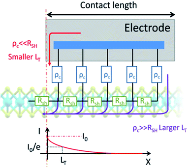 |
| | Fig. 3 Schematic view of current flow across metal/TMD junctions. | |
2.3. Carrier injection at the metal/TMD contact
In the presence of a moderate SB, the main transport mechanism across the metal/TMD interface is thermionic emission, which can be described as| | I = I2D![[thin space (1/6-em)]](https://www.rsc.org/images/entities/char_2009.gif) exp(qV/ηkBT)[1 − exp(−qV/kBT)] exp(qV/ηkBT)[1 − exp(−qV/kBT)] | (1) |
| | 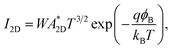 | (2) |
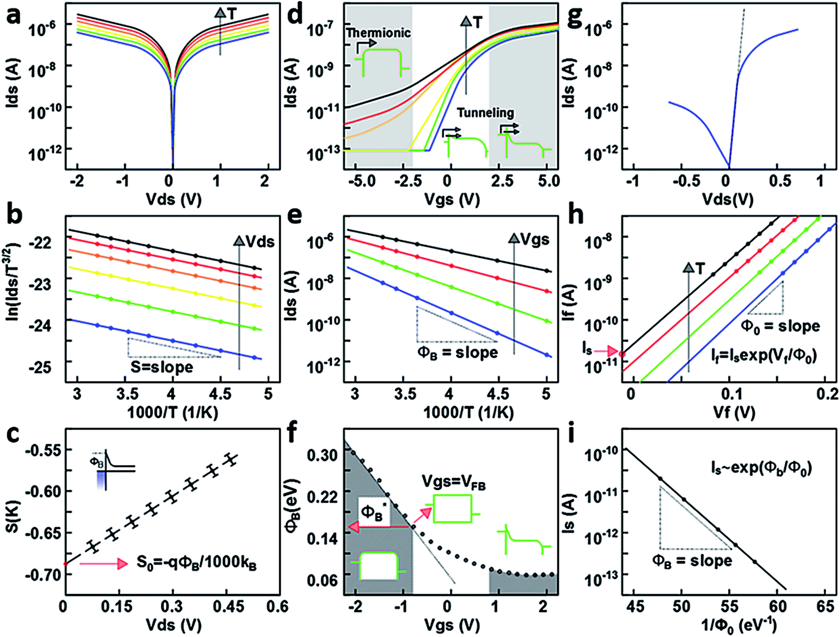
where I2D is the saturation current, W is the junction length, q is the electron charge, ϕB is the SBH, η is the ideality factor, V is the voltage bias, and 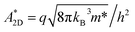 is the 2D equivalent Richardson constant with m* being the electron effective mass (Table 1).24,49,52–54 It is also noteworthy that TMDs exhibit layer dependent effective mass, for instance the effective mass of MoS2 varies from 0.41m0 to 0.57m0 from monolayer to few-layer.55 At sufficient forward bias, the image charge-induced barrier lowering accounted for by the ideality factor can be extrapolated from q/2.3ηkBT = slope of the linear fitting of the semilog I vs. V or log[I/(1 − exp(−qV/kBT))] vs. V plots.54 Meanwhile, at sufficient reverse bias (qV ≫ kBT)
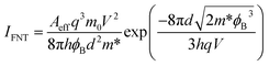
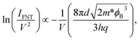
 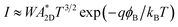 ; therefore, SBH can be calculated from current–temperature measurements as ϕB = (kB/q)(Δln(I/T3/2)/ΔT−1) (Fig. 4a–c).24,35 However, the veracity of the as-extracted SBH should be revised when ϕB < 3kBT or ϕB < 0 because such a SBH is not effective for carrier blocking.31,56,57 Beyond thermionic emission, the applied bias configuration, doping level and temperature can enable direct tunneling (DT; field emission) through a wide-trapezoidal barrier at the quasi-Fermi level and/or thermally assisted Fowler–Nordheim tunneling (FNT; thermionic field emission) through a thin-triangular barrier above the Fermi level but below the top of the SB.58 To discern whether DT or FNT dominates, the ln(I/V2) vs. (I/V) plots should be explored as follows
| | 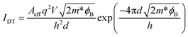 | (3) |
| |  | (4) |
| |  | (5) |
| |  | (6) |
where d is the SB width.59 Accordingly, the SBH can be evaluated by inspecting if the FNT (DT) shows a linear (exponential) trend in the ln(I/V2) vs. (1/V) plot.59,60 In fact, several groups have combined tunneling transport and FLP at the mid-gap to elucidate both the truly SBH, that is the flat band potential (VFB), and the ambipolar behavior.22–24,50,58,61–63 The method assumes thermally activated conduction through the channel as long as Vgs < VFB, that is why the activation energy is linear with Vgs.35,61 Thereby, the linear slope of semilog Idsvs. 1/T plots elucidates the equivalent SB  at different gate bias, and thus VFB can be realized by finding at which Vgs the
  vs. Vgs deviates from linearity (Fig. 4d–f). Alternatively, the thermally assisted tunneling transport can be described as I = Isexp(qV/Φ00), where Is is the saturation current at zero forward voltage and Φ00 is the characteristic energy, both being related as Is ∝ exp(ϕB/Φ00). Accordingly, Is and Φ00 can be extracted from the linear fit of ln(I) vs. V at different temperatures, and ϕB can be extracted by the semi-logarithmic slope of Isvs. 1/Φ00 (Fig. 4g–i).35,64
Table 1 Direct band gap (Eg [eV]), electron effective mass  , dielectric constant (ε [ε0]), natural scaling length (λ [nm]) for 2 nm thick HfO2 (εox = 25), subthreshold slope (SS [mV dec−1]), and drain-induced barrier lowering (DIBL [mV V−1]) of monolayer TMDs.94,95 Reproduced with permission from ref. 94 © 2013, IEEE; ref. 95 © 2014, Applied Physics Letters
| TMD |
E
g [eV] |

|
ε [ε0] |
λ [nm] |
SS [mV dec−1] |
DIBL [mV V−1] |
| MoS2 |
1.8 |
0.56 |
4.8 |
0.41 |
∼60 |
∼10 |
| MoSe2 |
1.51 |
0.62 |
6.9 |
0.49 |
∼65 |
∼15 |
| MoTe2 |
1.10 |
0.64 |
8.0 |
0.54 |
∼70 |
∼20 |
| WS2 |
1.93 |
0.33 |
4.4 |
0.40 |
∼60 |
∼7 |
| WSe2 |
1.62 |
0.35 |
4.5 |
0.42 |
∼63 |
∼10 |
 |
| | Fig. 4 SBH derivation of Co-contacted monolayer MoS2 from (a) the I–V curve, (b) the Arrhenius plot, and (c) the slope (S) extracted from the Arrhenius plot.35 SBH derivation of Ni-contacted 3 nm MoS2 from (d) the transfer characteristics, (e) the Arrhenius plot, and (c) the extracted effective SBH as a function of the gate voltage.23 SBH derivation of graphene-contacted WSe2 from (g) the I–V curve, (h) the temperature dependent If–Vf plot, and (i) the slope extracted from the Isvs. 1/Φ00 plot.64 Reproduced with permission from ref. 35 © 2013, American Chemical Society; ref. 23 © 2012, American Chemical Society; ref. 64 © 2014, American Chemical Society. | |
2.4. Carrier mobility and carrier scattering effects
To investigate the intrinsic charge transport properties of TMDs, it is of paramount importance to properly assess the effective carrier mobility of high quality samples only limited by phonon scattering events. Precise mobility assessment can be done by Hall measurements, the Y-function method, and four-probe or two-probe based transconductance measurements but without RC effects as follows, μFE = (LCg/W)(∂(1/(RT − 2RC))/∂Vgs), where L and W are the channel length and width, respectively.51,65–67 Nevertheless, the presence of Coulomb impurities at the TMD/dielectric interface and defects in low quality samples as well as the substrate roughness affect notoriously the mobility.30 According to Matthiessen's rule, the overall scattered-limited mobility becomes μ(n,T)−1 = μCoulomb(n,T)−1 + μph(T)−1 + μ−1sr where μCoulomb, μph and μsr are the Coulomb scattering, phonon scattering, and surface roughness phonon scattering, respectively.20,25,68 At low temperatures, the mobility is mostly limited by Coulomb scattering arising from ionized impurity charges fixed at the bottom substrate.69 Moreover, the Coulomb scattering is highly intensified in monolayer TMDs due to the short-interaction distance between impurities and carriers. Indeed, an increasing number of layers lead to a higher dielectric constant and charge redistribution far from the interface; as a result, the outer layer experiences reduced Coulomb scattering leading to mobility peaking at ∼10–15 layers.20,25,29,68,70–74 In this regard, experimental results have evidenced Hall mobilities up to 1000 (34000) cm2 V−1 s−1 for 1L (6L) MoS2 at 5 K.25,26,75 At higher temperatures, the electron–phonon interaction becomes dominant, leading to phonon-limited carrier mobility.76,77 The phonon scattering temperature dependence follows the power law μph ∝ T−γ with γ ranging from 0.55 to 1.7 for MoS2 (ref. 27, 75 and 78) and 0.73 to 1.75 for WS2.79 The upper bond mobility limit is determined by the large effective mass and out-of-plane polar phonons (i.e. 410 cm2 V−1 s−1 for 1L MoS2).30,80 Nevertheless, the highest mobilities reported to date at room temperature are 190 (700) cm2 V−1 s−1 for monolayer (10 nm) MoS2,23,81 and ∼250 cm2 V−1 s−1 for monolayer WSe2.82 On the other hand, atomically flat TMDs exhibit negligible surface scattering, in contrast to the severe surface scattering exhibited by 5 nm rough ultrathin Si.30
2.5. Carrier transport and the scattering limited mobility-edge concept
To this extent, the mobility-edge concept, a boundary in the band tail that discriminates between extended and localized states, establishes a useful tool to assess the transport mechanism.28 Extended states enable metallic band-like transport characterized by decreasing mobility with increasing temperature, whereas deep (local) localized states elucidate insulating variable range hopping (thermally activated) transport characterized by increasing mobility with increasing temperature (Fig. 5a). As the gate bias continuously modulates the Fermi energy from localized states to extended states, a metal-to-insulator transition (MIT) can be observed at the threshold carrier concentration.27,83 Below a certain carrier-density limit, the Fermi level lies on deep localized states caused by short-range disorder, leading to electrons flowing by phonon limited thermally activated nearest-neighbor hopping (NNH) conduction at high temperature,84 where kBT1 is the energy spacing between the nearest neighbors, or by weak temperature dependent variable-range hopping (VRH) conduction at low temperature, where T0 is the correlation energy, and d is the material dimensionality (d = 2 for 2D-TMDs).70–72,85–87 However, as the Fermi level moves toward the conduction band localized states are filled and when the Fermi level enters the band-tail carriers become mobile, enabling band-like conduction.71 Alternatively, thermally activated carriers from shallow localized states to the conduction band enable band-like conduction, where Ea is the activation energy.27
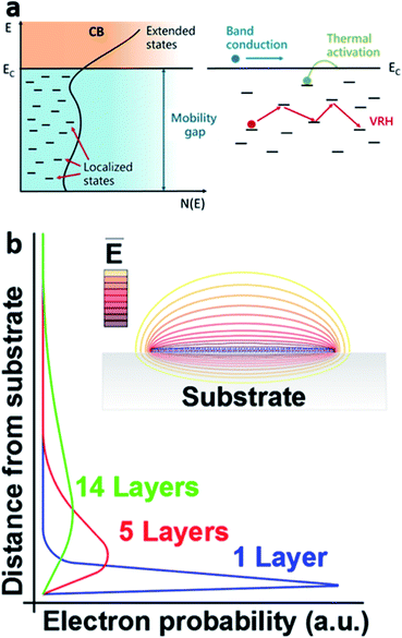 |
| | Fig. 5 (a) Mobility edge concept for carrier transport via hopping (thermal activation) at deep (shallow) localized states or band transport at extended edge states. (b) Carrier distribution in 1, 5, and 14 layer channels.29 Inset: illustration of equipotential electric field lines along the channel.90 Reproduced with permission from ref. 29 and 90 © 2013, American Chemical Society. | |
2.6. Short channel effects and ballistic transport
Typically, the carrier concentration of bulk semiconductors cannot be fully tuned by gate bias because the electric potential is not uniform across the thick bulk semiconductor. In contrast, the dangling-bond free nature and ultrathin structure of 2D-TMDs lead to highly confined carrier distribution close to the gate dielectric and highly uniform potential distribution along the channel, thus allowing homogeneous gating (Fig. 5b).29 Consequently, the drain–source electric field lines fall mostly on the surrounding environment, and thus the semiconductor depletion depth can be replaced by the TMD thickness (tbody) and the semiconductor dielectric constant can be regarded as the environment (Fig. 5b).88–90 The electrostatic integrity can be evaluated by the drain-induced barrier lowering, where low drain-induced barrier lowering (DIBL) yields robustness against short channel effects (SCE).18,28,43,88 Indeed, to suppress SCEs and hence preserve the long channel behavior, the channel length should be at least 4–5 times longer than the electrostatic natural scaling screening length, a figure of merit to distinguish between short and long channel behaviors, where tox and εox are the thickness and dielectric constant of the gate oxide.28,58,73,88,91 Therefore, the rather low screening length enables gate tuning of the carrier concentration n = Cg(Vg − Vth − Vds)/q, where the gate capacitance Cg should include the oxide capacitance (Cox), the TMD quantum capacitance (Cq), and the interface trap density capacitance, where Dit is the trap density.18,28,32,89,92 Nonetheless, in a double-gated geometry Cg should include both top and bottom gate capacitances.25,31,42,65,66,73 Furthermore, as the channel length is scaled down to the electron mean free path, electronic devices are pushed from the diffusion limit to the scattering-free ballistic limit, at which the quantum conductance can potentially reach 2e2/h and the quantum contact resistance can reach 30 Ω μm at a n2D of 1013 cm−2.22,93
To gain further insight on the SCE and ballistic transport characteristics of TMDs, Table 1 shows the λ, SS and DIBL calculated from ballistic transport simulations of scattering-free 15 nm short channels of monolayer TMDs with 2 nm thick HfO2 (εox = 25).94,95 The extremely low λ < 0.5 nm causes a highly intensified electric field at TMD/contact junctions, enabling the possibility to devise tunnel transistors with a high on-current of ∼500 μA μm−1 by engineering the TMD bandgap and effective mass.95 In addition, negative differential resistance (NDR) can be found along ballistic transport due to the narrow energy dispersion of the TMD bands and the reduction of available states in the drain.94,96 Meanwhile, the SS of ∼60 mV dec−1 and DIBL of ∼10 mV V−1 suggest that at the monolayer limit the dielectric environment still dominates the vertical electric field regardless of the TMD dielectric constant.43,94,97 Among the TMDs, the lower electron effective mass and dielectric constant of MoS2, WS2 and WSe2 than those of MoSe2 and MoTe2 lead to the lowest SS and DIBL due to the diminished influence of the drain-triggered lateral electric field.94 Accordingly, the large bandgap and relatively high effective mass of monolayer MoS2 offer a significant on–off ratio, 52% lower DIBL and 13% lower SS than 3 nm Si at 10 nm channel length, and can lead to the DIBL of 100 mV V−1 of ITRS at 8 nm compared to 10 nm Si;97 nevertheless, the lower mobility than most III–V materials makes MoS2 more suited for low standby and operating power than high performance FETs.43 Furthermore, highly scaled p-WSe2 can meet the on-current ITRS requirements for high-performance p-FETs.98 However, monolayer TMDs still offer relatively lower performance than hydrogenated silicene (i.e. silicane).98 On the other hand, the shortest channels experimentally fabricated so far are 10 nm-MoS2/graphene and 7.5 nm 2H/1T MoS2 trenches, which have revealed a SS of 90–120 mV dec−1, an off-current of 10 pA μm−1, and an on–off ratio of 106–107.91,99 Alternatively, ultrashort effective channel lengths developed by top-gated FETs with 10 nm width air-oxidized Al stripes lead to a SS of 80 mV dec−1 with a high on-current of 400 μA μm−1,100 whereas 1 nm carbon nanotube metal gates have led to a SS of 65 mV dec−1 and an on–off ratio of 106.101 Besides MoS2, dual gated BN-encapsulated and graphene-contacted WSe2 with 100 nm local gates has enabled Klein tunneling of Dirac fermions at 20 mK, resembling Fabry–Pérot oscillations and thus suggesting ballistic transport at the local gate.102
3. Carrier injection and carrier transport engineering strategies
We next discuss several engineering strategies to overcome the aforementioned carrier injection and carrier transport limitations toward improving the electronic properties of TMDs. The strategies can be divided roughly into three engineering categories: contact, dielectric and material (Fig. 6a). As low RC is compulsory for efficient carrier transport, we first focus on the contact geometry and how metals and interlayers can further improve RC and different transport aspects. Second, we focus on how surface defects and adsorbates affect the intrinsic electronic properties of the conducting channel, and how the surrounding dielectric passivates scattering centers and tune the electronic transport. Third, we present distinct doping techniques, plasma treatments and phase transformation approaches to tailor the electronic properties of TMDs. To grasp the great throughput of these strategies, Fig. 6b highlights the most remarkable achievements obtained by specific strategies that we detail in the next subsections.
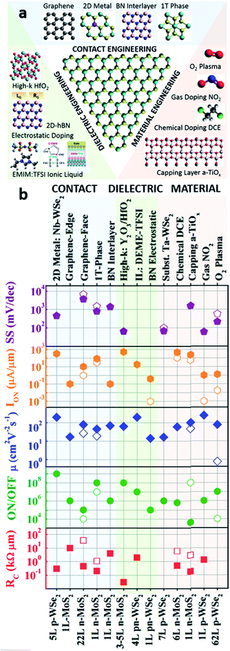 |
| | Fig. 6 (a) Contact, dielectric and material engineering strategies to tune the carrier injection and carrier transport of 2D-TMDs. (b) The most remarkable improved contact resistance and FET characteristics of TMDs to date by engineering strategies; empty and filled symbols indicate before and after applying the strategy, respectively. Contact engineering: Nb–WSe2 2D metal contact,103 graphene-edge and -face contacts,108,124 1T-phase contacts,116 and BN interlayer inclusion.50 Dielectric engineering: stacked high-k Y2O3/HfO2 dielectrics,32 DEME-TFSI ionic liquid,64 and electrostatic doping based on dual gate atomically thin BN (empty symbol: hole, filled symbol: electron).212 Material engineering: Ta-doped p-WSe2via substitutional doping,170 1,2-dichloroethane (DCE) based chemical doping,185 surface charge-transfer via amorphous-titanium suboxide (a-TiOx) capping layer,184 molecular NO2 gas doping,82 and oxygen plasma treatment.191 | |
3.1. Contact geometry engineering
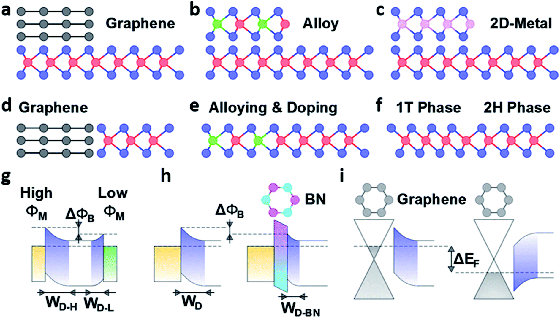
The metal/TMD contact geometry either face-contact or edge-contact also plays a key role in the contact properties.22,37 In the face-contact mode, the direct metal deposition onto TMD fractures covalent bonds and originates defects, enhancing RC due to FLP and high SB. However, transferred metals on 2D-TMDs circumvent the FLP, leading to well-controlled SBs by the Schottky–Mott rule.40 Alternatively, conductive 2D-metals with a wide range of work functions (Fig. 1) offer the possibility to eliminate metal-induced gap states and unbroken covalent bonds by vertically stacking them on 2D-TMDs via vdW forces, thus reducing FLP and enabling tunable SB for both electrons and holes (Fig. 7a–c). For example, thermally stable degenerate Nb0.005W0.995Se2/WSe2 contacts offer an extremely low RC of 300 Ω μm, a world record on–off ratio of 109, an on-current of 320 μA μm−1 and mobilities of 200 and 2000 cm2 V−1 s−2 at 300 K and 5 K respectively.103 Similarly, 2D metallic NbSe2/WSe2 elucidates ohmic contacts from direct tunneling through lowered SB (Fig. 1).104 More interestingly, graphene as a face-contact material can reduce RC dynamically by pumping charge via band alignment modulation.105 On the other hand, edge-contact devised by atomically sharp interfaces strongly reduces the FLP and enables control over the SB.106 To realize edge-contact, several techniques have been formulated as follows (Fig. 7d–f). (i) BN-sandwiched TMDs provide 1D atomic edge ohmic contacts with superior mobility and stability.26,50 (ii) Aromatic molecule-assisted in-plane atomic stitching enables large-scale graphene/MoS2 with a RC of 300 Ω μm.107 (iii) Epitaxial growth of lateral graphene/MoS2, graphene/WSe2 and graphene/WS2 heterostructures results in RC as low as 11 kΩ μm, 50 kΩ μm and 30 kΩ μm, respectively.108–110 (iv) Degenerate edge contacts by alloying (i.e. WxNb1−xSe2/WSe2) or chemical doping (i.e. NO2-doped p+ WSe2, K-doped n+ WSe2, and P-doped p+-MoS2) lead to low interface-trap density ohmic contacts.82,111–113 (v) 2D-TMD lateral heterojunctions.114,115 (vi) Phase transformation yields low SB due to the close band alignment between the metallic-phase work function and the semiconducting-phase conduction band, enabling RC as low as 200 Ω μm.116 (vii) Semiconducting to metallic/semimetallic transitions from monolayer to multilayer in noble-TMDs such as PtSe2 and PdS2 owing to the strong interlayer bonding allow the fabrication of single-material nanoelectronic devices with low leakage current and extremely low contact resistance down to 70 Ω μm.117–119
 |
| | Fig. 7 Contact geometry strategies to improve 2D-TMD contacts. Face contacts: (a) graphene, (b) alloy, and (c) 2D metal. Edge contacts: (d) graphene, (e) alloying and doping, and (f) 2H to 1T phase transformation. Illustration of 2D-TMD/metal contact strategies to tune the SB and depletion width. (g) High versus low metal work function, (h) ultra-thin interfacial layers such as boron nitride (BN), and (i) gate-tunable graphene Fermi level. | |
3.2. Metal contact engineering
The dangling bond-free nature and ultra-thin structure of 2D TMDs do not lead to the formation of any chemical bond with metals; however, the native defects of TMDs induce Fermi level shifts of 1 eV over nanometer scale areas regardless of the metal contact work function (Fig. 1), providing low SBs that in turn reduce RC and boost the on-current via band-tunneling while preserving the SS value.120,121 Moreover, metal-induced doping via narrow bandgap or metallic surface state formation can also shift the Fermi level, and thus alleviate the interfacial barrier.41 For example, Al (Ag) onto monolayer WSe2 greatly (slightly) shifts the Fermi level toward the conduction band, indicating weak (strong) electron doping characteristics due to the low (high) density of states of Al (Ag) near the WSe2 Fermi level.122 Therefore, the prospective choice of metals with the optimal work function can engineer ohmic contacts with negligible RC. For instance, In and Ag metals having a work function close to the electron affinity of WSe2 form low resistant n-type ohmic contacts with ambipolar WSe2, leading to an on-current of 210 μA μm−1.122 Similarly, Sc or Ti (Pt) metals with a low (high) work function of 3.5 or 4.3 eV (5.9 eV) contacting multilayer MoS2 can form ohmic (Schottky) contacts; as a consequence, the Sc-ohmic contact affords highly effective mobilities of 700 cm2 V−1 s−1 (Fig. 7g).23 More interestingly, Pd-contacted few-layer MoS2 results in p-type doping, leading to the photovoltaic effect by contacting the other side with Au.123 Nevertheless, transferred Ag (Pt) electrodes on MoS2 that avoid the FLP effect lead to 20 (67) meV electron (hole) SBs, enabling 260 (175) cm2 V−1 s−1 electron (hole) mobilities and 0.66 (0.21) mA μm−1 on-current.40 However, the Fermi level of bulk metals is fixed due to the vast sea of electron concentrations, and thus it is not tunable by electrostatic gating. Conversely, graphene offers not only a gate-tunable Fermi level but also an interfacial layer to avoid metal-induced damage, leading to an extremely low RC of 200 Ω μm (Fig. 7i).64,124 Furthermore, vacuum annealing engineering is a proven tool to improve RC.125 For example, varying from ultra-high vacuum (10−9 Torr) to high vacuum (10−6 Torr) during Au, Cr, Ir, Sc metal deposition strongly influences RC due to the chemical nature of the interface (i.e., covalent bonds, vdW gaps, or permalloys).126,127
3.3. Metal/TMD interface engineering
Interface engineering is a promising strategy to modulate the metal/TMD SB. As striking consequences, the RC can be highly reduced via FLP annihilation, and the channel can be populated with both electrons and holes toward ambipolar conduction. In fact, DFT calculations predict that 0.6 nm vdW-gaps can precisely tune the metal work function-dependent SB.38 Furthermore, electrons tunneling through dangling bond-free ultrathin boron nitride (BN) interlayers can annihilate the FLP and enable SB tunability while preserving the intrinsic MoS2 band structure, thus leading to reversible gate tunable ambipolar p–n junctions (Fig. 7h).39,50,128 Alternatively, metal oxides provide a fruitful path to unpin the Fermi level. For example, high work function metal Pd/MoOx/MoS2 contacts or the Co catalytic oxidation of multilayer MoS2 into MoOx nanoparticles can enable ambipolar transport owing to efficient hole injection into MoS2; consequently asymmetric Ni/MoS2/MoOx/Pd diodes show a rectification ratio of 105 and an ideality factor of 1.4.129,130 Furthermore, the insertion of TiO2 or MgO thin films between a ferromagnetic Co electrode and MoS2 significantly lowers the SB toward efficient spin tunnel contacts, leading to a 100-fold on–off ratio and 7-fold mobility enhancements.35,63 Similarly, 2 nm ultrathin TiO2 or Al2O3 interlayers can unpin Ti, Ni, Au and Pd metals from MoS2, and thus reduce the SB by shifting the Fermi level toward the conduction band; consequently, LT substantial reduces to 280 nm, inducing 5–24 fold RC reduction as well as 10-fold mobility and 5-fold on-current enhancements.131,132 A more subtle technique to reversibly modulate the contact resistance by 4 orders of magnitude is by exerting vertical compression via the tip force of a conductive atomic force microscope owing to the enhanced quantum tunneling.133 For instance, depending on the compressive load applied on a MoS2/graphene system a small band gap up to 12 meV can be induced within the band structure, thus significantly reducing the SBH and increasing the electron density which improve the current injection.134
3.4. TMD surface engineering
The high surface-to-volume ratio and ultra-thin structure of TMDs make their intrinsic physical and chemical properties highly sensitive to perturbations in the lattice structure, similar to low-dimensionality oxide nanostructures.135–137 Particularly, the TMD work function governs the band bending at the metal/TMD interface and hence the charge transport. The MoS2 work function highly varies with distinct atmospheric conditions (4.36 eV for ambient, 4.04 eV for UHV and 4.47 eV for O2), indicating that adsorbents are strong enough to modulate the electronic energy levels in MoS2; consequently, the charge transport under ambient, low vacuum, and high vacuum conditions is dominated by thermionic, thermionic-tunneling, and tunneling transport, respectively.138 In fact, physisorption and chemisorption of both water and oxygen have been reported to deplete electrons in n-type TMDs, thus inducing p-doping and weakening the electrostatic screening; conversely, holes are accumulated in p-type TMDs, leading to stronger p-type behavior.139,140 Consequently, the on-current of MoS2 degrades by two orders of magnitude, suggesting that the adsorption of gas molecules at surface defects is an efficient molecular gating strategy with superior control over the charge density than electrostatic gating. Nonetheless, the device performance can be recovered by desorbing adsorbates via vacuum annealing.79,140 However, there is some discrepancy regarding the oxygen adsorption on MoS2. For instance, Qi et al. pointed out that after diminishing the effect of physically adsorbed oxygen molecules almost to zero by using a UHV system with a well-controlled oxygen partial pressure, solely the effect of oxygen chemisorption on surface defects of few layer MoS2 results in n-doping without mobility degradation owing to the dissociative adsorption of oxygen, which lowers the conduction band edge locally.141 Furthermore, Komsa et al. deliberately created sulfur vacancies on monolayer MoS2 by electron-beam irradiation and studied whether they could be filled by oxygen and other species to induce doping; as a consequence they showed that substitutional oxygen at sulfur vacancies does not produce any localized state in the gap region, whereas N, P, As and Sb behave as acceptors and F, Cl, Br, and I behave as donors.142 Alternatively, Mahdi et al. showed that the combination of angle-dependent and ion-type beam-irradiation and post-exposure to precursors gases could be used to induce doping as well, and thus tune the electronic properties towards for example negative differential resistance.143
3.5. Solid state dielectric engineering
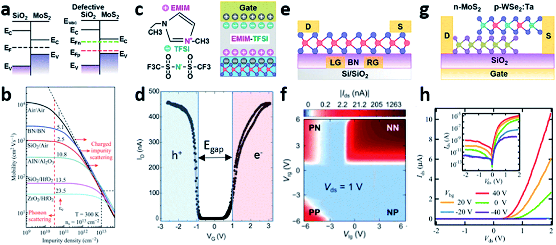
Typically, gate dielectrics are responsible for slow and fast charged traps that lead to severe reliability issues such as hysteresis and temperature instabilities, respectively. In this regard, pristine-BN substrates mitigate hysteresis via slow trap suppression but deteriorate the temperature dependence due to thermally activated traps.144 Moreover, localized states owing to defective gate dielectrics have been regarded as the origin of the ambipolar conductivity of MoS2 (Fig. 8a).145 Interestingly, multilayer MoS2 on PMMA (SiO2) exhibits ambipolar (unipolar) transport with high (low) mobilities, suggesting that long (short) range disorder dominates PMMA (SiO2) dielectrics.146 On the other hand, high-k gate dielectrics such as HfO2, ZrO2, and Al2O3 allow not only broad carrier density modulation (∼1010–1013 cm−2) to enable band-transport, but also high carrier mobility enhancement due to the suppression of Coulomb scattering and optical phonon modes (Fig. 8b); for instance 10 nm Al2O3 (30 nm HfO2) top gated 23L (1L) n-MoS2 achieves a remarkable mobility of 517 (217) cm2 V−1 s−1 with an on–off ratio of 108.10,25,29,69,147,148 However, the high dissociative activation energy between HfO2 and MoS2 leads to substantial leakage current; as a solution, buffer layers such as Mg, Al2O3, Y2O3 improve the conformability between HfO2 and MoS2. Accordingly, Y2O3/HfO2 stacks exhibit high-quality interfaces with a low Dit of ∼2 × 1012 cm−2 eV−1, thus yielding a SS of 65 mV dec−1 and a saturation on-current of 526 μA μm−1.32 An alternative to high-k dielectrics is atomically flat BN with a relative permittivity of 3.5 (close to 3.9 of SiO2) enabling room temperature mobilities of 140, 214, 151 cm2 V−1 s−1 with on–off ratios of 106 to 107 in 3L p-WSe2, 1L n-WS2, and 1L n-MoS2, respectively.149–151
 |
| | Fig. 8 Dielectric engineering: (a) schematic of the MoS2 band diagram on defective SiO2 with either donor (green line) or acceptor (red line) states, showing the n- or p-type conduction modulation,145 and (b) the net electron mobility at room temperature of monolayer MoS2 surrounded by different dielectrics and considering different scattering mechanisms.69 Ionic gating: (c) schematic of the EMIM-TFSI ionic liquid and ionic gate effect, and (d) ionic gate transfer characteristics of WSe2 indicating the bandgap estimation from the ambipolar transport.157 Electrostatic doping: (e) device schematic of the left and right gate (LG, and RG) configuration, and (f) color maps of the left and right gate transfer characteristics of WSe2 highlighting the PP, NN, NP, and PN behaviors.164 Substitutional doping: (g) schematic of a p-WSe2:Ta/n-MoS2 heterostructure, and (h) the gate tunable rectifying characteristics.170 Reproduced with permission from ref. 145 © 2013, American Physical Society; ref. 69 © 2014, American Physical Society; ref. 157 © 2012, American Chemical Society; ref. 164 © 2014, American Chemical Society; ref. 170 © 2017, American Institute of Physics. | |
3.6. Ionic liquid and polymer electrolyte engineering
Ionic liquids (ILs) and polymer electrolytes (PE) are cationic–anionic binary organic salts and polymers that under positive (negative) gate bias can accumulate negative (positive) and positive (negative) charge on the gate or TMD channel, respectively (Fig. 8c).152–154 Consequently, ultrathin (∼1 nm) spatial charge doublets form at the interface, leading to electric double layers (EDLs) that mimic nanogap capacitors with extremely high capacitance (∼100 μF cm−2).152,155 The strong gate-channel coupling in combination with solid state back gates allows fine Fermi level tuning across the whole bandgap, and thus makes it possible to access quasi-continuously a large range of carrier densities up to 1014 cm−2.152,153,155,156 Such fine carrier density tuning capability enables the investigation of novel intriguing properties and phenomena, as we next enumerate. (i) Charge transfer between the electrolyte and TMD takes place until the electrolyte redox potential aligns with the TMD Fermi level; consequently, the band bending induced by the space charge reduces the contact barrier and facilitates tunneling carrier injection, boosting the mobility and reducing the subthreshold slope down to 62 mV dec−1.152,155,157,158 (ii) Ambipolar transport has enabled the possibility to find holes with higher mobility than electrons in MoS2 as well as to quantitatively determine the band gap based on the electron–hole threshold voltage difference (Fig. 8d).157,159,160 (iii) Ambipolar transistors operating beyond the electron saturation regime, where electrons and holes are injected from opposite contacts, have been used to devise stable pn junctions at temperatures below the glass transition temperature that emit either unpolarized or Zeeman-type circularly polarized light.159–162 (iv) Gate-induced MIT transitions followed by superconductivity with enhanced transition temperature.155,156
3.7. Doping engineering
Doping is the most universal technique to control the carrier type and carrier concentration in the semiconductor industry and thus enable versatile electronic devices. Nevertheless, the conventional techniques used to dope bulk semiconductors (i.e. Si or GaAs) such as dopant diffusion or ion-implantation are not suitable for novel 2D materials such as layered TMDs due to the induced damage. Consequently, alternative doping strategies are required. Therefore, we next review the most successful engineering strategies to precisely control the doping level.
3.7.1. Electrostatic doping.
Electrostatic doping, characterized by external perpendicular electric field-induced charge transfer, can tune the electrical transport without introducing disorder and causing defects. Moreover, the charge transfer is reversible and offers long-term stability. In this regard, the 2D nature and weak dielectric screening characteristics of TMDs enable improved electrostatic control than those of 3D materials to finely tune the Fermi level across the electronic bandgap.58 Therefore, symmetric dual local gate structures shed light to tailor the depletion width at the source and drain contacts independently, and thus reconfigure TMDs from metallic isotype (p–p, n–n) to rectifying anisotype (p–n and n–p) behaviors toward multifunctional devices (Fig. 8e and f).163–167 Additionally, owing to the thickness dependence of TMDs, the gate bias effect on LT must be carefully addressed to avoid detrimental impact on RC prospects.46,47,132
3.7.2. Substitutional doping.
Substitutional doping, characterized by replacement of host atoms by dopant atoms, is one of the most common strategies. In this regard, controlled soft phosphor plasma can induce a broad range of p-type doping in MoS2 with minimum surface damage, and thus form high quality pn junctions with unexposed n-MoS2.113 Alternatively, adjusting the molar ratio of source materials or intercalating metal/dopant/metal stacks during chemical vapor growth could yield specific doping ratios of the desired crystals.168,169 On this point, Nb with a similar ionic radius and oxidation state to Mo, only one valence electron less than Mo, is a perfect acceptor candidate for either MoS2 or MoSe2; therefore, Nb–MoS2 has enabled different degrees of p-type doping from degenerate for ohmic contacts to non-degenerate for pn junctions and ambipolar FETs.168,169 Similarly, Ta matches the ionic radius and oxidation state of W, leading to excellent p-type behavior; thereby, p-Ta0.01W0.99Se2/n-MoS2 yields an impressive rectification ratio of 105 with an ideality factor of 1 (Fig. 8g and h).170
3.7.3. Chemical doping.
Molecular absorption-induced chemical doping is a high-throughput tool that can modulate the carrier concentration and shift the Fermi level of the host material via surface charge-transfer while preserving the electronic properties without inducing defects. Considering that the electronegativity (χ) measures the electron attraction tendency of a medium, the surface charge-transfer process between two media can be understood by the electronegativity differences, which determine the net charge flow direction and thus which medium becomes the electron donor or acceptor. Therefore, the higher electronegativity medium withdraws electrons from the other, and the larger the electronegativity difference, the larger the amount of transferred electrons. The dopant molecule electronegativity is defined as χmol = 1/2(IP + EA), where IP is the first ionization potential (the energy to withdraw an electron and form a cation, which is equal to the negative of the highest occupied molecular orbital (HOMO)), and EA is the electron affinity (the energy needed to withdraw an electron from an anion, which is equal to the negative of the lowest unoccupied molecular orbital (LUMO)).171 On the other hand, the TMD electronegativity χTMD = EVBM + Ee − 0.5Eg, where EVBM is the valence band maximum (VBM) potential against the normal hydrogen electrode (NHE), Ee (∼4.5 eV) is the free electron energy on the hydrogen scale (i.e. the standard electrode potential on the NHE scale), and Eg is the bandgap. In this regard, Fig. 1 shows the band alignment of monolayer TMDs and the water reduction (H+/H2) and oxidation (H2O/O2) potential with respect to the vacuum level.172 It is noteworthy that the concomitant formation of large surface dipoles between charged dopant ions and oppositely charged TMDs alters the vacuum level across the interface, contributing additionally to the work function modulation (Fig. 9a).173
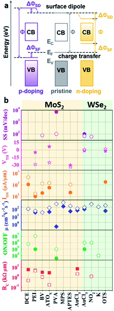 |
| | Fig. 9 (a) Schematic of the doping effect on the work function change (Δϕ/) by emptying/filling states (ΔϕSF) and creating surface dipoles (Δϕ/SD).173 (b) Electronic properties of MoS2, and WSe2 before (filled symbols) and after (empty symbols) chemical doping by different dopants: dichloroethane (DCE),67 polyethyleneimine (PEI),181 benzyl viologen (BV),186 amorphous-TiO2−x (ATOx),184 polyvinyl alcohol (PVA),213 (3-mercaptopropyl)trimethoxysilane (MPS),25 aminopropyltriethoxysilane (APTES),214 gold chloride (AuCl3),78,158 (NO2),82 potassium (K),215 and octadecyltrichlorosilane (OTS).214 Reproduced with permission from ref. 173 © 2017, American Chemical Society. | |
Therefore, dopant molecules with a higher (lower) electronegativity/reduction potential than the flat band potential of n-type TMDs work as electron donors (acceptors) by donating (withdrawing) electrons to (from) the n-type TMD, which increases (decreases) the TMD electron carrier concentration; conversely, molecules with higher (lower) electronegativity than p-type TMDs withdraw (donate) electrons from (to) the p-type TMD, which depletes (accumulates) holes and thus decreases (increases) its hole carrier concentration. Fig. 9b summarizes several reductant (oxidant) agents enabling n-type (p-type) doping in TMDs.20,139,174–183 For example, amorphous-TiO2−x (chloride) doping significantly reduces the RC and LT of MoS2 down to 180 (500) Ω μm and 15 (60) nm, respectively, which is one of the lowest RC values reported to date, as a consequence of the substantial SB thinning induced by the heavy doping nearby the contact region.67,184,185 Meanwhile, NO2 chemisorption leads to degenerate p+-WSe2, thus enabling hole tunneling injection into p-WSe2 through a narrower SB which enables ohmic contacts for the inspection of a high hole mobility of 250 cm2 V−1 s−1, a SS of 60 mV dec−1 and an enhanced on–off ratio.82 Benzyl viologen can degenerate MoS2 in the proximity of the metal contacts, leading to 3-fold RC reduction and a SS of 77 mV dec−1.186 Furthermore, Au nanoparticle (NPs) decoration via AuCl3 reduction on either n-MoS2 or p-WSe2 have shown p-type doping owing to the electron transfer from TMDs to high work function Au.78,158,187,188 Indeed, increasing the AuCl3 dopant concentration from 5 M to 20 M yields degenerate p-type doping in MoS2, which has been used to devise CMOS inverters or nearly ideal rectifying pn diodes.78,188
3.8. Plasma engineering
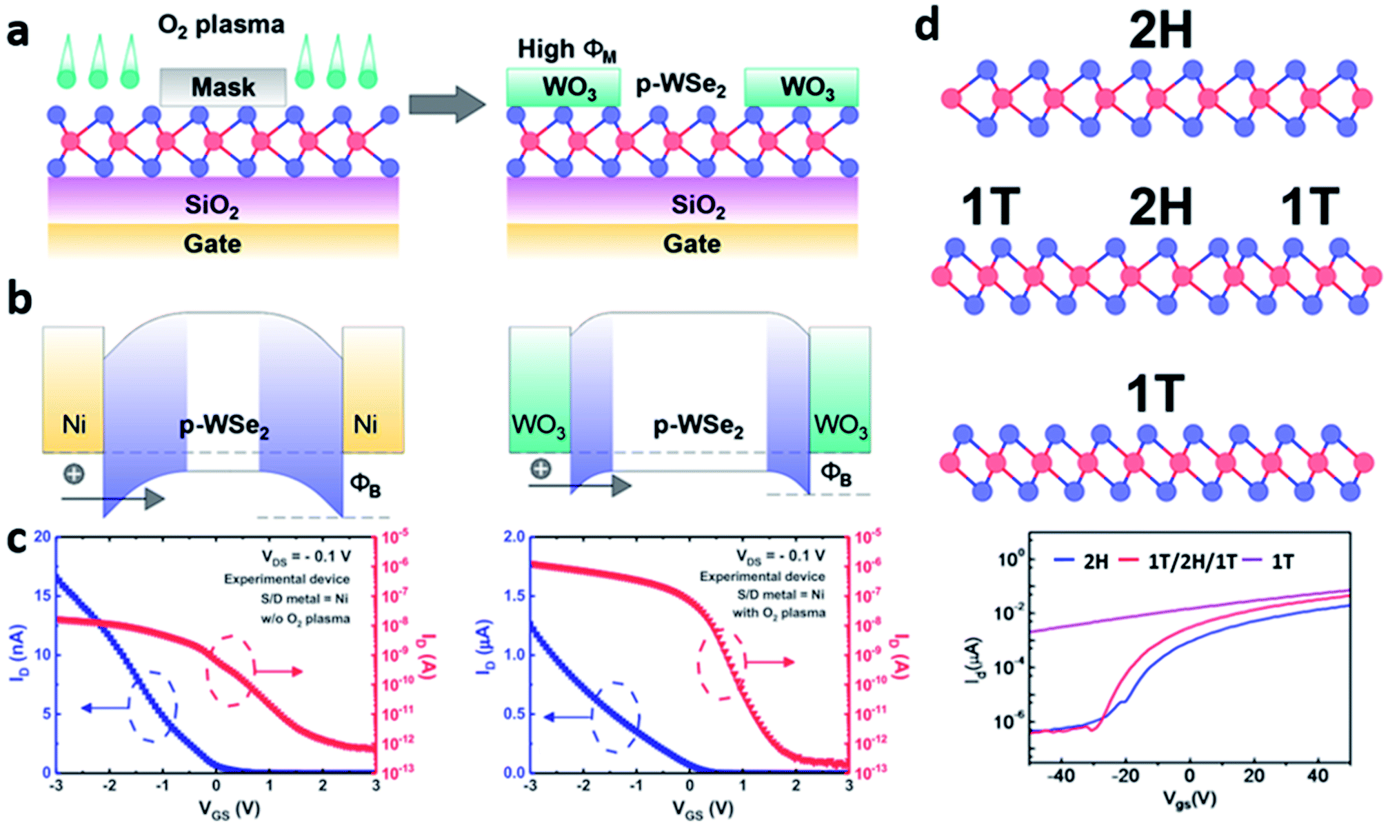
Plasma treatment is a versatile tool to control the electronic properties of TMDs. For example, O2 plasma exposure oxidizes MoS2 by knocking off sulfur atoms and creating defects, thus leading to MoO3. The higher work function of MoO3 (6.9 eV) than MoS2 (4.9 eV) creates a band offset between them; consequently, the interface between the exposed channel and the unexposed contacts forms a SB that acts as a tunneling barrier for electron injection.189,190 Similarly, the O2 plasma oxidizes p-WSe2 into high work function WO3 (6.7 eV), which improves the hole injection via SBH lowering, and thus reduces RC and enhances mobility (Fig. 10a–c).191 On the same line, selective contact area O2 or Ar plasma exposure broadens the SBH distribution from 0.2–0.3 to 0.2–0.8 eV of MoS2, thus degrading the electron mobility but enabling hole injection toward ambipolar transport.192 Conversely, soft O2, Ar, UV/ozone plasma treatments can repair structural defects, remove contaminants and passivate photo-excited traps, respectively, leading to enhanced mobility.193–195 Alternatively, the H2 plasma promotes the formation of sulfur vacancies, which act as a double-edged sword because they reduce contact resistance but at the same time increase the number of scattering centers that eventually reduce the mobility.196 Additionally, contact-defect engineering by H2 plasma treatment leads to air-stable degenerate n-WSe2 with 2 orders of magnitude lower RC compared to the pristine sample; consequently the on-current increases 20-fold and the SS reduces down to 66 mV dec−1.197
 |
| | Fig. 10 Oxygen plasma exposure of WSe2: (a) schematic showing the formation of WO3 after O2 plasma exposure, (b) improved hole injection via SB reduction due to the formation of high work function WO3, and (c) transfer characteristics before and after oxygen plasma treatment.191 (d) Schematic of devices based on the 2H to 1T phase transformation of MoS2 by argon plasma and the corresponding transfer characteristics.201 Reproduced with permission from ref. 191 © 2017, Elsevier; ref. 201 © 2017, American Chemical Society. | |
3.9. Phase transformation engineering
Beyond the conventional 2H-semiconducting phase of TMD materials, there exist several polymorphic phases with intriguing states of matter such as 2D topological insulators, superconductors and Weyl semimetals.198–200 Among them, the metallic phase characterized by V-shaped Dirac-Fermion like carriers, carrier concentrations higher than 1013 cm−2, weak gate modulation and environmental stability can resolve the Schottky-limited transport in 2D-TMDs.201 For instance, seven monolayer 1T-metallic phase TMD/metal structures have been theoretically identified by Ouyang et al. as zero Schottky barrier contacts owing to efficient interface charge transfer based on the amount of interface orbital overlapping and lattice misfit.202 Indeed, selective area semiconducting-to-metallic phase transformation exhibits defect-free atomically sharp interfaces and matched band alignment between the work function and the conduction band energy, leading to seamlessly ohmic side contacts with RC as low as 200–300 Ω μm as well as improved device characteristics (Fig. 10d).52,91,116,201,203,204 In addition, the metallic-1T phases of MoS2, MoTe2 and WSe2 are stable up to 100, 300 and 180 °C respectively, although further thermal annealing or laser irradiation can reverse the transition back to the 2H-semiconducting phase.203,205,206 Furthermore, experimental and theoretical calculations of sub-10 nm 1T/2H/1T MoS2 structures exhibit an off-current of 10 pA μm−1, an on–off ratio of 104–107, and a SS of 69–120 mV dec−1, which are only limited by intraband tunneling at 3.3 nm.91,207
4. Conclusion, outlook and perspectives
This review summarizes the impact of the compelling properties of 2D-TMDs including chemical inertness, atomically thin nature, low DOS and large bandgaps on the carrier injection and transport towards high performance electronic devices. Although, the weak screening in 2D-TMDs enables fine carrier density modulation up to 1014 cm−2, allowing metal-to-insulator transitions with optimized superconducting temperature, we emphasis that utmost care should be taken first on addressing the RC, SB and FLP in order to achieve carrier injection with ohmic-contacts, and second on suppressing carrier traps and phonon scattering centers in order to achieve high mobility carrier transport towards ballistic transport in highly scaled devices.
To this extent, we survey several contact, dielectric and material engineering strategies involving surface and interface chemistry to optimize the charge injection and transport. The most successful strategies optimizing charge injection include graphene and BN 2D-interlayers, coplanar 2H-semiconducting/1T-metallic phase transitions, 1L-semiconducting/2L-metallic transitions in PtSe2, and amorphous TiOx capping layers; consequently, RC can be reduced down to 300–70 Ω μm, which is in close proximity to the 100 Ω μm speculated by the ITRS roadmap. Furthermore, metal-transferred electrodes and alloyed 2D-metals not only provide low RC ohmic contacts but also afford mobilities of 200–260 cm2 V−1 s−1 and on-currents of 320–660 μA μm−1. On the other hand, the current transport can be readily tailored from degenerate doping to ambipolar transport by charge transfer via thiol-based self-assembled monolayers, AuCl3 or potassium chemical doping, NO2 gas exposure, and phosphor plasma among others. Furthermore, few-layer BN and Y2O3/HfO2 stacked gate dielectrics can suppress phonon scattering and boost the mobility over 200 cm2 V−1 s−1 at RT, whereas, ionic electrolytes induce lowered SB via strong surface band bending, hence enabling tunneling currents that provide subthreshold swing slopes down to 60 mV dec−1. Therefore, the remaining challenge for the next-generation of high performance electronic devices based on the unique properties of 2D-TMDs is to integrate the aforementioned strategies into large-scale and high-quality samples grown by either chemical-vapor-deposition techniques208,209 or alternatively by solution processing methods,210,211 which is certainly coming soon, but is not yet fully established.
Conflicts of interest
There are no conflicts to declare.
Acknowledgements
This work was financially supported by the King Abdullah University of Science and Technology (KAUST) Office of Sponsored Research (OSR-2016-CRG5-3005), KAUST Sensor Initiative, KAUST Solar Center, and KAUST baseline funding.
References
- A. M. Ionescu and H. Riel, Nature, 2011, 479, 329–337 CrossRef CAS PubMed.
- Y. Khatami and K. Banerjee, IEEE Trans. Electron Devices, 2009, 56, 2752–2761 CAS.
- Z. Qin, Z. Wei and A. Seabaugh, IEEE Electron Device Lett., 2006, 27, 297–300 Search PubMed.
- H. Lu and A. Seabaugh, IEEE J. Electron Devices Soc., 2014, 2, 44–49 CAS.
- M. Si, C.-J. Su, C. Jiang, N. J. Conrad, H. Zhou, K. D. Maize, G. Qiu, C.-T. Wu, A. Shakouri, M. A. Alam and P. D. Ye, Nat. Nanotechnol., 2018, 13, 24–28 CrossRef CAS PubMed.
- F. A. McGuire, Z. Cheng, K. Price and A. D. Franklin, Appl. Phys. Lett., 2016, 109, 093101 CrossRef.
- K. F. Mak, C. Lee, J. Hone, J. Shan and T. F. Heinz, Phys. Rev. Lett., 2010, 105, 136805 CrossRef PubMed.
- K. S. Novoselov, D. Jiang, F. Schedin, T. J. Booth, V. V. Khotkevich, S. V. Morozov and A. K. Geim, Proc. Natl. Acad. Sci. U. S. A., 2005, 102, 10451–10453 CrossRef CAS PubMed.
- D. Lembke, S. Bertolazzi and A. Kis, Acc. Chem. Res., 2015, 48, 100–110 CrossRef CAS PubMed.
- B. Radisavljevic, A. Radenovic, J. Brivio, V. Giacometti and A. Kis, Nat. Nanotechnol., 2011, 6, 147–150 CrossRef CAS PubMed.
- A. K. Geim and I. V. Grigorieva, Nature, 2013, 499, 419–425 CrossRef CAS PubMed.
- M. Chhowalla, H. S. Shin, G. Eda, L.-J. Li, K. P. Loh and H. Zhang, Nat. Chem., 2013, 5, 263 CrossRef PubMed.
- A. H. Castro Neto, Phys. Rev. Lett., 2001, 86, 4382–4385 CrossRef CAS PubMed.
- H. Li, J. Wu, Z. Yin and H. Zhang, Acc. Chem. Res., 2014, 47, 1067–1075 CrossRef CAS PubMed.
- S. Mao, J. Chang, H. Pu, G. Lu, Q. He, H. Zhang and J. Chen, Chem. Soc. Rev., 2017, 46, 6872–6904 RSC.
- R. Lv, J. A. Robinson, R. E. Schaak, D. Sun, Y. Sun, T. E. Mallouk and M. Terrones, Acc. Chem. Res., 2015, 48, 56–64 CrossRef CAS PubMed.
- D. Jariwala, V. K. Sangwan, L. J. Lauhon, T. J. Marks and M. C. Hersam, ACS Nano, 2014, 8, 1102–1120 CrossRef CAS PubMed.
- H. Ilatikhameneh, Y. Tan, B. Novakovic, G. Klimeck, R. Rahman and J. Appenzeller, IEEE Journal on Exploratory Solid-State Computational Devices and Circuits, 2015, 1, 12–18 Search PubMed.
- D. Sarkar, X. Xie, W. Liu, W. Cao, J. Kang, Y. Gong, S. Kraemer, P. M. Ajayan and K. Banerjee, Nature, 2015, 526, 91–95 CrossRef CAS PubMed.
- H. Schmidt, F. Giustiniano and G. Eda, Chem. Soc. Rev., 2015, 44, 7715–7736 RSC.
- Q. H. Wang, K. Kalantar-Zadeh, A. Kis, J. N. Coleman and M. S. Strano, Nat. Nanotechnol., 2012, 7, 699 CrossRef CAS PubMed.
- A. Allain, J. Kang, K. Banerjee and A. Kis, Nat. Mater., 2015, 14, 1195–1205 CrossRef CAS PubMed.
- S. Das, H. Y. Chen, A. V. Penumatcha and J. Appenzeller, Nano Lett., 2013, 13, 100–105 CrossRef CAS PubMed.
- C. Kim, I. Moon, D. Lee, M. S. Choi, F. Ahmed, S. Nam, Y. Cho, H. J. Shin, S. Park and W. J. Yoo, ACS Nano, 2017, 11, 1588–1596 CrossRef CAS PubMed.
- Z. Yu, Y. Pan, Y. Shen, Z. Wang, Z. Y. Ong, T. Xu, R. Xin, L. Pan, B. Wang, L. Sun, J. Wang, G. Zhang, Y. W. Zhang, Y. Shi and X. Wang, Nat. Commun., 2014, 5, 5290 CrossRef CAS PubMed.
- X. Cui, G. H. Lee, Y. D. Kim, G. Arefe, P. Y. Huang, C. H. Lee, D. A. Chenet, X. Zhang, L. Wang, F. Ye, F. Pizzocchero, B. S. Jessen, K. Watanabe, T. Taniguchi, D. A. Muller, T. Low, P. Kim and J. Hone, Nat. Nanotechnol., 2015, 10, 534–540 CrossRef CAS PubMed.
- B. Radisavljevic and A. Kis, Nat. Mater., 2013, 12, 815–820 CrossRef CAS PubMed.
- W. Zhu, T. Low, Y. H. Lee, H. Wang, D. B. Farmer, J. Kong, F. Xia and P. Avouris, Nat. Commun., 2014, 5, 3087 CrossRef PubMed.
- S.-L. Li, K. Wakabayashi, Y. Xu, S. Nakaharai, K. Komatsu, W.-W. Li, Y.-F. Lin, A. Aparecido-Ferreira and K. Tsukagoshi, Nano Lett., 2013, 13, 3546–3552 CrossRef CAS PubMed.
- Z. Yu, Z. Y. Ong, Y. Pan, Y. Cui, R. Xin, Y. Shi, B. Wang, Y. Wu, T. Chen, Y. W. Zhang, G. Zhang and X. Wang, Adv. Mater., 2016, 28, 547–552 CrossRef CAS PubMed.
- S.-L. Li, K. Tsukagoshi, E. Orgiu and P. Samori, Chem. Soc. Rev., 2016, 45, 118–151 RSC.
- X. Zou, J. Wang, C. H. Chiu, Y. Wu, X. Xiao, C. Jiang, W. W. Wu, L. Mai, T. Chen, J. Li, J. C. Ho and L. Liao, Adv. Mater., 2014, 26, 6255–6261 CrossRef CAS PubMed.
- Y. Liu, P. Stradins and S.-H. Wei, Sci. Adv., 2016, 2(4), e1600069 Search PubMed.
- Y. Guo, D. Liu and J. Robertson, Appl. Phys. Lett., 2015, 106, 173106 CrossRef.
- J. R. Chen, P. M. Odenthal, A. G. Swartz, G. C. Floyd, H. Wen, K. Y. Luo and R. K. Kawakami, Nano Lett., 2013, 13, 3106–3110 CrossRef CAS PubMed.
- P. Dharmaraj, P. J. Jesuraj and K. Jeganathan, Appl. Phys. Lett., 2016, 108, 051605 CrossRef.
- J. Kang, W. Liu, D. Sarkar, D. Jena and K. Banerjee, Phys. Rev. X, 2014, 4, 031005 Search PubMed.
- C. Gong, L. Colombo, R.
M. Wallace and K. Cho, Nano Lett., 2014, 14, 1714–1720 CrossRef CAS PubMed.
- M. Farmanbar and G. Brocks, Phys. Rev. B: Condens. Matter Mater. Phys., 2015, 91, 161304(R) CrossRef.
- Y. Liu, J. Guo, E. Zhu, L. Liao, S.-J. Lee, M. Ding, I. Shakir, V. Gambin, Y. Huang and X. Duan, Nature, 2018, 557, 696–700 CrossRef CAS PubMed.
- S.-L. Li, K. Komatsu, S. Nakaharai, Y.-F. Lin, M. Yamamoto, X. Duan and K. Tsukagoshi, ACS Nano, 2014, 8, 12836–12842 CrossRef CAS PubMed.
- C. J. L. de la Rosa, G. Arutchelvan, I. Radu, D. Lin, C. Huyghebaert, M. Heyns and S. De Gendt, ECS J. Solid State Sci. Technol., 2016, 5, Q3072–Q3081 CrossRef CAS.
- Y. Yoon, K. Ganapathi and S. Salahuddin, Nano Lett., 2011, 11, 3768–3773 CrossRef CAS PubMed.
- T. Roy, M. Tosun, J. S. Kang, A. B. Sachid, S. B. Desai, M. Hettick, C. C. Hu and A. Javey, ACS Nano, 2014, 8, 6259–6264 CrossRef CAS PubMed.
- K. Nagashio, T. Nishimura, K. Kita and A. Toriumi, Appl. Phys. Lett., 2010, 97, 143514 CrossRef.
- Y. Guo, Y. Han, J. Li, A. Xiang, X. Wei, S. Gao and Q. Chen, ACS Nano, 2014, 8, 7771–7779 CrossRef CAS PubMed.
- H. Liu, M. Si, Y. Deng, A. T. Neal, Y. Du, S. Najmaei, P. M. Ajayan, J. Lou and P. D. Ye, ACS Nano, 2014, 8, 1031–1038 CrossRef CAS PubMed.
- H. Yuan, G. Cheng, S. Yu, A. R. H. Walker, C. A. Richter, M. Pan and Q. Li, Appl. Phys. Lett., 2016, 108, 103505 CrossRef.
- D. Somvanshi, S. Kallatt, C. Venkatesh, S. Nair, G. Gupta, J. K. Anthony, D. Karmakar and K. Majumdar, Phys. Rev. B, 2017, 96, 205423 CrossRef.
- X. Cui, E.-M. Shih, L. A. Jauregui, S. H. Chae, Y. D. Kim, B. Li, D. Seo, K. Pistunova, J. Yin, J.-H. Park, H.-J. Choi, Y. H. Lee, K. Watanabe, T. Taniguchi, P. Kim, C. R. Dean and J. C. Hone, Nano Lett., 2017, 17, 4781–4786 CrossRef CAS PubMed.
- H.-Y. Chang, W. Zhu and D. Akinwande, Appl. Phys. Lett., 2014, 104, 113504 CrossRef.
- Y. Katagiri, T. Nakamura, A. Ishii, C. Ohata, M. Hasegawa, S. Katsumoto, T. Cusati, A. Fortunelli, G. Iannaccone, G. Fiori, S. Roche and J. Haruyama, Nano Lett., 2016, 16, 3788–3794 CrossRef CAS PubMed.
- A. Anwar, B. Nabet, J. Culp and F. Castro, J. Appl. Phys., 1999, 85, 2663–2666 CrossRef CAS.
-
D. K. Schroder, Semiconductor Material and Device Characterization, Wiley-Interscience, 2006 Search PubMed.
- F. Zahid, L. Liu, Y. Zhu, J. Wang and H. Guo, AIP Adv., 2013, 3, 052111 CrossRef.
- D. Qiu and E. K. Kim, Sci. Rep., 2015, 5, 13743 CrossRef PubMed.
- W. Wang, Y. Liu, L. Tang, Y. Jin, T. Zhao and F. Xiu, Sci. Rep., 2014, 4, 6928 CrossRef CAS PubMed.
- S. Das, A. Prakash, R. Salazar and J. Appenzeller, ACS Nano, 2014, 8, 1681–1689 CrossRef CAS PubMed.
- F. Ahmed, M. S. Choi, X. Liu and W. J. Yoo, Nanoscale, 2015, 7, 9222–9228 RSC.
- H.-M. Li, D. Lee, D. Qu, X. Liu, J. Ryu, A. Seabaugh and W. J. Yoo, Nat. Commun., 2015, 6, 6564 CrossRef CAS PubMed.
- J. Appenzeller, M. Radosavljević, J. Knoch and P. Avouris, Phys. Rev. Lett., 2004, 92, 048301 CrossRef CAS PubMed.
- N. R. Pradhan, D. Rhodes, S. Memaran, J. M. Poumirol, D. Smirnov, S. Talapatra, S. Feng, N. Perea-Lopez, A. L. Elias, M. Terrones, P. M. Ajayan and L. Balicas, Sci. Rep., 2015, 5, 8979 CrossRef CAS PubMed.
- A. Dankert, L. Langouche, M. V. Kamalakar and S. P. Dash, ACS Nano, 2014, 8, 476–482 CrossRef CAS PubMed.
- H. J. Chuang, X. Tan, N. J. Ghimire, M. M. Perera, B. Chamlagain, M. M. Cheng, J. Yan, D. Mandrus, D. Tomanek and Z. Zhou, Nano Lett., 2014, 14, 3594–3601 CrossRef CAS PubMed.
- M. Nan and J. Debdeep, 2D Mater., 2015, 2, 015003 CrossRef.
- D. Jiménez, Appl. Phys. Lett., 2012, 101, 243501 CrossRef.
- L. Yang, K. Majumdar, H. Liu, Y. Du, H. Wu, M. Hatzistergos, P. Y. Hung, R. Tieckelmann, W. Tsai, C. Hobbs and P. D. Ye, Nano Lett., 2014, 14, 6275–6280 CrossRef CAS PubMed.
- S. Das and J. Appenzeller, Nano Lett., 2013, 13, 3396–3402 CrossRef CAS PubMed.
- N. Ma and D. Jena, Phys. Rev. X, 2014, 4, 011043 Search PubMed.
- J. Wu, H. Schmidt, K. K. Amara, X. Xu, G. Eda and B. Ozyilmaz, Nano Lett., 2014, 14, 2730–2734 CrossRef CAS PubMed.
- D. Jariwala, V. K. Sangwan, D. J. Late, J. E. Johns, V. P. Dravid, T. J. Marks, L. J. Lauhon and M. C. Hersam, Appl. Phys. Lett., 2013, 102, 173107 CrossRef.
- S. Ghatak, A. N. Pal and A. Ghosh, ACS Nano, 2011, 5, 7707–7712 CrossRef CAS PubMed.
- X. Chen, Z. Wu, S. Xu, L. Wang, R. Huang, Y. Han, W. Ye, W. Xiong, T. Han, G. Long, Y. Wang, Y. He, Y. Cai, P. Sheng and N. Wang, Nat. Commun., 2015, 6, 6088 CrossRef PubMed.
- S. Das and J. Appenzeller, Phys. Status Solidi RRL, 2013, 7, 268–273 CrossRef CAS.
- B. W. Baugher, H. O. Churchill, Y. Yang and P. Jarillo-Herrero, Nano Lett., 2013, 13, 4212–4216 CrossRef CAS PubMed.
- W. Huang, X. Luo, C. K. Gan, S. Y. Quek and G. Liang, Phys. Chem. Chem. Phys., 2014, 16, 10866–10874 RSC.
- W. Huang, H. Da and G. Liang, J. Appl. Phys., 2013, 113, 104304 CrossRef.
- X. Liu, D. Qu, J. Ryu, F. Ahmed, Z. Yang, D. Lee and W. J. Yoo, Adv. Mater., 2016, 28, 2345–2351 CrossRef CAS PubMed.
- D. Ovchinnikov, A. Allain, Y.-S. Huang, D. Dumcenco and A. Kis, ACS Nano, 2014, 8, 8174–8181 CrossRef CAS PubMed.
- K. Kaasbjerg, K. S. Thygesen and K. W. Jacobsen, Phys. Rev. B: Condens. Matter Mater. Phys., 2012, 85, 115317 CrossRef.
-
H. Wang, L. Yu, Y. H. Lee, W. Fang, A. Hsu, P. Herring, M. Chin, M. Dubey, L. J. Li, J. Kong and T. Palacios, presented in part at the 2012 International Electron Devices Meeting, 10-13 Dec. 2012 Search PubMed.
- H. Fang, S. Chuang, T. C. Chang, K. Takei, T. Takahashi and A. Javey, Nano Lett., 2012, 12, 3788–3792 CrossRef CAS PubMed.
- S. Kim, A. Konar, W.-S. Hwang, J. H. Lee, J. Lee, J. Yang, C. Jung, H. Kim, J.-B. Yoo, J.-Y. Choi, Y. W. Jin, S. Y. Lee, D. Jena, W. Choi and K. Kim, Nat. Commun., 2012, 3, 1011 CrossRef PubMed.
- H. Qiu, T. Xu, Z. Wang, W. Ren, H. Nan, Z. Ni, Q. Chen, S. Yuan, F. Miao, F. Song, G. Long, Y. Shi, L. Sun, J. Wang and X. Wang, Nat. Commun., 2013, 4, 2642 CrossRef PubMed.
- F. W. Van Keuls, X. L. Hu, H. W. Jiang and A. J. Dahm, Phys. Rev. B: Condens. Matter Mater. Phys., 1997, 56, 1161–1169 CrossRef CAS.
- L. Wang, Y. Li, X. Gong, A. V.-Y. Thean and G. Liang, IEEE Electron Device Lett., 2018, 39, 761–764 Search PubMed.
-
L. Wang, Y. Li, X. Feng, K. W. Ang, X. Gong, A. Thean and G. Liang, presented in part at the 2017 IEEE International Electron Devices Meeting (IEDM), 2-6 Dec. 2017 Search PubMed.
- B. Liu, A. Abbas and C. Zhou, Adv. Electron. Mater., 2017, 3, 1700045 CrossRef.
- S. V. Suryavanshi and E. Pop, J. Appl. Phys., 2016, 120, 224503 CrossRef.
- H. Nam, S. Wi, H. Rokni, M. Chen, G. Priessnitz, W. Lu and X. Liang, ACS Nano, 2013, 7, 5870–5881 CrossRef CAS PubMed.
- A. Nourbakhsh, A. Zubair, R. N. Sajjad, A. K. G. Tavakkoli, W. Chen, S. Fang, X. Ling, J. Kong, M. S. Dresselhaus, E. Kaxiras, K. K. Berggren, D. Antoniadis and T. Palacios, Nano Lett., 2016, 16, 7798–7806 CrossRef CAS PubMed.
- M. S. Fuhrer and J. Hone, Nat. Nanotechnol., 2013, 8, 146 CrossRef CAS PubMed.
- D. Jena, K. Banerjee and G. H. Xing, Nat. Mater., 2014, 13, 1076 CrossRef CAS PubMed.
-
J. Chang, L. F. Register and S. K. Banerjee, presented in part at the 2013 International Conference on Simulation of Semiconductor Processes and Devices (SISPAD), 3-5 Sept. 2013 Search PubMed.
- X.-W. Jiang and S.-S. Li, Appl. Phys. Lett., 2014, 104, 193510 CrossRef.
- J. Chang, L. F. Register and S. K. Banerjee, Appl. Phys. Lett., 2013, 103, 223509 CrossRef.
- L. Liu, Y. Lu and J. Guo, IEEE Trans. Electron Devices, 2013, 60, 4133–4139 CAS.
- K. L. Low, W. Huang, Y. C. Yeo and G. Liang, IEEE Trans. Electron Devices, 2014, 61, 1590–1598 CAS.
-
A. Nourbakhsh, A. Zubair, S. Huang, X. Ling, M. S. Dresselhaus, J. Kong, S. D. Gendt and T. Palacios, presented in part at the 2015 Symposium on VLSI Technology (VLSI Technology), 16-18 June 2015 Search PubMed.
-
C. D. English, K. K. H. Smithe, R. L. Xu and E. Pop, presented in part at the 2016 IEEE International Electron Devices Meeting (IEDM), 3-7 Dec. 2016 Search PubMed.
- S. B. Desai, S. R. Madhvapathy, A. B. Sachid, J. P. Llinas, Q. Wang, G. H. Ahn, G. Pitner, M. J. Kim, J. Bokor, C. Hu, H.-S. P. Wong and A. Javey, Science, 2016, 354, 99–102 CrossRef CAS PubMed.
- J. I. J. Wang, Y. Yang, Y.-A. Chen, K. Watanabe, T. Taniguchi, H. O. H. Churchill and P. Jarillo-Herrero, Nano Lett., 2015, 15, 1898–1903 CrossRef CAS PubMed.
- H.-J. Chuang, B. Chamlagain, M. Koehler, M. M. Perera, J. Yan, D. Mandrus, D. Tománek and Z. Zhou, Nano Lett., 2016, 16, 1896–1902 CrossRef CAS PubMed.
- A. R. Kim, Y. Kim, J. Nam, H.-S. Chung, D. J. Kim, J.-D. Kwon, S. W. Park, J. Park, S. Y. Choi, B. H. Lee, J. H. Park, K. H. Lee, D.-H. Kim, S. M. Choi, P. M. Ajayan, M. G. Hahm and B. Cho, Nano Lett., 2016, 16, 1890–1895 CrossRef CAS PubMed.
- Y. Du, L. Yang, J. Zhang, H. Liu, K. Majumdar, P. D. Kirsch and P. D. Ye, IEEE Electron Device Lett., 2014, 35, 599–601 CAS.
- H. Yu, A. Kutana and B. I. Yakobson, Nano Lett., 2016, 16, 5032–5036 CrossRef CAS PubMed.
- X. Ling, Y. Lin, Q. Ma, Z. Wang, Y. Song, L. Yu, S. Huang, W. Fang, X. Zhang, A. L. Hsu, Y. Bie, Y.-H. Lee, Y. Zhu, L. Wu, J. Li, P. Jarillo-Herrero, M. Dresselhaus, T. Palacios and J. Kong, Adv. Mater., 2016, 28, 2322–2329 CrossRef CAS PubMed.
- M. Zhao, Y. Ye, Y. Han, Y. Xia, H. Zhu, S. Wang, Y. Wang, D. A. Muller and X. Zhang, Nat. Nanotechnol., 2016, 11, 954 CrossRef CAS PubMed.
- H.-L. Tang, M.-H. Chiu, C.-C. Tseng, S.-H. Yang, K.-J. Hou, S.-Y. Wei, J.-K. Huang, Y.-F. Lin, C.-H. Lien and L.-J. Li, ACS Nano, 2017, 11, 12817–12823 CrossRef CAS PubMed.
- M. H. D. Guimarães, H. Gao, Y. Han, K. Kang, S. Xie, C.-J. Kim, D. A. Muller, D. C. Ralph and J. Park, ACS Nano, 2016, 10, 6392–6399 CrossRef PubMed.
- Y. Kim, A. R. Kim, J. H. Yang, K. E. Chang, J.-D. Kwon, S. Y. Choi, J. Park, K. E. Lee, D.-H. Kim, S. M. Choi, K. H. Lee, B. H. Lee, M. G. Hahm and B. Cho, Nano Lett., 2016, 16, 5928–5933 CrossRef CAS PubMed.
- M. Tosun, S. Chuang, H. Fang, A. B. Sachid, M. Hettick, Y. Lin, Y. Zeng and A. Javey, ACS Nano, 2014, 8, 4948–4953 CrossRef CAS PubMed.
- A. Nipane, D. Karmakar, N. Kaushik, S. Karande and S. Lodha, ACS Nano, 2016, 10, 2128–2137 CrossRef CAS PubMed.
- M.-Y. Li, Y. Shi, C.-C. Cheng, L.-S. Lu, Y.-C. Lin, H.-L. Tang, M.-L. Tsai, C.-W. Chu, K.-H. Wei, J.-H. He, W.-H. Chang, K. Suenaga and L.-J. Li, Science, 2015, 349, 524–528 CrossRef CAS PubMed.
- M.-L. Tsai, M.-Y. Li, J. R. D. Retamal, K.-T. Lam, Y.-C. Lin, K. Suenaga, L.-J. Chen, G. Liang, L.-J. Li and J.-H. He, Adv. Mater., 2017, 29, 1701168 CrossRef PubMed.
- R. Kappera, D. Voiry, S. E. Yalcin, B. Branch, G. Gupta, A. D. Mohite and M. Chhowalla, Nat. Mater., 2014, 13, 1128 CrossRef CAS PubMed.
- M. Ghorbani-Asl, A. Kuc, P. Miró and T. Heine, Adv. Mater., 2016, 28, 853–856 CrossRef CAS PubMed.
- Y. Wang, L. Li, W. Yao, S. Song, J. T. Sun, J. Pan, X. Ren, C. Li, E. Okunishi, Y.-Q. Wang, E. Wang, Y. Shao, Y. Y. Zhang, H.-t. Yang, E. F. Schwier, H. Iwasawa, K. Shimada, M. Taniguchi, Z. Cheng, S. Zhou, S. Du, S. J. Pennycook, S. T. Pantelides and H.-J. Gao, Nano Lett., 2015, 15, 4013–4018 CrossRef CAS PubMed.
- A. Ciarrocchi, A. Avsar, D. Ovchinnikov and A. Kis, Nat. Commun., 2018, 9, 919 CrossRef PubMed.
- X.-W. Jiang, J. Gong, N. Xu, S.-S. Li, J. Zhang, Y. Hao and L.-W. Wang, Appl. Phys. Lett., 2014, 104, 023512 CrossRef.
- S. McDonnell, R. Addou, C. Buie, R. M. Wallace and C. L. Hinkle, ACS Nano, 2014, 8, 2880–2888 CrossRef CAS PubMed.
- W. Liu, J. Kang, D. Sarkar, Y. Khatami, D. Jena and K. Banerjee, Nano Lett., 2013, 13, 1983–1990 CrossRef CAS PubMed.
- M. Fontana, T. Deppe, A. K. Boyd, M. Rinzan, A. Y. Liu, M. Paranjape and P. Barbara, Sci. Rep., 2013, 3, 1634 CrossRef PubMed.
- W. S. Leong, X. Luo, Y. Li, K. H. Khoo, S. Y. Quek and J. T. L. Thong, ACS Nano, 2015, 9, 869–877 CrossRef CAS PubMed.
- M. Abraham and S. E. Mohney, J. Appl. Phys., 2017, 122, 115306 CrossRef.
- C. D. English, G. Shine, V. E. Dorgan, K. C. Saraswat and E. Pop, Nano Lett., 2016, 16, 3824–3830 CrossRef CAS PubMed.
- C. M. Smyth, R. Addou, S. McDonnell, C. L. Hinkle and R. M. Wallace, J. Phys. Chem. C, 2016, 120, 14719–14729 CrossRef CAS.
- X.-X. Li, Z.-Q. Fan, P.-Z. Liu, M.-L. Chen, X. Liu, C.-K. Jia, D.-M. Sun, X.-W. Jiang, Z. Han, V. Bouchiat, J.-J. Guo, J.-H. Chen and Z.-D. Zhang, Nat. Commun., 2017, 8, 970 CrossRef PubMed.
- S. Chuang, C. Battaglia, A. Azcatl, S. McDonnell, J. S. Kang, X. Yin, M. Tosun, R. Kapadia, H. Fang, R. M. Wallace and A. Javey, Nano Lett., 2014, 14, 1337–1342 CrossRef CAS PubMed.
- J. H. Choi, H. K. Jang, J. E. Jin, J. M. Shin, D. H. Kim and G. T. Kim, Appl. Phys. Lett., 2016, 109, 183102 CrossRef.
-
W. Park, Y. Kim, L. Sang Kyung, U. Jung, Y. Jin Ho, C. Cho, K. Yun Ji, L. Sung Kwan, H. In Seol, H. B. R. Lee and L. Byoung Hun, presented in part at the 2014 IEEE International Electron Devices Meeting, 15-17 Dec. 2014 Search PubMed.
- N. Kaushik, D. Karmakar, A. Nipane, S. Karande and S. Lodha, ACS Appl. Mater. Interfaces, 2016, 8, 256–263 CrossRef CAS PubMed.
- D. Fu, J. Zhou, S. Tongay, K. Liu, W. Fan, T.-J. K. Liu and J. Wu, Appl. Phys. Lett., 2013, 103, 183105 CrossRef.
- G.-A. Mahdi, D. B. Paul, K. Koziol, H. Thomas and K. Agnieszka, 2D Mater., 2016, 3, 025018 CrossRef.
- C.-Y. Chen, J. R. D. Retamal, I. W. Wu, D.-H. Lien, M.-W. Chen, Y. Ding, Y.-L. Chueh, C.-I. Wu and J.-H. He, ACS Nano, 2012, 6, 9366–9372 CrossRef CAS PubMed.
- C.-Y. Chen, M.-W. Chen, J.-J. Ke, C.-A. Lin, J. R. D. Retamal and J.-H. He, Pure Appl. Chem., 2010, 82(11), 2055–2073 CAS.
- J. R. D. Retamal, C.-Y. Chen, D.-H. Lien, M. R. S. Huang, C.-A. Lin, C.-P. Liu and J.-H. He, ACS Photonics, 2014, 1, 354–359 CrossRef CAS.
- S. Y. Lee, U. J. Kim, J. Chung, H. Nam, H. Y. Jeong, G. H. Han, H. Kim, H. M. Oh, H. Lee, H. Kim, Y. G. Roh, J. Kim, S. W. Hwang, Y. Park and Y. H. Lee, ACS Nano, 2016, 10, 6100–6107 CrossRef CAS PubMed.
- S. Tongay, J. Zhou, C. Ataca, J. Liu, J. S. Kang, T. S. Matthews, L. You, J. Li, J. C. Grossman and J. Wu, Nano Lett., 2013, 13, 2831–2836 CrossRef CAS PubMed.
- H. Qiu, L. Pan, Z. Yao, J. Li, Y. Shi and X. Wang, Appl. Phys. Lett., 2012, 100, 123104 CrossRef.
- L. Qi, Y. Wang, L. Shen and Y. Wu, Appl. Phys. Lett., 2016, 108, 063103 CrossRef.
- H.-P. Komsa, J. Kotakoski, S. Kurasch, O. Lehtinen, U. Kaiser and A. V. Krasheninnikov, Phys. Rev. Lett., 2012, 109, 035503 CrossRef PubMed.
- G.-A. Mahdi, K. Silvan, E. S. Douglas and V. K. Arkady, 2D Mater., 2017, 4, 025078 CrossRef.
- I. Yury Yu, R. Gerhard, W. Michael, K. Theresia, G. Alexander, M. F. Marco, M. Thomas and G. Tibor, 2D Mater., 2016, 3, 035004 CrossRef.
- K. Dolui, I. Rungger and S. Sanvito, Phys. Rev. B: Condens. Matter Mater. Phys., 2013, 87, 165402 CrossRef.
- W. Bao, X. Cai, D. Kim, K. Sridhara and M. S. Fuhrer, Appl. Phys. Lett., 2013, 102, 042104 CrossRef.
- P. Bolshakov, P. Zhao, A. Azcatl, P. K. Hurley, R. M. Wallace and C. D. Young, Microelectron. Eng., 2017, 178, 190–193 CrossRef CAS.
- H. Liu and P. D. Ye, IEEE Electron Device Lett., 2012, 33, 546–548 CAS.
- H. C. P. Movva, A. Rai, S. Kang, K. Kim, B. Fallahazad, T. Taniguchi, K. Watanabe, E. Tutuc and S. K. Banerjee, ACS Nano, 2015, 9, 10402–10410 CrossRef CAS PubMed.
- M. W. Iqbal, M. Z. Iqbal, M. F. Khan, M. A. Shehzad, Y. Seo, J. H. Park, C. Hwang and J. Eom, Sci. Rep., 2015, 5, 10699 CrossRef CAS PubMed.
- G.-H. Lee, X. Cui, Y. D. Kim, G. Arefe, X. Zhang, C.-H. Lee, F. Ye, K. Watanabe, T. Taniguchi, P. Kim and J. Hone, ACS Nano, 2015, 9, 7019–7026 CrossRef CAS PubMed.
- M. M. Perera, M.-W. Lin, H.-J. Chuang, B. P. Chamlagain, C. Wang, X. Tan, M. M.-C. Cheng, D. Tománek and Z. Zhou, ACS Nano, 2013, 7, 4449–4458 CrossRef CAS PubMed.
- L. Ming-Wei, L. Lezhang, L. Qing, T. Xuebin, S. D. Kulwinder, Z. Peng, M. N. Vaman, C. Mark Ming-Cheng and Z. Zhixian, J. Phys. D: Appl. Phys., 2012, 45, 345102 CrossRef.
- M. R. Tchalala, J. K. El-Demellawi, E. Abou-Hamad, J. R. D. Retamal, P. Varadhan, J.-H. He and S. Chaieb, Appl. Mater. Today, 2017, 9, 10–20 CrossRef.
- W. Shi, J. Ye, Y. Zhang, R. Suzuki, M. Yoshida, J. Miyazaki, N. Inoue, Y. Saito and Y. Iwasa, Sci. Rep., 2015, 5, 12534 CrossRef CAS PubMed.
- J. T. Ye, Y. J. Zhang, R. Akashi, M. S. Bahramy, R. Arita and Y. Iwasa, Science, 2012, 338, 1193–1196 CrossRef CAS PubMed.
- D. Braga, I. Gutierrez Lezama, H. Berger and A. F. Morpurgo, Nano Lett., 2012, 12, 5218–5223 CrossRef CAS PubMed.
- C.-H. Chen, C.-L. Wu, J. Pu, M.-H. Chiu, P. Kumar, T. Takenobu and L.-J. Li, 2D Mater., 2014, 1, 034001 CrossRef.
- S. Jo, N. Ubrig, H. Berger, A. B. Kuzmenko and A. F. Morpurgo, Nano Lett., 2014, 14, 2019–2025 CrossRef CAS PubMed.
- Y. J. Zhang, J. T. Ye, Y. Yomogida, T. Takenobu and Y. Iwasa, Nano Lett., 2013, 13, 3023–3028 CrossRef CAS PubMed.
- Y. J. Zhang, T. Oka, R. Suzuki, J. T. Ye and Y. Iwasa, Science, 2014, 344, 725–728 CrossRef CAS PubMed.
- H. Yuan, M. S. Bahramy, K. Morimoto, S. Wu, K. Nomura, B.-J. Yang, H. Shimotani, R. Suzuki, M. Toh, C. Kloc, X. Xu, R. Arita, N. Nagaosa and Y. Iwasa, Nat. Phys., 2013, 9, 563 Search PubMed.
- A. Pospischil, M. M. Furchi and T. Mueller, Nat. Nanotechnol., 2014, 9, 257 CrossRef CAS PubMed.
- D. J. Groenendijk, M. Buscema, G. A. Steele, S. Michaelis de Vasconcellos, R. Bratschitsch, H. S. J. van der Zant and A. Castellanos-Gomez, Nano Lett., 2014, 14, 5846–5852 CrossRef CAS PubMed.
- B. W. H. Baugher, H. O. H. Churchill, Y. Yang and P. Jarillo-Herrero, Nat. Nanotechnol., 2014, 9, 262 CrossRef CAS PubMed.
- Y.-Q. Bie, G. Grosso, M. Heuck, M. M. Furchi, Y. Cao, J. Zheng, D. Bunandar, E. Navarro-Moratalla, L. Zhou, D. K. Efetov, T. Taniguchi, K. Watanabe, J. Kong, D. Englund and P. Jarillo-Herrero, Nat. Nanotechnol., 2017, 12, 1124 CrossRef CAS PubMed.
- J. S. Ross, P. Klement, A. M. Jones, N. J. Ghimire, J. Yan, D. G. Mandrus, T. Taniguchi, K. Watanabe, K. Kitamura, W. Yao, D. H. Cobden and X. Xu, Nat. Nanotechnol., 2014, 9, 268–272 CrossRef CAS PubMed.
- M. R. Laskar, D. N. Nath, L. Ma, E. W. L. II, C. H. Lee, T. Kent, Z. Yang, R. Mishra, M. A. Roldan, J.-C. Idrobo, S. T. Pantelides, S. J. Pennycook, R. C. Myers, Y. Wu and S. Rajan, Appl. Phys. Lett., 2014, 104, 092104 CrossRef.
- J. Suh, T. E. Park, D. Y. Lin, D. Fu, J. Park, H. J. Jung, Y. Chen, C. Ko, C. Jang, Y. Sun, R. Sinclair, J. Chang, S. Tongay and J. Wu, Nano Lett., 2014, 14, 6976–6982 CrossRef CAS PubMed.
- Y. Fu, M. Long, A. Gao, Y. Wang, C. Pan, X. Liu, J. Zeng, K. Xu, L. Zhang, E. Liu, W. Hu, X. Wang and F. Miao, Appl. Phys. Lett., 2017, 111, 043502 CrossRef.
- H. S. Smalo, P. O. Astrand and S. Ingebrigtsen, IEEE Trans. Dielectr. Electr. Insul., 2010, 17, 733–741 Search PubMed.
- J. Kang, S. Tongay, J. Zhou, J. Li and J. Wu, Appl. Phys. Lett., 2013, 102, 012111 CrossRef.
- M.-Y. Tsai, S. Zhang, P. M. Campbell, R. R. Dasari, X. Ba, A. Tarasov, S. Graham, S. Barlow, S. R. Marder and E. M. Vogel, Chem. Mater., 2017, 29, 7296–7304 CrossRef CAS.
- S. Mouri, Y. Miyauchi and K. Matsuda, Nano Lett., 2013, 13, 5944–5948 CrossRef CAS PubMed.
- D.-H. Kang, S. R. Dugasani, H.-Y. Park, J. Shim, B. Gnapareddy, J. Jeon, S. Lee, Y. Roh, S. H. Park and J.-H. Park, Sci. Rep., 2016, 6, 20333 CrossRef CAS PubMed.
- J. D. Lin, C. Han, F. Wang, R. Wang, D. Xiang, S. Qin, X.-A. Zhang, L. Wang, H. Zhang, A. T. S. Wee and W. Chen, ACS Nano, 2014, 8, 5323–5329 CrossRef CAS PubMed.
- H.-Y. Park, S. R. Dugasani, D.-H. Kang, J. Jeon, S. K. Jang, S. Lee, Y. Roh, S. H. Park and J.-H. Park, ACS Nano, 2014, 8, 11603–11613 CrossRef CAS PubMed.
- B. Liu, L. Chen, G. Liu, A. N. Abbas, M. Fathi and C. Zhou, ACS Nano, 2014, 8, 5304–5314 CrossRef CAS PubMed.
- S. Dey, H. S. S. R. Matte, S. N. Shirodkar, U. V. Waghmare and C. N. R. Rao, Chem.–Asian J., 2013, 8, 1780–1784 CrossRef CAS PubMed.
- F. K. Perkins, A. L. Friedman, E. Cobas, P. M. Campbell, G. G. Jernigan and B. T. Jonker, Nano Lett., 2013, 13, 668–673 CrossRef CAS PubMed.
- Y. Du, H. Liu, A. T. Neal, M. Si and P. D. Ye, IEEE Electron Device Lett., 2013, 34, 1328–1330 CAS.
- H. Nan, Z. Wang, W. Wang, Z. Liang, Y. Lu, Q. Chen, D. He, P. Tan, F. Miao, X. Wang, J. Wang and Z. Ni, ACS Nano, 2014, 8, 5738–5745 CrossRef CAS PubMed.
- H. Li, Z. Yin, Q. He, H. Li, X. Huang, G. Lu, D. W. H. Fam, A. I. Y. Tok, Q. Zhang and H. Zhang, Small, 2012, 8, 63–67 CrossRef CAS PubMed.
- A. Rai, A. Valsaraj, H. C. Movva, A. Roy, R. Ghosh, S. Sonde, S. Kang, J. Chang, T. Trivedi, R. Dey, S. Guchhait, S. Larentis, L. F. Register, E. Tutuc and S. K. Banerjee, Nano Lett., 2015, 15, 4329–4336 CrossRef CAS PubMed.
-
Y. Lingming, K. Majumdar, Y. Du, H. Liu, W. Heng, M. Hatzistergos, P. Y. Hung, R. Tieckelmann, W. Tsai, C. Hobbs and P. D. Ye, presented in part at the 2014 Symposium on VLSI Technology (VLSI-Technology): Digest of Technical Papers, 9-12 June 2014 Search PubMed.
- D. Kiriya, M. Tosun, P. Zhao, J. S. Kang and A. Javey, J. Am. Chem. Soc., 2014, 136, 7853–7856 CrossRef CAS PubMed.
- Y. Shi, J.-K. Huang, L. Jin, Y.-T. Hsu, S. F. Yu, L.-J. Li and H. Y. Yang, Sci. Rep., 2013, 3, 1839 CrossRef PubMed.
- M. S. Choi, D. Qu, D. Lee, X. Liu, K. Watanabe, T. Taniguchi and W. J. Yoo, ACS Nano, 2014, 8, 9332–9340 CrossRef CAS PubMed.
- S. I. Khondaker and M. R. Islam, J. Phys. Chem. C, 2016, 120, 13801–13806 CrossRef CAS.
- M. Chen, H. Nam, S. Wi, L. Ji, X. Ren, L. Bian, S. Lu and X. Liang, Appl. Phys. Lett., 2013, 103, 142110 CrossRef.
- W.-M. Kang, S. Lee, I.-T. Cho, T. H. Park, H. Shin, C. S. Hwang, C. Lee, B.-G. Park and J.-H. Lee, Solid-State Electron., 2018, 140, 2–7 CrossRef CAS.
- F. Giannazzo, G. Fisichella, G. Greco, S. Di Franco, I. Deretzis, A. La Magna, C. Bongiorno, G. Nicotra, C. Spinella, M. Scopelliti, B. Pignataro, S. Agnello and F. Roccaforte, ACS Appl. Mater. Interfaces, 2017, 9, 23164–23174 CrossRef CAS PubMed.
- N. Haiyan, W. Zhangting, J. Jie, Z. Amina, Y. Yumeng and N. Zhenhua, J. Phys. D: Appl. Phys., 2017, 50, 154001 CrossRef.
- B. J. Lee, B. J. Lee, J. Lee, J.-W. Yang and K.-H. Kwon, Thin Solid Films, 2017, 637, 32–36 CrossRef CAS.
- J. Guo, B. Yang, Z. Zheng and J. Jiang, Phys. E, 2017, 87, 150–154 CrossRef CAS.
-
C. P. Lin, C. T. Lin, P. S. Liu, M. J. Yu and T. H. Hou, presented in part at the 2016 IEEE 16th International Conference on Nanotechnology (IEEE-NANO), 22-25 Aug. 2016 Search PubMed.
- M. Tosun, L. Chan, M. Amani, T. Roy, G. H. Ahn, P. Taheri, C. Carraro, J. W. Ager, R. Maboudian and A. Javey, ACS Nano, 2016, 10, 6853–6860 CrossRef CAS PubMed.
- H. Yang, S. W. Kim, M. Chhowalla and Y. H. Lee, Nat. Phys., 2017, 13, 931 Search PubMed.
- X. Qian, J. Liu, L. Fu and J. Li, Science, 2014, 346, 1344–1347 CrossRef CAS PubMed.
- P. Li, Y. Wen, X. He, Q. Zhang, C. Xia, Z.-M. Yu, S. A. Yang, Z. Zhu, H. N. Alshareef and X.-X. Zhang, Nat. Commun., 2017, 8, 2150 CrossRef PubMed.
- J. Zhu, Z. Wang, H. Yu, N. Li, J. Zhang, J. Meng, M. Liao, J. Zhao, X. Lu, L. Du, R. Yang, D. Shi, Y. Jiang and G. Zhang, J. Am. Chem. Soc., 2017, 139, 10216–10219 CrossRef CAS PubMed.
- B. Ouyang, S. Xiong and Y. Jing, NPJ 2D Mater. Appl., 2018, 2, 13 CrossRef.
- S. Cho, S. Kim, J. H. Kim, J. Zhao, J. Seok, D. H. Keum, J. Baik, D.-H. Choe, K. J. Chang, K. Suenaga, S. W. Kim, Y. H. Lee and H. Yang, Science, 2015, 349, 625–628 CrossRef CAS PubMed.
- Y.-C. Lin, D. O. Dumcenco, Y.-S. Huang and K. Suenaga, Nat. Nanotechnol., 2014, 9, 391 CrossRef CAS PubMed.
- Y. Yu, G.-H. Nam, Q. He, X.-J. Wu, K. Zhang, Z. Yang, J. Chen, Q. Ma, M. Zhao, Z. Liu, F.-R. Ran, X. Wang, H. Li, X. Huang, B. Li, Q. Xiong, Q. Zhang, Z. Liu, L. Gu, Y. Du, W. Huang and H. Zhang, Nat. Chem., 2018, 10, 638–643 CrossRef CAS PubMed.
- Y. Ma, B. Liu, A. Zhang, L. Chen, M. Fathi, C. Shen, A. N. Abbas, M. Ge, M. Mecklenburg and C. Zhou, ACS Nano, 2015, 9, 7383–7391 CrossRef CAS PubMed.
-
D. Marian, E. Dib, T. Cusati, A. Fortunelli, G. Iannaccone and G. Fiori, presented in part at the 2016 IEEE International Electron Devices Meeting (IEDM), 3-7 Dec. 2016 Search PubMed.
- K. Kang, S. Xie, L. Huang, Y. Han, P. Y. Huang, K. F. Mak, C.-J. Kim, D. Muller and J. Park, Nature, 2015, 520, 656 CrossRef CAS PubMed.
- K. Kang, K.-H. Lee, Y. Han, H. Gao, S. Xie, D. A. Muller and J. Park, Nature, 2017, 550, 229 CrossRef PubMed.
- X. Zhang, Z. Lai, C. Tan and H. Zhang, Angew. Chem., Int. Ed., 2016, 55, 8816–8838 CrossRef CAS PubMed.
- C. Tan and H. Zhang, Chem. Soc. Rev., 2015, 44, 2713–2731 RSC.
- D. J. Groenendijk, M. Buscema, G. A. Steele, S. Michaelis de Vasconcellos, R. Bratschitsch, H. S. van der Zant and A. Castellanos-Gomez, Nano Lett., 2014, 14, 5846–5852 CrossRef CAS PubMed.
- J. Guo, J. Jiang, Z. Zheng and B. Yang, Org. Electron., 2017, 40, 75–78 CrossRef CAS.
- D. H. Kang, M. S. Kim, J. Shim, J. Jeon, H. Y. Park, W. S. Jung, H. Y. Yu, C. H. Pang, S. Lee and J. H. Park, Adv. Funct. Mater., 2015, 25, 4219–4227 CrossRef CAS.
- H. Fang, M. Tosun, G. Seol, T. C. Chang, K. Takei, J. Guo and A. Javey, Nano Lett., 2013, 13, 1991–1995 CrossRef CAS PubMed.
|
| This journal is © The Royal Society of Chemistry 2018 |
Click here to see how this site uses Cookies. View our privacy policy here. 
 Open Access Article
 This Open Access Article is licensed under a Creative Commons Attribution-Non Commercial 3.0 Unported Licence
 ,
Dharmaraj
Periyanagounder
,
Dharmaraj
Periyanagounder


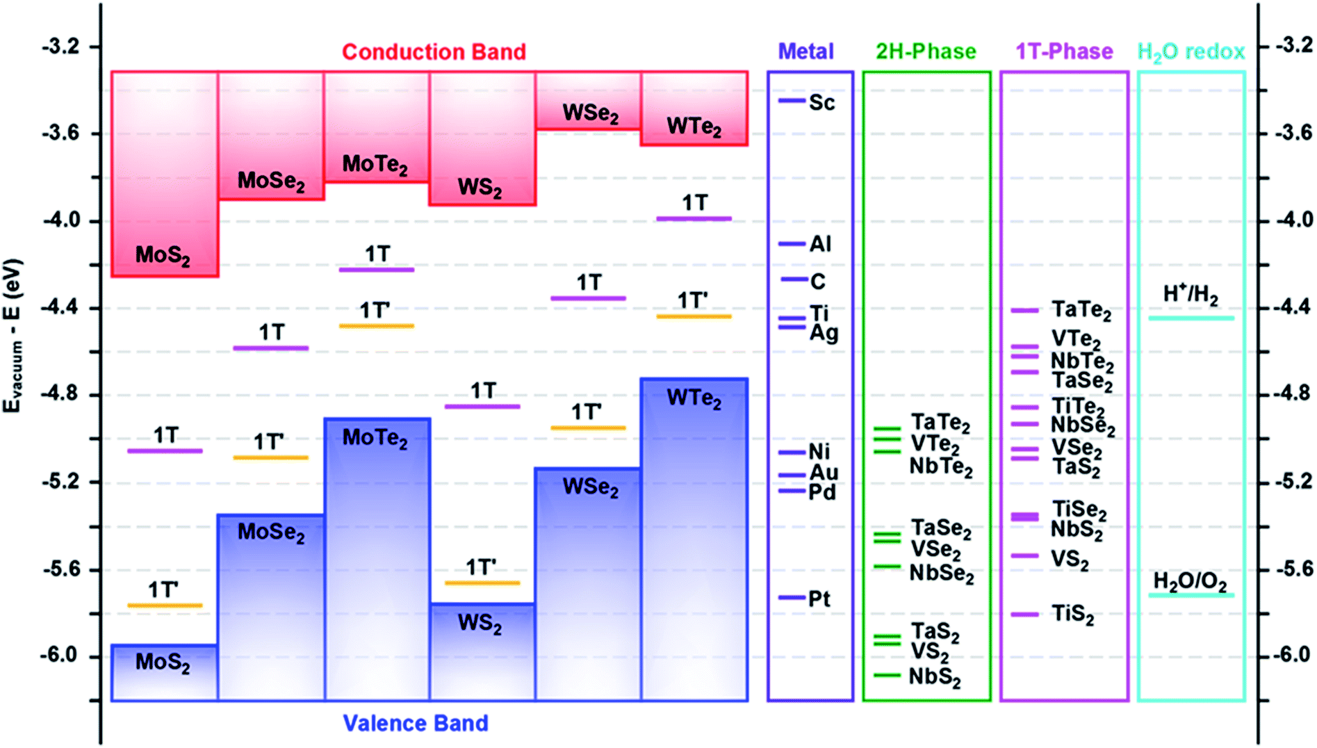
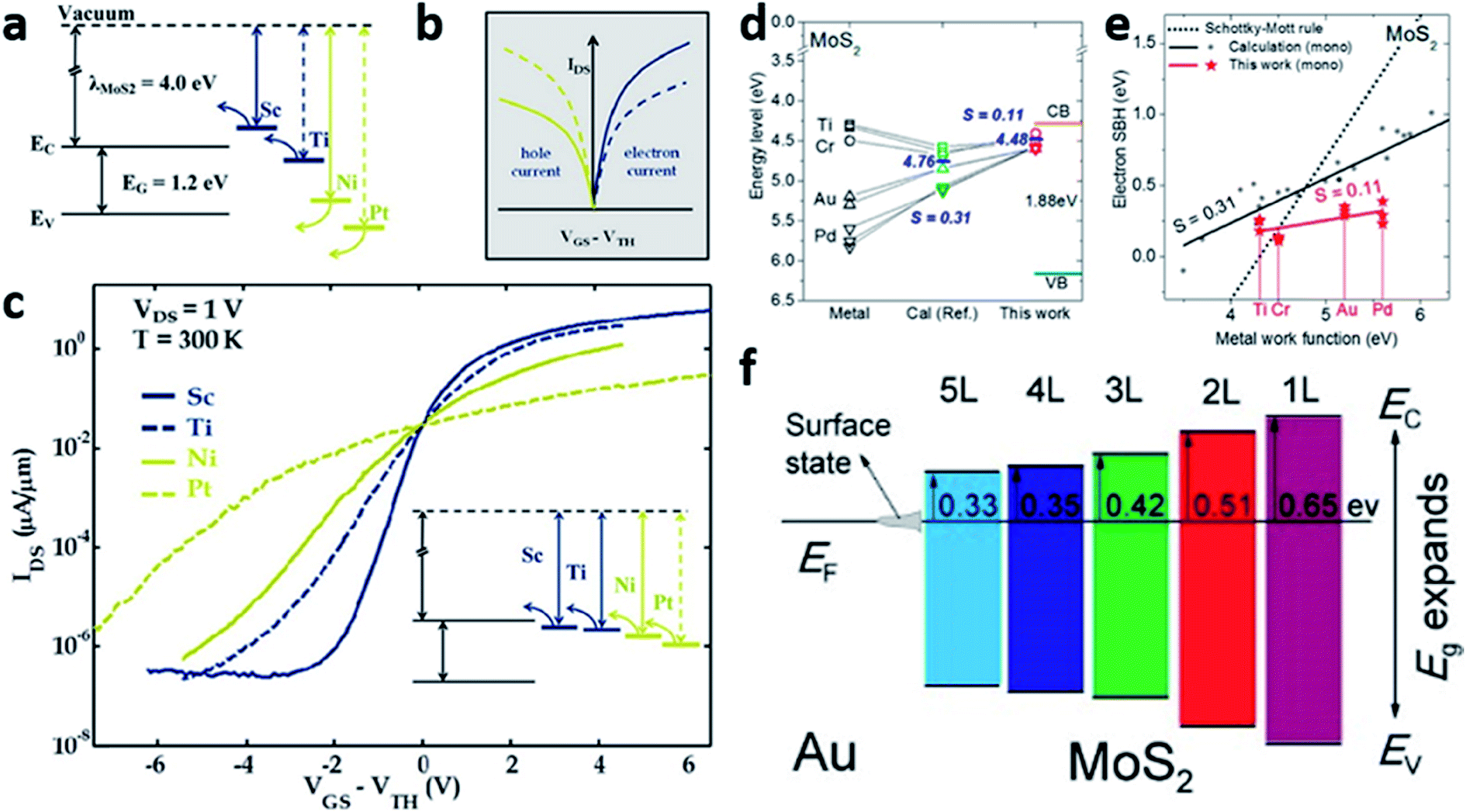
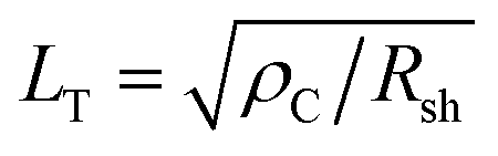 is the effective contact transfer length for the carrier injection, a parameter that describes the distance over which 1/e of the current is transferred to the metal contact (Fig. 3).45–47 For short LT, the current crosses around the contact edge, while for long LT, the current involves larger contact areas.45 This current injection phenomenon, termed as current crowding, imposes device scaling limits because if L < LT, RC increases abruptly.48,49 Therefore, keeping L ≫ 1.5 LT is crucial to avoid high RC and to keep L-independent RC when downscaling devices; consequently, coth(L/LT) ∼ 1, and thus RC = RshLT/W and RT = Rsh(2LT + Lch)/W, where Lch is the channel length. The linear fit of RTvs. Lch plot allows the extraction of 2RC, 2LT and Rsh from the intersection with the RT axis, Lch axis and the slope, respectively. (iv) Four-probe measurements lead to RC = (V2p/Isd − (V4p/Isd) × (L2p/L4p)) × W, where W is the channel width and Isd, V2p (V4p), and L2p (L4p) are the source-drain (probing contacts) current, voltage drops and length, respectively.50 (v) Four-probe FET measurement avoids the potential drop in the sensing probes, and thus RC can be extracted independently for each lead.42 (vi) The Y-function method is more realistic since it allows the extraction of RC from the FET linear region while considering phonon and surface scattering events as well as the voltage drop induced by the SB.51
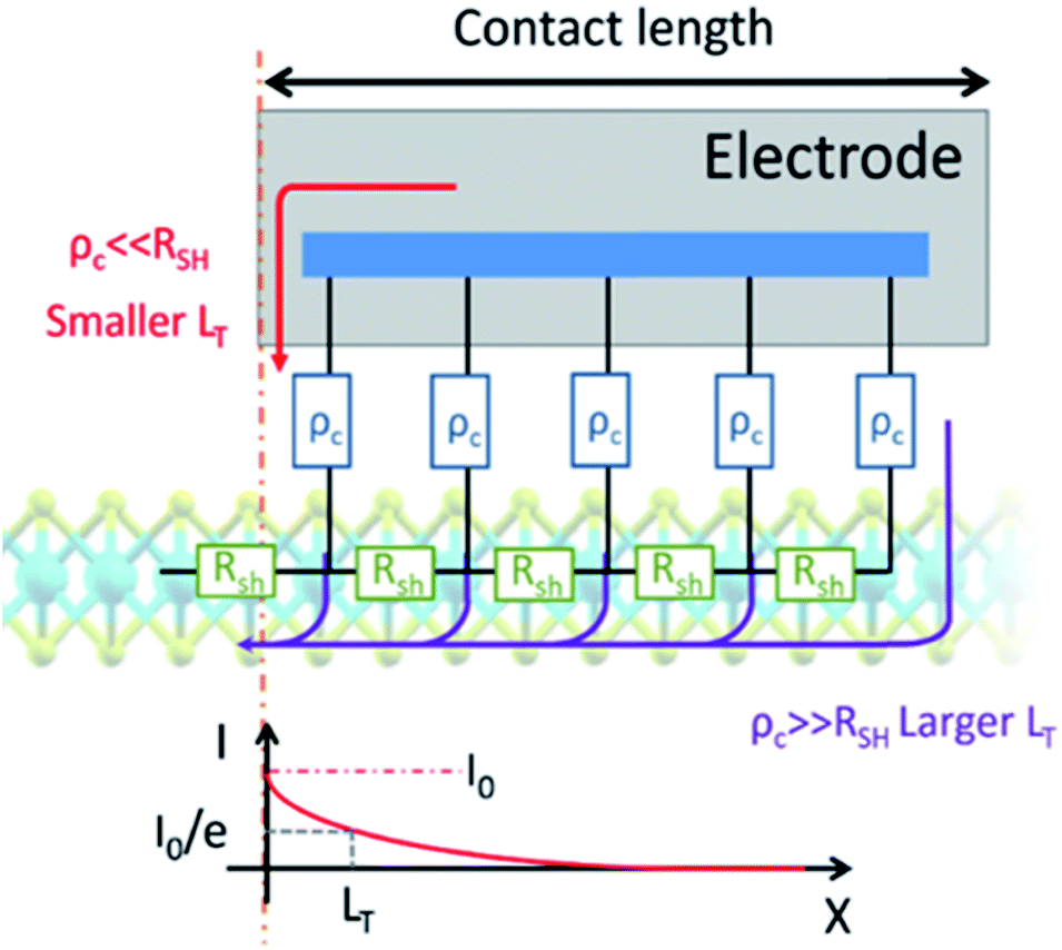
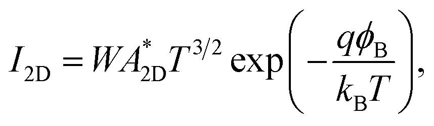
 is the 2D equivalent Richardson constant with m* being the electron effective mass (Table 1).24,49,52–54 It is also noteworthy that TMDs exhibit layer dependent effective mass, for instance the effective mass of MoS2 varies from 0.41m0 to 0.57m0 from monolayer to few-layer.55 At sufficient forward bias, the image charge-induced barrier lowering accounted for by the ideality factor can be extrapolated from q/2.3ηkBT = slope of the linear fitting of the semilog I vs. V or log[I/(1 − exp(−qV/kBT))] vs. V plots.54 Meanwhile, at sufficient reverse bias (qV ≫ kBT)
 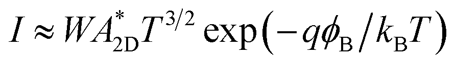 ; therefore, SBH can be calculated from current–temperature measurements as ϕB = (kB/q)(Δln(I/T3/2)/ΔT−1) (Fig. 4a–c).24,35 However, the veracity of the as-extracted SBH should be revised when ϕB < 3kBT or ϕB < 0 because such a SBH is not effective for carrier blocking.31,56,57 Beyond thermionic emission, the applied bias configuration, doping level and temperature can enable direct tunneling (DT; field emission) through a wide-trapezoidal barrier at the quasi-Fermi level and/or thermally assisted Fowler–Nordheim tunneling (FNT; thermionic field emission) through a thin-triangular barrier above the Fermi level but below the top of the SB.58 To discern whether DT or FNT dominates, the ln(I/V2) vs. (I/V) plots should be explored as follows
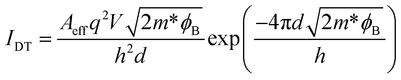
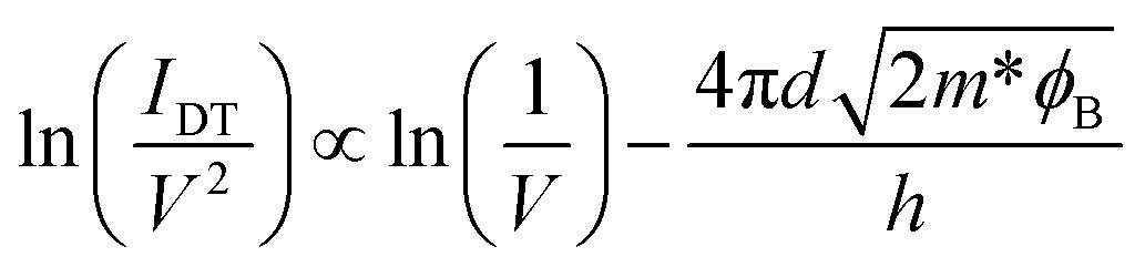
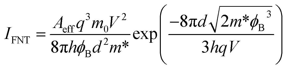
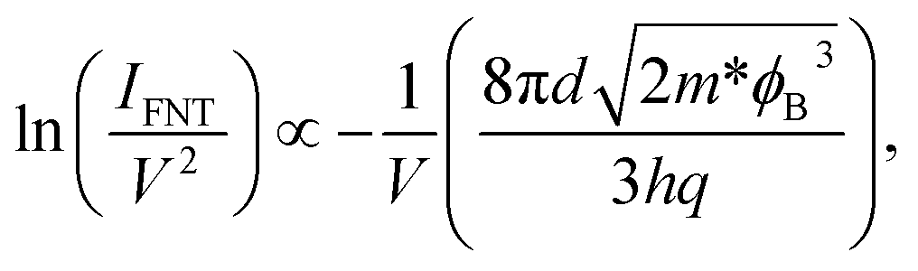
 at different gate bias, and thus VFB can be realized by finding at which Vgs the
  vs. Vgs deviates from linearity (Fig. 4d–f). Alternatively, the thermally assisted tunneling transport can be described as I = Isexp(qV/Φ00), where Is is the saturation current at zero forward voltage and Φ00 is the characteristic energy, both being related as Is ∝ exp(ϕB/Φ00). Accordingly, Is and Φ00 can be extracted from the linear fit of ln(I) vs. V at different temperatures, and ϕB can be extracted by the semi-logarithmic slope of Isvs. 1/Φ00 (Fig. 4g–i).35,64
 , dielectric constant (ε [ε0]), natural scaling length (λ [nm]) for 2 nm thick HfO2 (εox = 25), subthreshold slope (SS [mV dec−1]), and drain-induced barrier lowering (DIBL [mV V−1]) of monolayer TMDs.94,95 Reproduced with permission from ref. 94 © 2013, IEEE; ref. 95 © 2014, Applied Physics Letters