DOI:
10.1039/C8SC02482K
(Edge Article)
Chem. Sci., 2018,
9, 6981-6987
A simple, label-free, electrochemical DNA parity generator/checker for error detection during data transmission based on “aptamer-nanoclaw”-modulated protein steric hindrance†
Received
6th June 2018
, Accepted 15th July 2018
First published on 19th July 2018
Abstract
Versatile DNA logic devices have exhibited magical power in molecular-level computing and data processing. During any type of data transmission, the appearance of erroneous bits (which have severe impacts on normal computing) is unavoidable. Luckily, the erroneous bits can be detected via placing a parity generator (pG) at the sending module and a parity checker (pC) at the receiving module. However, all current DNA pG/pC systems use optical signals as outputs. In comparison, sensitive, facilely operated, electric-powered electrochemical outputs possess inherent advantages in terms of potential practicability and future integration with semiconductor transistors. Herein, taking an even pG/pC as a model device, we construct the first electrochemical DNA pG/pC system so far. Innovatively, a thrombin aptamer is integrated into the input-strand and it functions as a “nanoclaw” to selectively capture thrombin; the electrochemical impedance changes induced by the “nanoclaw/thrombin” complex are used as label-free outputs. Notably, this system is simple and can be operated within 2 h, which is comparable with previous fluorescent ones, but avoids the high-cost labeled-fluorophore and tedious nanoquencher. Moreover, taking non-interfering poly-T strands as additional inputs, a cascade logic circuit (OR-2 to 1 encoder) and a parity checker that could distinguish even/odd numbers from natural numbers (0 to 9) is also achieved based on the same system. This work not only opens up inspiring horizons for the design of novel electrochemical functional devices and complicated logic circuits, but also lays a solid foundation for potential logic-programmed target detection.
Introduction
Since de Silva pioneered the first molecular AND logic gate,1 the development of molecular logic systems based on different materials2–5 has flourished over the past few decades, in which DNA was considered as one of the most promising building blocks. With scientists' constant efforts, fluorescent, colorimetric, electrochemical and other kinds of DNA logic devices/nanoswitches6–15 were fabricated to perform basic, advanced and sophisticated logic functions.16–20 However, most of them used optical signals as outputs which were usually recorded using large/cumbersome instruments, greatly restricting their potential bridge with silicon-based semiconductor logic circuits. In comparison, sensitive, facilely operated, electric-powered electrochemical DNA logic devices possess inherent advantages in terms of potential practicability and future integration with semiconductor transistors, while current electrochemical logic devices are confined to basic logic gates, keypad locks, encoders/decoders, and multi-input/-output circuits,21–23 which could not meet pluralistic logical requirements. Thus, exploring multifunctional electrochemical logic systems that could not only perform novel/specific logic functions, but also engineer various logic circuits is one of the brightest subjects.
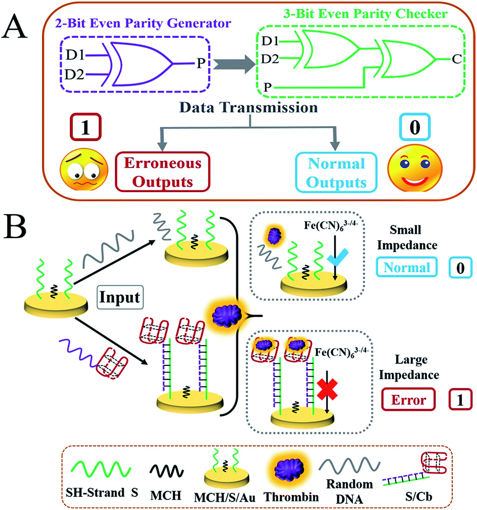
During any kind of data transmission, the occurrence of erroneous bits (which have severe impacts on normal logic computing) is an unavoidable problem.24–27 Luckily, these bits can be detected via placing a parity generator (pG) at the sending module and a parity checker (pC) at the receiving module. As described in the pG/pC operating principles,24–29 an even pG could generate an additional parity bit (P) and add it to the initial binary bits Dn, changing the number of 1's (Σ) in the DnP string to even. For example, if two bits of data (D1 and D2) are to be sent, the 2-bit even pG will endow a binary value to P (the output of pG) in light of the truth table of an XOR gate (see Scheme 1A and Fig. 1A). Afterwards, the D1D2P string generated by the 2-bit even pG will be sent to and checked by the 3-bit even pC (Scheme 1A). If the transmission is normal, the three bits (D1, D2 and P) will not change. The Σ value of the D1D2P string received by the pC remains even, and the pC exhibits a “normal” signal (Scheme 1A, the smiling face) via yielding output C = 0. However, if errors appear during the transmission of the three bits, the Σ value of the received wrong 3-bit string will change to odd (see Table 1), then the pC will give an “alarm” signal (Scheme 1A, the sad face) via producing output C = 1.24–29 All of the above describes the “error detection” procedure of the even pG/pC, and the odd pG/pC qualifies similar functions. Although scientists have made great efforts to advance the pG/pCs, most of the current pG/pCs are constructed upon semiconductor substrates,24–29 and only a few molecular pG/pCs have been achieved based on organic molecules or DNAs using optical (fluorescent or colorimetric) signals as outputs.28,29 To the best of our knowledge, no electrochemical DNA pG/pC system has ever been reported and further endeavours are required to realize it.
 |
| | Scheme 1 (A) Equivalent logic circuit of the 2-bit even pG and 3-bit even pC; the sad and smiling faces represent erroneous and normal outputs, respectively. (B) Schematic illustration of the operating principle of the electrochemical pG/pC system; the red basket indicates the thrombin aptamer that functions as a “nanoclaw”. The blue “√” and red “×” symbols represent favourable and blocked electron transfer, respectively. | |
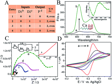 |
| | Fig. 1 (A) Truth table of the 2-bit parity generator (anumber of 1's in the D1D2P string, bstrand Ca, cstrand Cb, dΔRct values); (B) fluorescence spectra of NMM in the absence (a) and presence (b) of Ca strand/K+, the inset shows the CD spectrum of the Ca/thrombin mixture; (C) electrochemical impedance spectra (Nyquist curves) of (a) a bare Au electrode (inset), (b) S/Au, (c) MCH/S/Au, (d) TB/random/MCH/S/Au and (e) TB/Cb/MCH/S/Au; and (D) cyclic voltammetry curves of the different electrodes in (C). The CV (−0.2 to 0.6 V) and EIS (0.1 Hz to 100 kHz) curves were collected in 5 mM [Fe(CN)63−/4−] and 0.1 M KCl aqueous solution. The scan rate for CV was 0.1 V s−1 and the amplitude for EIS was 5 mV. | |
Table 1 Truth table of the 3-bit even pC (anumber of 1's in the D1D2P string, for P = 1: bstrand TCb, cstrand Cb, dstrand Ca, eΔRct values of Au electrodes)
| Entry |
Inputs |
Output |
∑
a
|
States |
| D1b |
D2c |
Pd |
Ce |
| 1 |
0 |
0 |
0 |
0 |
0, even |
Ok |
| 2 |
0 |
1 |
0 |
1 |
1, odd |
Error |
| 3 |
1 |
0 |
0 |
1 |
1, odd |
| 4 |
1 |
1 |
0 |
0 |
2, even |
Ok |
| 5 |
0 |
0 |
1 |
1 |
1, odd |
Error |
| 6 |
0 |
1 |
1 |
0 |
2, even |
Ok |
| 7 |
1 |
0 |
1 |
0 |
2, even |
| 8 |
1 |
1 |
1 |
1 |
3, odd |
Error |
Electrochemical impedance spectroscopy (EIS) is widely applied to characterize the modification procedures of electrodes.30 The semicircle region appearing at high frequencies reflects the limited charge-transfer process, and the interfacial charge-transfer resistance (Rct) can be estimated according to the diameter of the semicircle. Actually, the EIS signals possess the inherent merits of facile testing, low cost, high sensitivity, and reliable reproducibility and have been used to probe various electrochemical biosensors.31–33 In contrast, as far as we know, DNA logic systems that are signalled by EIS signals have rarely been reported.34 According to previous reports, single-strand DNA and other secondary structures present different repelling abilities towards the EIS probe [Fe(CN)63−/4−]. And the flexibility/specificity of an aptamer to bind with macromolecules (such as protein) also enables “target-induced steric hindrance”35 to be an efficient output signal to operate electrochemical DNA logic devices.
Herein, taking an even pG/pC as model device, we construct the first electrochemical DNA pG/pC system so far for error detection during data transmission. Innovatively, a thrombin aptamer (TBA15) is integrated into the input-strand and it functions as the “nanoclaw” to selectively capture thrombin (TB); the electrochemical impedance changes induced by the “nanoclaw/TB” complex are used as label-free outputs. Notably, this system is simple and can be operated within 2 h, which is comparable with previous fluorescent ones, but avoids the expensive labeled-fluorophore and tedious nanoquencher. Moreover, taking non-interfering poly-T strands as additional inputs, a cascade logic circuit (OR-2 to 1 encoder) and a parity checker that could distinguish even/odd numbers from natural numbers (0 to 9) are also achieved based on the same system.
Results and discussion
Operating principle of the electrochemical pG/pC system
As demonstrated above, the XOR gate is the basis of the pG/pC system28,29 and the presence of the TB aptamer (TBA15, the “nanoclaw”)36,37 to capture thrombin efficiently is the key to obtaining a sufficiently high signal-to-noise (S/N) ratio. Thus, verification experiments were explored initially before the operation of the pG/pC. As shown in Scheme 1B, a Au electrode treated with SH-DNA (green strand) and blocked by MCH (MCH/S/Au) was taken as the universal platform for the pG/pC. The dramatically enhanced fluorescence of NMM28 and unique CD peaks (negative peak at around 260 nm and a positive one at around 290 nm, Fig. 1B) implied the effective binding between the nanoclaw and TB,36 providing an ideal secondary structure for adequate EIS changes. Before modification, the bare Au electrode exhibited a small Rct and peak-to-peak difference and large peak current (Fig. 1C(a) and D(a)). After modification with SH-DNA and blocking by MCH, the Rct and peak-to-peak difference of the MCH/S/Au electrode increased gradually accompanied by a decrease of peak current due to the electrostatic repulsion of negatively charged SH-DNA towards the [Fe(CN)63−/4−] probe, Fig. 1C(c) and D(c), indicating the successful fabrication of the platform.
Furthermore, the importance of the input strands and “nanoclaw” was evaluated. In the presence of random strand R (grey strand) without the nanoclaw (Scheme 1B), it could neither hybridize the SH-strand nor capture TB; the Rct presented only slight changes as for the weak nonspecific binding (Fig. 1C(d)). In contrast, in the presence of strand Cb (purple strand) that was integrated with the nanoclaw (the red basket), it could hybridize with the SH-strand and the nanoclaw will capture TB to form the “nanoclaw/TB” complex, leading to a significantly enhanced Rct (Fig. 1C(e)). The peak-to-peak difference and peak current (Fig. 1D) were in good accordance with the corresponding EIS changes. The sufficiently high S/N ratio appearing in the EIS and CV curves proved not only the progressive modification of the Au electrode, but also the feasibility of Rct to be the output of the electrochemical DNA pG/pC system. More accurately, the Rct changes (ΔRct) were used as the outputs and the threshold value was set as 12 kΩ to distinguish the positive and negative outputs. ΔRct = Rct (a) − Rct (i), where Rct (i) and Rct (a) represent the Rct of the initial platform and that after adding inputs/TB, respectively.
The 2-bit parity generator
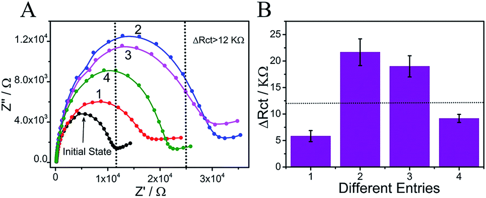
As illustrated in our previous work,28,29 the pG/pC system for “error detection” during data transmission consists of an n-bit pG and an (n + 1)-bit pC. Herein, a 2-bit even pG/3-bit even pC was targeted as the model and the 2-bit even pG was constructed at first according to the principle of the XOR gate (truth table, Fig. 1A). The detailed hybridization of different strands is presented in Fig. S1–S3.† The ΔRct value was defined as output P. As depicted in Scheme 2, strands Ca (blue strand) and Cb (purple strand) that was integrated with the “nanoclaw” and could partially hybridize with different parts of the SH-strand acted as inputs D1 and D2, respectively. In the absence of any input (entry 1 of Scheme 2), TB could not be captured and immobilized on the surface of the electrode tightly. The final electrode exhibits weak repelling ability towards [Fe(CN)63−/4−], producing output P = 0. In the presence of any input, Ca or Cb will partially hybridize with S and form duplex S/Ca or S/Cb (entries 2 and 3 of Scheme 2); the “nanoclaw” at the end of input strands could capture TB effectively and enhance the steric hindrance evidently, yielding output P = 1 (Fig. S4†). However, in the presence of both input strands, the pre-reaction of Ca and Cb will form more stable duplex Ca/Cb than S/Ca or S/Cb.29 The generated duplexes can hardly hybridize with S anymore and most of them will be scoured off during the washing step. And only an slightly increased Rct (P = 0) was obtained after adding TB. Fig. 2A illustrates the detailed EIS curves under different input combinations. The input and output states can be further identified by the ΔRct column bars (Fig. 2B), which matched the truth table (Fig. 1A) well, indicating the appropriate operation of the 2-bit even pG. The PAGE verification of strand reactions is shown in Fig. S5.† The corresponding optimization of the concentrations of TB and input strands is shown in Fig. S6 and S7,† and the DNA sequences used in this work are given in Table S1.†
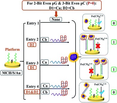 |
| | Scheme 2 Detailed DNA hybridization of different entries for the 2-bit even pG and 3-bit even pC (P = 0 states). Strands Ca and Cb act as inputs D1 and D2, respectively. | |
 |
| | Fig. 2 (A) Electrochemical impedance spectra of the MCH/S/Au electrode under different entries: (1) TB/MCH/S/Au, (2) TB/Cb/MCH/S/Au, (3) TB/Ca/MCH/S/Au, and (4) TB/(Ca + Cb)/MCH/S/Au. (B) The ΔRct column bars of the different entries. | |
The 3-bit parity checker
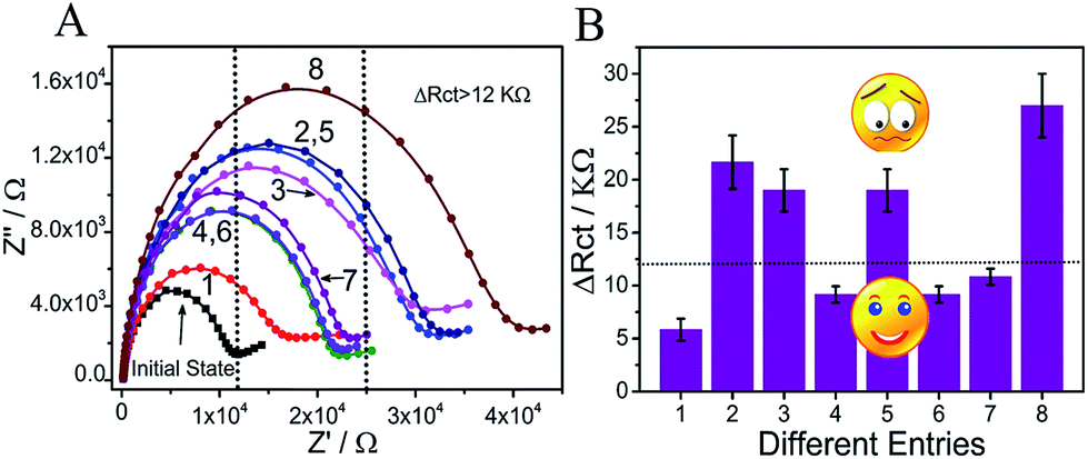
After constructing the 2-bit even pG, a 3-bit even pC was further constructed to achieve the “error detection” function. The platform of the pC was still the MCH/S/Au electrode, to which the third input P was brought to meet the requirements. The input variations of the 3-bit even pC that are demonstrated in Table 1 can be separated into two parts.24,28,29 For the first part (P = 0 states, entries 1 to 4), the outputs of the pC (ΔRct was defined as output C now) were just the same as those of the above-constructed 2-bit even pG. The logic circuit can be considered as an XOR gate, in which the DNA reactions were analogous to the 2-bit pG and have been illustrated above. For the second part (P = 1 states, entries 5 to 8), input P actually executes the XNOR function that is complementary to both inputs (D1 and D2) to change the number of 1's (Σa) in the DnP string to even.24,28,29 The detailed DNA hybridizations of various entries (entries 5 to 8) are shown in Scheme 3. Herein, the third strand TCb, that was 5 thymine units (orange part) longer than Cb at the 3′ end, was introduced as another input to achieve the function of the 3-bit pC (P = 1 states). Similar to previous reports,24,28,29 the inputs Ca, Cb and TCb were redefined as follows to execute the 3-bit even pC (P = 1 states) properly, Ca acted as input P, while strand TCb and Cb functioned as inputs D1 and D2, respectively.
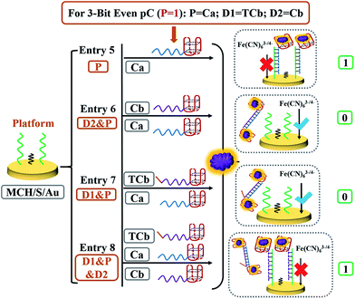 |
| | Scheme 3 Detailed DNA hybridization of different entries for the 3-bit even pC (P = 1 states). Strands Ca, TCb and Cb function as inputs P, D1 and D2, respectively. | |
In the presence of input P (entry 5), the DNA interaction was similar to that of entry 3 (Scheme 2), yielding output C = 1. In the coexistence of inputs D2 and P (entry 6), the operation was the same as that of entry 4, yielding output C = 0. For entry 7 (inputs D1 and P), the pre-reaction of Ca and TCb will generate more stable duplex Ca/TCb, resulting in a slightly changed Rct after reacting with TB (output C = 0). However, in the presence of all three inputs, TCb (or Cb) will hybridize with Ca and generate duplex Ca/TCb (or Ca/Cb). The resident Cb (or TCb) could still hybridize with S and the nanoclaw will capture TB and finally increase the Rct on the surface of the electrode, yielding output C = 1 (as an example, the interaction between TCb and Ca is shown in Scheme 3). Fig. 3A presents the ΔRct column bars under different input variations. The erroneous (sad face) and normal transmission (smiling face) can be easily distinguished.
 |
| | Fig. 3 (A) Electrochemical impedance spectra of the MCH/S/Au electrode under 8 different entries: entry (1) to (4) were just the same as those in Fig. 2A; (5) input P (Ca) and TB; (6) input D2 (Cb), P (Ca) and TB; (7) input D1 (TCb), P (Ca) and TB; (8) input D1 (TCb), P (Ca) and D2 (Cb) and TB; (B) the ΔRct column bars of different entries. The sad and smiling faces represent erroneous and normal transmission, respectively. | |
Cascade logic circuit and parity checker for natural numbers
There is no doubt that a versatile system that could perform pluralistic logical functions will exhibit giant advantages. Herein, based on the universal platform (MCH/S/Au electrode), we further constructed a cascade logic circuit [OR-2 to 1 encoder] and a parity checker for discriminating even/odd natural numbers (0–9). For the cascade logic circuit, strands Cb and TCb functioned as the input of the OR gate, whose output was the final state of the Au electrode (Cb/MCH/S/Au and TCb/MCH/S/Au were output “1”, and MCH/S/Au was output “0”). Subsequently, the output of the OR gate was applied as one input of the downstream 2 to 1 encoder, of which another input is the poly-T strand (T30) that will hardly influence the Rct. And the output definitions were just the same with the pG/pC. Fig. 4B shows the ΔRct column bars under various input combinations; the input–output mapping states fitted well with the corresponding truth table (Fig. 4C), suggesting the proper operation of the OR-2 to 1 encoder. Compared with simple logic gates, cascade logic circuits could perform more complicated logic computation.
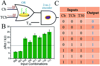 |
| | Fig. 4 (A) Equivalent logic symbol of the cascade logic circuit [OR-2 to 1 encoder]; (B) the ΔRct column bars under various input variations; and (C) the corresponding truth table. | |
Different from the pG/pC devices that were used to detect erroneous bits through data transmission, the parity checker for natural numbers could distinguish the even/odd numbers from 0 to 9.38–40 Here, different poly-T strands (T20, T30 and T40) and strand Ca were used as the inputs of the parity checker for natural numbers. The decimal numbers were transformed to binary-coded decimal numbers initially, and strands T20, T30, T40 and Ca functioned as the four codes, respectively. As presented in Fig. 5B, the even/odd numbers (0 to 9) can be facilely identified according to the ΔRct column bars under different input variations. All the above indicated the universal applicability of the system.
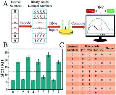 |
| | Fig. 5 (A) Schematic illustration of the parity checker for natural numbers (0–9) based on the universal system; (B) the ΔRct column bars under different input combinations; and (C) the truth table. | |
Conclusion
To summarize, by utilizing the “aptamer-nanoclaw”-modulated protein steric hindrance as label-free output and taking an even pG/pC as model device, we constructed the first electrochemical DNA pG/pC system so far. This system presented obvious advantages: firstly, this pG/pC system was electrochemical, which largely promotes its future integration with semiconductor transistors; secondly and innovatively, a thrombin aptamer was integrated into the input-strand and acted as a “nanoclaw” to selectively capture thrombin, enabling the operation of other electrochemical DNA logic devices; thirdly, this system was simple, low cost and can be operated within 2 h, which was comparable with previous fluorescent ones; last but not least, a cascade logic circuit and a parity checker for distinguishing even/odd natural numbers (0 to 9) were also fabricated based on the same system, which greatly met the requirements of pluralistic logical functions. This work not only opens up inspiring horizons for the design of novel electrochemical functional devices and complicated logic circuits, but also lays a solid foundation for potential logic-programmed target detection.
Experimental section
Chemicals
All the DNAs were provided by Shanghai Sangon Biotechnology (Shanghai, China); a thrombin aptamer (TBA 15) was used as a “nanoclaw” and integrated into the input strands Ca and Cb. Thrombin (TB) and 6-mercaptohexanol (MCH) were purchased from Sigma Aldrich (USA). Tris (2-carboxyethyl) phosphine hydrochloride (TCEP) was purchased from Bio Basic Inc (Markham Ontario, Canada). K3Fe[CN]6 and K4Fe[CN]6 were obtained from Xilong Chemical Co. Ltd. (Guangdong, China). NMM (N-methyl mesoporphyrin IX, a kind of porphyrin dye that could generate an enhanced fluorescence signal after binding with G-quadruplex) was provided by J&K (Beijing, China). Tris–HCl S-buffer (20 mM Tris, 100 mM NaCl, 5 mM TCEP, pH 7.4) was used to dissolve SH-DNA. Tris–HCl M-buffer (20 mM Tris, 2 mM MCH, pH 7.4) was applied to block the electrode and decrease nonspecific adsorption. Tris–HCl W-buffer (5 mM Tris, pH 7.4) acted as the washing buffer. Other DNAs were dissolved with 1× HEPES buffer (25 mM HEPES, 10 mM KCl, 100 mM NaCl, pH 7.4). Distilled water was purified using a Millipore system.
Apparatus
EIS curves were collected on a Zahner Zennium electrochemical workstation (ZAHNER-Elektrik, Germany) and CV curves were measured on a CHI 760E electrochemical workstation (Shanghai Chenhua Equipments, China). A conventional three electrode electrochemical system was used, in which Ag–AgCl acted as the reference electrode, a gold electrode (about 2 mm in diameter) acted as the working electrode and Pt wire functioned as the counter electrode. The CV curves (−0.2 to 0.6 V) and EIS spectra (0.1 Hz to 100 kHz) were collected in 5 mM [Fe(CN)63−/4−] and 0.1 M KCl aqueous solution. The scan rate for CV was 0.1 V s−1 and the oscillation potential for EIS was 5 mV.
Preparation of the initial platform (MCH/S/Au electrode)
A Au electrode was first polished with 1 μm and 0.3 μm alumina slurries (α-Al2O3) and ultrasonicated in distilled water several times. Then, the electrode was treated by electrochemical cleaning in 0.1 mM H2SO4, and a CV test was performed for about 150 cycles in the potential range of −0.3 to 1.5 V with a scan rate of 0.1 V s−1 to obtain the characteristic peaks of the Au electrode. After that, the electrode was washed with distilled water and dried under nitrogen gas.
Before modification, SH-DNA was dissolved in Tris–HCl S-buffer and incubated for 1 h in the dark to reduce the disulfide bonds. Then, 10 μL 1 μM SH-DNA was dropped on the bare Au electrode and capped with a centrifuge overnight at room temperature. Then the S/Au electrode was immersed in Tris–HCl M-buffer to reduce nonspecific adsorption. After washing with Tris–HCl W-buffer, the MCH/S/Au electrode was obtained.
Operation of the pG/pC and other logic devices
For the typical operation of the pG/pC, the MCH/S/Au electrode was immersed in solutions of different concentrations of Ca and Cb (for entries 2, 3, and 5) or a pre-mixture of Ca/Cb and Ca/TCb (for entries 4, 6, 7, and 8) and reacted at room temperature for about 0.5 h. After washing with Tris–HCl W-buffer and drying under mild nitrogen gas, 100 nM TB was dropped on the surface of the different Au electrodes and allowed to react for about 1 h. Finally, the EIS curves of the Au electrodes were measured. The operation of the cascade logic circuit and parity checker for natural numbers was just analogous to the pG/pC, but different DNA strands were used. The concentrations of the different strands were 1 μM Ca, 0.8 μM Cb, 0.8 μM TCb, and 200 nM for all the poly-T strands.
CD and fluorescence spectra
CD spectra were measured from 220 to 320 nm in 1 mm path-length cuvettes and averaged from three scans on a JASCO J-820 spectropolarimeter (Tokyo, Japan). Before the fluorescence test, 500 nM Ca and 1 μM NMM were mixed in 1× HEPES buffer and incubated at room temperature for about 1 h. Then the spectra of Ca/NMM were collected on a Cary Eclipse Fluorescence Spectrophotometer (Agilent Technologies, USA). The spectra were collected from 550 to 750 nm (excitation wavelength: 399 nm; excitation and emission slit widths: 10 and 20 nm, respectively).
Conflicts of interest
There are no conflicts to declare.
Acknowledgements
This work was supported by the National Natural Science Foundation of China (No. 21427811 & 21675151).
Notes and references
- P. A. de Silva, N. H. Q. Gunaratne and C. P. McCoy, Nature, 1993, 364, 42–44 CrossRef.
- J. Andreasson and U. Pischel, Chem. Soc. Rev., 2015, 44, 1053–1069 RSC.
- E. Shapiro and B. Gil, Nat. Nanotechnol., 2007, 2, 84 CrossRef PubMed.
- M. N. Stojanovic, D. Stefanovic and S. Rudchenko, Acc. Chem. Res., 2014, 47, 1845–1852 CrossRef PubMed.
- J. Elbaz, O. Lioubashevski, F. Wang, F. Remacle, R. D. Levine and I. Willner, Nat. Nanotechnol., 2010, 5, 417–422 CrossRef PubMed.
- I. Willner, B. Shlyahovsky, M. Zayats and B. Willner, Chem. Soc. Rev., 2008, 37, 1153–1165 RSC.
- S. Mailloux, Y. V. Gerasimova, N. Guz, D. M. Kolpashchikov and E. Katz, Angew. Chem., Int. Ed., 2015, 54, 6562–6566 CrossRef PubMed.
- A. Prokup and A. Deiters, Angew. Chem., Int. Ed., 2014, 53, 13192–13195 CrossRef PubMed.
- L. Feng, Z. Lyu, A. Offenhausser and D. Mayer, Angew. Chem., Int. Ed., 2015, 54, 7693–7697 CrossRef PubMed.
- L. Adleman, Science, 1994, 266, 1021–1024 CrossRef PubMed.
- L. Qian and E. Winfree, Science, 2011, 332, 1196 CrossRef PubMed.
- G. Seelig, D. Soloveichik, D. Y. Zhang and E. Winfree, Science, 2006, 314, 1585 CrossRef PubMed.
- W. Engelen, L. H. Meijer, B. Somers, T. F. de Greef and M. Merkx, Nat. Commun., 2017, 8, 14473 CrossRef PubMed.
- J. Li, A. A. Green, H. Yan and C. Fan, Nat. Chem., 2017, 9, 1056–1067 CrossRef PubMed.
- X. Qu, S. Wang, Z. Ge, J. Wang, G. Yao, J. Li, X. Zuo, J. Shi, S. Song, L. Wang, L. Li, H. Pei and C. Fan, J. Am. Chem. Soc., 2017, 139, 10176–10179 CrossRef PubMed.
- D. Fan, E. Wang and S. Dong, Mater. Horiz., 2017, 4, 924–931 RSC.
- D. Fan, K. Wang, J. Zhu, Y. Xia, Y. Han, Y. Liu and E. Wang, Chem. Sci., 2015, 6, 1973–1978 RSC.
- D. Fan, J. Zhu, Y. Liu, E. Wang and S. Dong, Nanoscale, 2016, 8, 3834–3840 RSC.
- D. Fan, E. Wang and S. Dong, Nano Res., 2017, 10(8), 2560–2569 CrossRef.
- D. Fan, C. Shang, W. Gu, E. Wang and S. Dong, ACS Appl. Mater. Interfaces, 2017, 9, 25870–25877 CrossRef PubMed.
- H. Li, W. Hong, S. Dong, Y. Liu and E. Wang, ACS Nano, 2014, 8, 2796–2803 CrossRef PubMed.
- W. Hong, Y. Du, T. Wang, J. Liu, Y. Liu, J. Wang and E. Wang, Chem.–Eur. J., 2012, 18, 14939–14942 CrossRef PubMed.
- X. Yu, M. Li, T. Li, S. Zhou and H. Liu, Nanoscale, 2016, 8, 20027–20036 RSC.
- M. Balter, S. Li, J. R. Nilsson, J. Andreasson and U. Pischel, J. Am. Chem. Soc., 2013, 135, 10230–10233 CrossRef PubMed.
- S. Mandal, D. Mandal and S. K. Garai, Opt. Fiber Technol., 2014, 20, 120–129 CrossRef.
- A. Kumar and S. K. Raghuwanshi, Opt. Fiber Technol., 2014, 47, 2117–2140 Search PubMed.
- S. Kumar, Chanderkanta and A. Amphawan, Opt. Commun., 2016, 364, 195–224 CrossRef.
- D. Fan, E. Wang and S. Dong, Chem. Sci., 2017, 8, 1888–1895 RSC.
- D. Fan, E. Wang and S. Dong, ACS Appl. Mater. Interfaces, 2017, 9, 1322–1330 CrossRef PubMed.
- E. Xiong, X. Zhang, Y. Liu, J. Zhou, P. Yu, X. Li and J. Chen, Anal. Chem., 2015, 87, 7291–7296 CrossRef PubMed.
- L. Wang, R. Ma, L. Jiang, L. Jia, W. Jia and H. Wang, Biosens. Bioelectron., 2017, 92, 390–395 CrossRef PubMed.
- Q. Wang, Z. Zhou, Y. Zhai, L. Zhang, W. Hong, Z. Zhang and S. Dong, Talanta, 2015, 141, 247–252 CrossRef PubMed.
- D. Li, S. Song and C. Fan, Acc. Chem. Res., 2010, 43, 631–641 CrossRef PubMed.
- J. Elbaz, B. Shlyahovsky, D. Li and I. Willner, ChemBioChem, 2008, 9, 232–239 CrossRef PubMed.
- S. S. Mahshid, S. Camire, F. Ricci and A. Vallee-Belisle, J. Am. Chem. Soc., 2015, 137, 15596–15599 CrossRef PubMed.
- D. Zhao, X. Dong, N. Jiang, D. Zhang and C. Liu, Nucleic Acids Res., 2014, 42, 11612–11621 CrossRef PubMed.
- S. Chen, P. Liu, K. Su, X. Li, Z. Qin, W. Xu, J. Chen, C. Li and J. Qiu, Biosens. Bioelectron., 2018, 99, 338–345 CrossRef PubMed.
- K. He, Y. Li, B. Xiang, P. Zhao, Y. Hu, Y. Huang, W. Li, Z. Nie and S. Yao, Chem. Sci., 2015, 6, 3556–3564 RSC.
- R.-R. Gao, S. Shi, Y. Zhu, H.-L. Huang and T.-M. Yao, Chem. Sci., 2016, 7, 1853–1861 RSC.
- M. Li, X. Yu and H. Liu, Electrochim. Acta, 2016, 220, 562–572 CrossRef.
Footnote |
| † Electronic supplementary information (ESI) available: Table S1 and Fig. S1–S7. See DOI: 10.1039/c8sc02482k |
|
| This journal is © The Royal Society of Chemistry 2018 |
Click here to see how this site uses Cookies. View our privacy policy here. 
 Open Access Article
 This Open Access Article is licensed under a Creative Commons Attribution-Non Commercial 3.0 Unported Licence
 ab and
Shaojun
Dong
ab and
Shaojun
Dong