
 Open Access Article
 This Open Access Article is licensed under a Creative Commons Attribution-Non Commercial 3.0 Unported Licence
Characteristics of atomic layer deposited Gd2O3 on n-GaN with an AlN layer
Hogyoung Kim *a,
Hee Ju Yunb and
Byung Joon Choi*b
*a,
Hee Ju Yunb and
Byung Joon Choi*b
aDepartment of Visual Optics, Seoul National University of Science and Technology (Seoultech), Seoul 01811, Republic of Korea. E-mail: hogyoungkim@gmail.com
bDepartmet of Materials Science and Engineering, Seoul National University of Science and Technology (Seoultech), Seoul 01811, Republic of Korea. E-mail: bjchoi@seoultech.ac.kr
First published on 19th December 2018
Abstract
The interfacial and electrical properties of atomic layer deposited Gd2O3 with an AlN layer on n-GaN were investigated. According to X-ray photoelectron spectroscopy spectra, the formation of Ga–O bonds that is significant near the Gd2O3/GaN interface was suppressed near the AlN/Gd2O3/GaN and Gd2O3/AlN/GaN interfaces. Larger amounts of oxygen atoms across the dielectric layers were observed for AlN/Gd2O3/GaN and Gd2O3/AlN/GaN junctions, which in turn produced the dominant peak corresponding to O–Al bonds. The flatband voltage shift in capacitance–voltage hysteresis characteristics was highest for the Gd2O3/AlN/GaN junction, indicating the highest interface and oxide trap densities. In addition, AlN/Gd2O3/GaN and Gd2O3/AlN/GaN junctions showed the highest interface state densities in the energy ranges of 0.1–0.2 eV and 0.4–0.6 eV, respectively. The reverse leakage currents were explained by Fowler–Nordheim (FN) for Gd2O3/GaN and AlN/Gd2O3/GaN junctions and by trap assisted tunneling (TAT) for the Gd2O3/AlN/GaN junction.
1. Introduction
Among rare earth (RE) oxide based materials, gadolinium oxide (Gd2O3) has been considered as a promising material for application in next-generation complementary metal–oxide–semiconductor (CMOS) transistors, because Gd2O3 has a wide band gap (∼6.0 eV) with permittivity values of 10–14 for the epitaxial cubic phase, optimum band offset values with respect to Si, and high thermodynamic stability.1–3 Gd2O3 has also been considered as a gate oxide in Ge-based MOS devices4 and as a passivation layer for GaAs-based electronic devices.5 Upon subjection to a forming gas treatment, the atomic layer deposition (ALD) grown Gd2O3 layer showed promising dielectric behavior, with no hysteresis and reduced interface trap density.6Plasma-enhanced chemical vapor deposition (PECVD)-grown SiNx has been used as an effective passivation material to suppress the current collapse in AlGaN/GaN metal–insulator–semiconductor heterostructure field-effect transistor (MISHFET).7 High-k dielectric oxides such as Al2O3 and HfO2 have also been employed as a passivation layer in AlGaN/GaN high electron mobility transistors (HEMTs).8,9 However, it was shown that high density of deep (and slow) interface states exist near the Al2O3/(Al)GaN interface.10,11 Hence, an alternative passivation method using an AlN layer has been considered for GaN-based devices.12–14 It was demonstrated that the plasma enhanced atomic layer deposition (PEALD)-AlN as interfacial passivation layer is beneficial to improve the quality of Al2O3(HfO2)/InGaAs interface, featuring good electrical characteristics and low interface trap density.15,16 Wu et al. also observed similar passivation effect in Al2O3/GaN structure using a 2 nm thick AlN.17 Due to the easy crystallization of AlN, however, the reverse leakage current become high when employing an AlN layer in the dielectric layer.
In our previous work, we found that the tunneling barrier height in Al2O3/GaN interface with a 1 nm thick AlN interlayer was lower than 1.0 eV, which could be due to the inferior Al2O3 film quality.18 We also observed in Pt/AlN/n-GaN junctions with different AlN thicknesses that the formation of AlN layer near the AlN/GaN interface was observed clearly when the AlN thickness is above 1.5 nm.19 These suggest that at least 2 nm thick AlN grown on GaN will be beneficial to passivate the GaN surface and to improve the overgrown film quality. Although molecular beam epitaxy (MBE) grown Gd2O3 on GaN has been investigated,20,21 there is little knowledge regarding the interface characteristics of ALD-Gd2O3 on GaN. In this work, we comparatively investigated the interfacial and electrical properties of Gd2O3 on GaN with an AlN layer.
2. Experimental
Hydride vapor phase epitaxy (HVPE)-grown, n-type, c-plane (0001) GaN substrate (thickness: 300 μm, carrier concentration: 2 × 1017 cm−3) purchased from Lumistal (Korea) was used in this work. After cutting the wafer into small pieces, some of them were loaded into a thermal ALD chamber (Atomic classic, CN-1, Korea) after cleaning process in a HCl![[thin space (1/6-em)]](https://www.rsc.org/images/entities/char_2009.gif) :H2O (1:1) solution, and three different methods to deposit dielectric layers were applied on the prepared GaN substrates. (i) 1.7 nm thick Gd2O3 layer was directly deposited on the GaN surface at 250 °C with (RCp)2Gd(L) (Air Liquide, USA) as the Gd precursor and H2O as the oxidant (denoted as Gd2O3). (ii) After depositing 1.7 nm thick Gd2O3 on the GaN surface using the same method in (i), the temperature was ramped up to 350 °C to deposit 1.3 nm thick AlN layer using trimethylaluminum (TMA) and NH3 as precursors (denoted as AlN/Gd2O3). (iii) After depositing 2 nm thick AlN on the GaN surface using the same method in (ii), 1.7 nm thick Gd2O3 was deposited using the same method in (i) (denoted as Gd2O3/AlN). The schematic layer structures of three samples are presented in Fig. 1. The thicknesses of the films were measured using a FS-1 multi-wavelength ellipsometer (Film Sense, USA). Depth resolved X-ray photoelectron spectroscopy (XPS) measurements (PHI 5000 VersaProbe, ULVAC PHI, Japan) including sputter etch treatment were carried out using a monochromatic Al Kα X-ray source (beam energy: 1486.6 eV, spot size: 100 × 100 μm2) to observe the chemical reaction near the dielectric/GaN interface. Due to charging effects that result in a shift in binding energy, the binding energy scale was calibrated by using the adventitious C 1s peak to 284.6 eV. The collected XPS data were analyzed using Multipak software. To characterize the electrical properties, metal–insulator–semiconductor (MIS) diodes were fabricated with a Pt Schottky electrode (diameter: 500 μm, thickness: 50 nm) and an Al back contact (thickness: 100 nm). Capacitance–voltage (C–V) and current–voltage (I–V) measurements were performed using a HP 4284A LCR meter and Keithley 238 current source, respectively. During the C–V measurements, an AC voltage of 30 mV with various frequencies was applied to the device so that small signal conditions were realized.
:H2O (1:1) solution, and three different methods to deposit dielectric layers were applied on the prepared GaN substrates. (i) 1.7 nm thick Gd2O3 layer was directly deposited on the GaN surface at 250 °C with (RCp)2Gd(L) (Air Liquide, USA) as the Gd precursor and H2O as the oxidant (denoted as Gd2O3). (ii) After depositing 1.7 nm thick Gd2O3 on the GaN surface using the same method in (i), the temperature was ramped up to 350 °C to deposit 1.3 nm thick AlN layer using trimethylaluminum (TMA) and NH3 as precursors (denoted as AlN/Gd2O3). (iii) After depositing 2 nm thick AlN on the GaN surface using the same method in (ii), 1.7 nm thick Gd2O3 was deposited using the same method in (i) (denoted as Gd2O3/AlN). The schematic layer structures of three samples are presented in Fig. 1. The thicknesses of the films were measured using a FS-1 multi-wavelength ellipsometer (Film Sense, USA). Depth resolved X-ray photoelectron spectroscopy (XPS) measurements (PHI 5000 VersaProbe, ULVAC PHI, Japan) including sputter etch treatment were carried out using a monochromatic Al Kα X-ray source (beam energy: 1486.6 eV, spot size: 100 × 100 μm2) to observe the chemical reaction near the dielectric/GaN interface. Due to charging effects that result in a shift in binding energy, the binding energy scale was calibrated by using the adventitious C 1s peak to 284.6 eV. The collected XPS data were analyzed using Multipak software. To characterize the electrical properties, metal–insulator–semiconductor (MIS) diodes were fabricated with a Pt Schottky electrode (diameter: 500 μm, thickness: 50 nm) and an Al back contact (thickness: 100 nm). Capacitance–voltage (C–V) and current–voltage (I–V) measurements were performed using a HP 4284A LCR meter and Keithley 238 current source, respectively. During the C–V measurements, an AC voltage of 30 mV with various frequencies was applied to the device so that small signal conditions were realized.
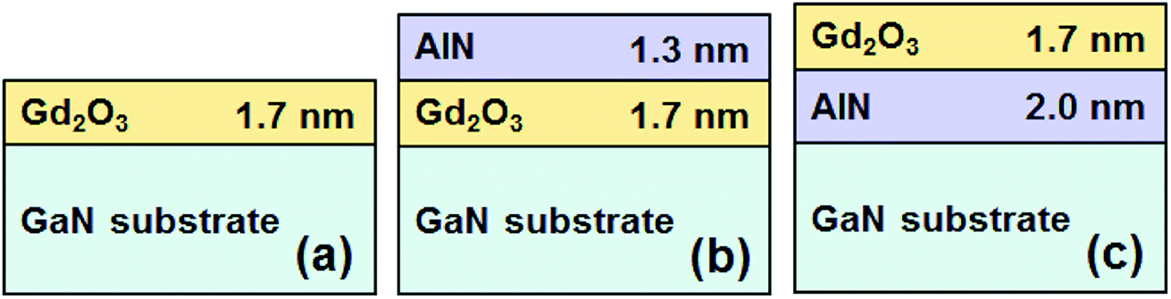 | ||
| Fig. 1 Schematic layer structures of three samples denoted as (a) Gd2O3, (b) AlN/Gd2O3 and (c) Gd2O3/AlN. | ||
3. Results and discussion
After selecting the narrow scanned XPS spectra at one etch depth (thickness of the remained AlN: ∼1.0 nm), we compared them each other to characterize the chemical reaction near the GaN surface. Fig. 2(a) shows the Ga 2p3/2 core-level spectra. The peaks at ∼1117.1, ∼1117.4, and ∼1118.1 eV are associated with Ga2O,22 Ga2O323 and GaN,24 respectively. The integrated intensity ratios of Ga–O/Ga–N were calculated to be 1.98, 0.52, and 0.38, respectively, for the samples with Gd2O3, AlN/Gd2O3 and Gd2O3/AlN layers. This indicates that the suppression of Ga–O bond occurred more significantly with a Gd2O3/AlN layer. Not Ga2O3 but Ga2O was mainly observed for the samples with AlN/Gd2O3 and Gd2O3/AlN layers, indicating that Ga2O3 transferred into Ga2O with thicker layers (so called, cleaning effect). It was shown in (In)GaAs based devices that a stable suboxide Ga2O bond at the interface were not detrimental to device characteristics and the removal of Ga2O3 resulted in the reduction of frequency dispersion in capacitance.25 As shown in Fig. 2(b), all three samples revealed a peak at ∼532.5 eV, corresponding to O in the H2O, OH− impurities26 and Gd hydroxides.27 The emission peak at 529.8–530.2 eV could be associated with O in Gd2O3,27 which became weak for the samples with AlN/Gd2O3 and Gd2O3/AlN layers. The integrated intensity ratios of [OH + O–Al]/OTotal were found to be 0.40, 0.95, and 0.95, respectively, for the samples with Gd2O3, AlN/Gd2O3 and Gd2O3/AlN layers. It was shown that Al–OH defects commonly observed in ALD-Al2O3 films is the origin of acceptor-like border traps and positive fixed charges in Al2O3.28
 | ||
| Fig. 2 XPS core level spectra of (a) Ga 2p3/2 and (b) O 1s for the samples with Gd2O3, AlN/Gd2O3 and Gd2O3/AlN layers after sputter etching. The thick of remained layer was about 1 nm. | ||
Fig. 3 shows the XPS depth profiles for each element obtained from the samples. The diffusion of Ga atoms into the overgrown layer was significant. The amount of oxygen atoms near the GaN surface is similar. However, both the samples with AlN/Gd2O3 and Gd2O3/AlN layers showed the larger amount of oxygen atoms across the overgrown layer as compared to the sample with Gd2O3 layer. This indicates that a significant portion of it resulted from the ALD deposition process itself. Fig. 4 shows the narrow scanned core level spectra from the sample surfaces (i.e., without sputter etching). As shown in Fig. 4(a), the OH related peak observed for the samples with Gd2O3 and AlN/Gd2O3 layers is not observed for the sample with a Gd2O3/AlN bilayer. Along with the relatively weak peak at ∼530.2 eV corresponding to O in Gd2O3, the additional peak at ∼528.9 eV also appeared for the samples with Gd2O3 and Gd2O3/AlN layers, which could be associated with more oxidized Gd–O due to excess O and lattice defects.29 Fig. 4(b) shows the Gd 4d core level spectra, which mainly originated from multiplet splitting of the 4d hole with 4f valence electrons to form 9D and 7D final ionic state.30 As shown in Fig. 4(c), the peak related with AlN at 73.6–73.9 eV31 is dominant for the sample with a Gd2O3/AlN bilayer whereas the peak associated with Al–O at ∼74.6 eV31 is dominant for the sample with an AlN/Gd2O3 bilayer. The additional peak at ∼75.2 eV with a Gd2O3/AlN bilayer can be conformed to the Al–O chemical bond of Al2O3 or Al(OH)3.32
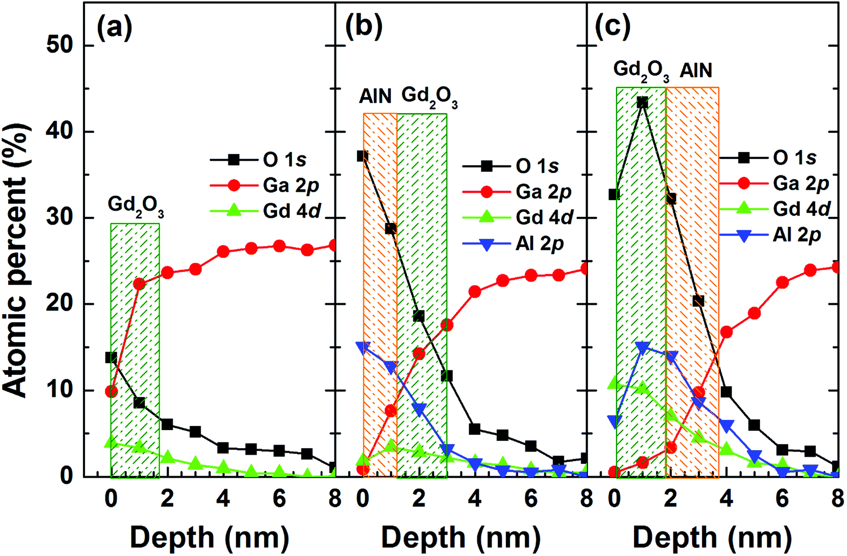 | ||
| Fig. 3 XPS depth profiles for each element for the samples with (a) Gd2O3, (b) AlN/Gd2O3 and (c) Gd2O3/AlN layers. | ||
 | ||
| Fig. 4 XPS core level spectra of (a) O 1s, (b) Gd 4d and (c) Al 2p, which were obtained from the surface. | ||
Fig. 5(a)–(c) show the C–V curves measured at 1 kHz and 1 MHz. The frequency dispersion is hardly visible in the deep depletion region and small frequency dispersion is observed in the depletion, indicating the presence of interface states. The capacitance in accumulation at 1 kHz is much higher than that at 1 MHz, which can be due to current leakage through the dielectric layer which distorts the 1 kHz measurement.33 The frequency dispersion in the accumulation region can also be associated with the formation of an inhomogeneous layer at the interface. Fig. 5(d)–(f) show the C–V hysteresis plots by sweeping the voltage from deep depletion to accumulation (up) and then accumulation to deep depletion (down). From the flatband capacitance (CFB) obtained at each voltage sweep, the flatband voltage (VFB) was calculated and then, the average interface and oxide trap density (QT) along the GaN bandgap (Eg) were obtained through QT = (COXΔVFB)/qEg.34 The trapped charge densities were calculated to be 3.68 × 10⁹, 1.82 × 10¹¹, and 1.83 × 1012 cm−2 eV−1, respectively, for the samples with Gd2O3, AlN/Gd2O3, and Gd2O3/AlN layers. The hysteresis can result from the interface states and oxide traps in the dielectric layer. Oxygen related defects are generated much with including an AlN layer (for example, see Fig. 2(b)). High density of Al–OH defects acting as acceptor-like border traps and positive fixed charges in Al2O3 may also increase the VFB shift. Fig. 5(f) also shows that the C–V curves reveal a plateau region, reflecting the presence of 2 dimensional electron gas (2DEG) at the AlN/GaN interface.35,36 With increasing the bias voltage, electrons start to accumulate at the channel interface, thus forming the 2DEG. An increase in capacitance is also observed at gate bias beyond +5 V. This is due to a charge spillover from the 2DEG channel, which brings some of the carriers closer to the surface, decreasing the effective barrier layer thickness and increasing the capacitance.37
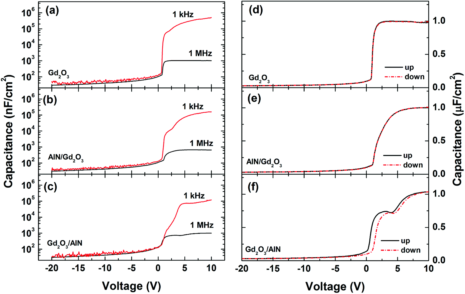 | ||
| Fig. 5 (a)–(c) Capacitance–voltage (C–V) data measured at 1 kHz and 1 MHz and (d)–(f) C–V hysteresis plots measured at 1 MHz. | ||
Frequency dependent conductance–voltage measurements were performed to differentiate the types of the traps. The parallel conductance (Gp/ω) can be derived by Gp/ω = [ωGm(COX)2]/[(Gm)2 + ω2(COX − Cm)2], where Cm is the measured capacitance, Gm is the measured conductance, and COX is the oxide capacitance. The Gp/ω values as a function of radial frequency (ω = 2πf) can be correlated with the trap density DT and trap response time τT, given by38
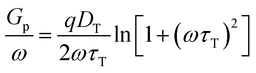 | (1) |
The experimental and fitting data are shown in Fig. 6(a)–(c). The energy level of traps below the GaN conduction band, denoted as EC–Et (location of the trap energy) can be determined from τT according to the Shockley–Read–Hall statistics39,40
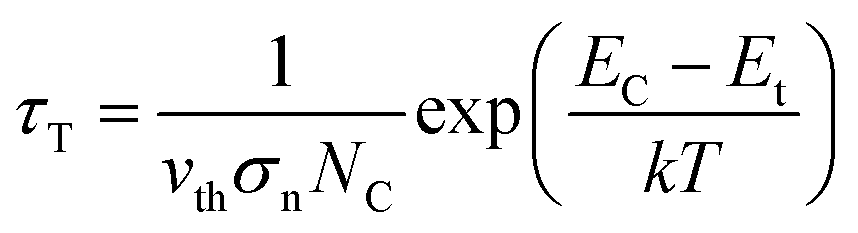 | (2) |
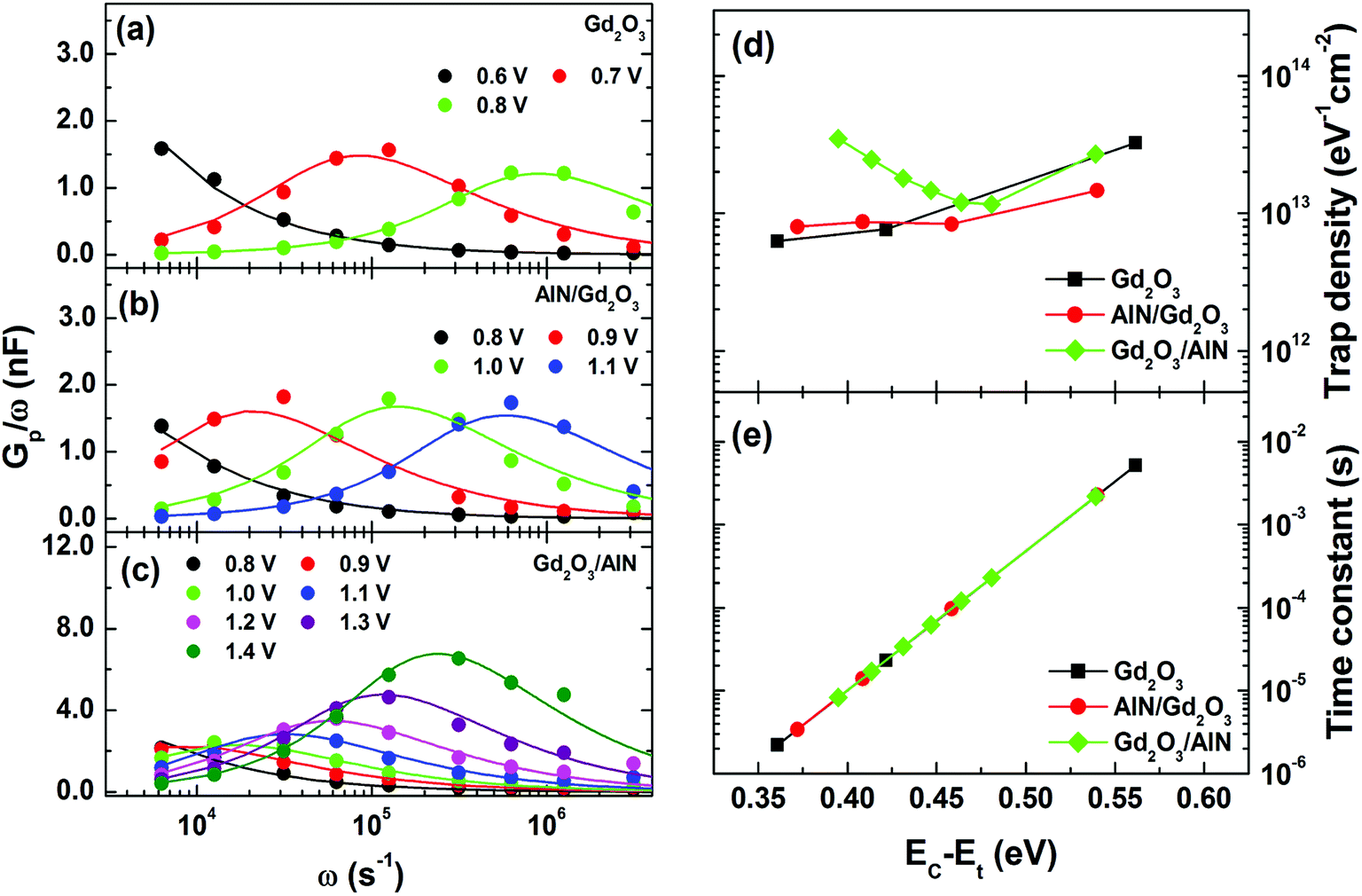 | ||
| Fig. 6 Frequency dependent parallel conductance for the samples with (a) Gd2O3, (b) AlN/Gd2O3 and (c) Gd2O3/AlN, and (d) the obtained trap density and (e) the time constant from the conductance method. | ||
As shown in Fig. 7(a), an estimate of the interface state density (Dit) was made by applying Terman method to the experimental C–V curves measured at 1 MHz.38 The obtained Dit vs. EC–Et plots in Fig. 7(b) revealed the lowest interface state density for the sample with a Gd2O3 layer. Interestingly, the samples with AlN/Gd2O3 and Gd2O3/AlN bilayers showed the highest interface state densities in the energy ranges of 0.1–0.2 eV and 0.4–0.6 eV, respectively. As shown in Fig. 3, large amount of Al atoms are present near the Gd2O3/GaN interface for the sample with an AlN/Gd2O3 bilayer. This might lead to the formation of AlN, leaving many nitrogen vacancies at the GaN surface. Fang et al. reported that several kinds of deep levels can be increased at the GaN surface after Cl2-based inductively coupled plasma (ICP) etching.41 In particular, they attributed a deep center located at EC – 0.17 eV to nitrogen vacancy-related defect due to ICP etching. Yatabe et al. also showed in Al2O3/AlGaN/GaN structure that the C–V curves in the depletion region are stretched out more significantly to the positive direction when the interface state density peaked at EC – 0.1 eV is higher.42 Significant stretch out to the positive direction and high interface state density in the range of 0.1–0.2 eV observed for the sample with an AlN/Gd2O3 bilayer, thus, can be associated with the nitrogen vacancy-related defects. Meanwhile, Freedsman et al. showed in AlN/AlGaN/GaN MIS diodes that the trap density due to the AlN and AlGaN layers were located at 0.4–0.52 and 0.32–0.34 eV, respectively.43 The energy distribution corresponding to the AlN insulating layer is similar to our work at the Gd2O3/AlN interface. Furthermore, Fig. 7(a) shows that flatband voltage shifted negatively for the sample with a Gd2O3 layer as compared to the sample with an AlN/Gd2O3 bilayer. It was shown that when Gd can only exist in the +3 oxidation state, the Gd2O3 cannot supply oxygen effectively to the dielectric/Si interface, which produced oxygen vacancies causing the negative shift in flatband voltage.44 As shown in Fig. 2(b), the strong Gd2O3 related emission observed for the sample with a Gd2O3 layer was not observed for the sample with an AlN/Gd2O3 bilayer. Instead, the emission related with more oxidized Gd–O bond was observed. Therefore, it can be expected that oxygen vacancies have been reduced after depositing AlN layer with the excess O atoms.
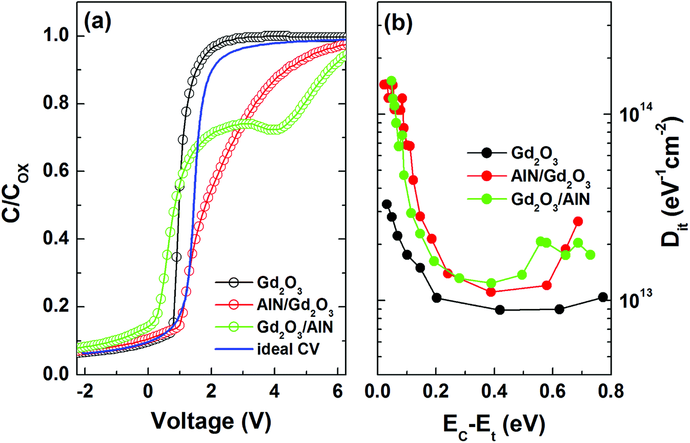 | ||
| Fig. 7 (a) Comparison of experimental capacitance–voltage (C–V) data measured at 1 MHz and ideal C–V data and (b) interface state density (Dit) distributions determined by applying Terman method. | ||
Fig. 8(a) shows the typical semi-logarithmic current density–voltage (J–V) curves measured at room temperature. Compared to the sample with a Gd2O3 layer, the reverse leakage current increased for the samples with AlN/Gd2O3 and Gd2O3/AlN layers. Forward current at high bias region increased most slowly for the sample with a Gd2O3/AlN bilayer, indicating the high series resistance. The reverse leakage current density at high bias region were analyzed using the Fowler–Nordheim (FN) tunneling model, given by45
|
J ∝ E2exp(−β/E)
| (3) |
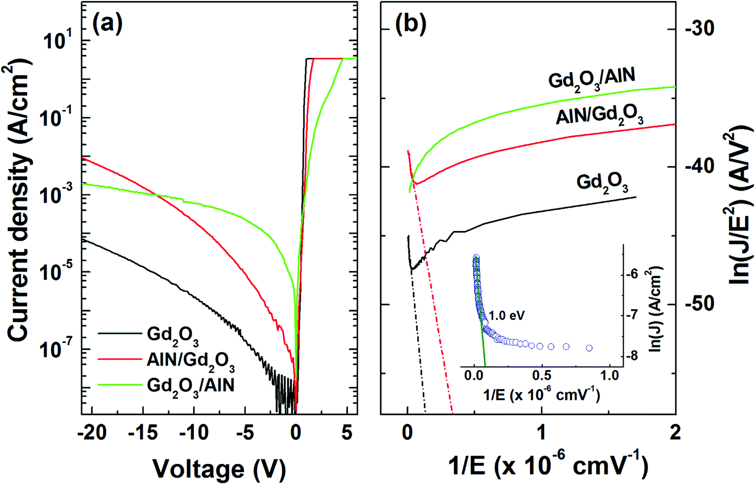 | ||
| Fig. 8 (a) Typical semi-logarithmic current density–voltage (J–V) characteristics and (b) Fowler–Nordheim (FN) tunneling plots of ln(J/E2) vs. 1/E. The inset in (b) presents trap assisted tunneling (TAT) plot of ln(J) vs. 1/E. | ||
Fig. 8(b) also shows that no FN emission was observed for the sample with a Gd2O3/AlN bilayer. Instead of FN emission, the trap assisted tunneling (TAT) was applied to the sample with a Gd2O3/AlN bilayer. In TAT emission, the reverse leakage current is given as J ∝ exp(−γ/E), where γ = 6.83 × 10⁻⁷(m*)1/2(Φt)3/2 and Φt is the trap energy level, which can be obtained from the ln(J) vs. 1/E plot. From the linear fittings to the data as shown in the inset in Fig. 8(b), the trap energy level was estimated to be 1.00 eV. Energetically most favorable point defects in AlN are substitutional oxygen for nitrogen (ON) and aluminum vacancy (VAl), with the energy levels of ∼0.8 and ∼1.0 eV, respectively.47 It was shown that dangling bonds in Al give rise to ∼1.0 eV in energy level.48 At present moment, it is suggested that Al related defects are responsible for TAT emission for the sample with a Gd2O3/AlN bilayer.
4. Conclusions
In conclusion, we investigated the interfacial and electrical properties of atomic layer deposited Gd2O3 with an AlN layer on n-GaN. X-ray photoelectron spectroscopy (XPS) spectra showed the dominant peaks associated with Ga–O and O–Al bonds, respectively, near the Gd2O3/GaN and AlN/Gd2O3/GaN and Gd2O3/AlN/GaN interfaces. Large amount of oxygen atoms across the dielectric layers were observed for the samples with Gd2O3/AlN and AlN/Gd2O3 layers. The highest flatband voltage shift in C–V hysteresis characteristics were observed for the sample with a Gd2O3/AlN bilayer, indicating the highest interface and oxide trap densities. According to parallel conductance and Terman methods, the samples with AlN/Gd2O3 and Gd2O3/AlN layers were found to have the highest interface state densities in the energy ranges of 0.1–0.2 eV and 0.4–0.6 eV, respectively. The reverse leakage currents for the samples with Gd2O3 and AlN/Gd2O3 layers were explained by Fowler–Nordheim (FN) whereas trap assisted tunneling (TAT) was more appropriate for the sample with a Gd2O3/AlN bilayer.Conflicts of interest
There are no conflicts to declare.Acknowledgements
This work was supported by Basic Science Research Program through the National Research Foundation of Korea (NRF) funded by the Ministry of Education (2017R1D1A1B03030400).References
- A. Laha, H. Osten and A. Fissel, Appl. Phys. Lett., 2006, 89, 143514 CrossRef.
- H. Gottlob, T. Echtermeyer, M. Schmidt, T. Mollenhauer, J. Efavi, T. Wahlbrink, M. Lemme, M. Czernohorsky, E. Bugiel, A. Fissel, H. Osten and H. Kurz, IEEE Electron Device Lett., 2006, 27, 814 CAS.
- K. Kukli, T. Hatanpää, M. Ritala and M. Leskelä, Chem. Vap. Deposition, 2007, 13, 546 CrossRef CAS.
- V. Afanas'ev and A. Stesmans, Mater. Sci. Semicond. Process., 2006, 9, 764 CrossRef.
- P. Yang, P. Ye, J. Kwo, M. Frei, J. Gossmann, J. Mannaerts, A. Sergent, M. Hong, K. Ng and J. Bude, J. Cryst. Growth, 2003, 251, 837 CrossRef.
- K. Xu, R. Ranjith, A. Laha, H. Parala, A. Milanov, R. Fischer, E. Bugiel, J. Feydt, S. Irsen, T. Toader, C. Bock, D. Rogalla, H. Osten, U. Kunze and A. Devi, Chem. Mater., 2012, 24, 651 CrossRef CAS.
- X. Hu, A. Koudymov, G. Simin, J. Yang, M. Asif Khan, A. Tarakji, M. Shur and R. Gaska, Appl. Phys. Lett., 2001, 79, 2832 CrossRef CAS.
- T. Hashizume, S. Ootomo and H. Hasegawa, Appl. Phys. Lett., 2003, 83, 2952 CrossRef CAS.
- J. Shi, L. Eastman, X. Xin and M. Pophristic, Appl. Phys. Lett., 2009, 95, 042103 CrossRef.
- C. Mizue, Y. Hori, M. Miczek and T. Hashizume, Jpn. J. Appl. Phys., 2011, 50, 021001 CrossRef.
- S. Huang, S. Yang, J. Roberts and K. Chen, Jpn. J. Appl. Phys., 2011, 50, 110202 CrossRef.
- S. Huang, Q. Jiang, S. Yang, C. Zhou and K. Chen, IEEE Electron Device Lett., 2012, 33, 516 CAS.
- S. Huang, Q. Jiang, S. Yang, Z. Tang and K. Chen, IEEE Electron Device Lett., 2013, 34, 193 CAS.
- S. Zhao, X. Liu, L. Zhang, H. Huang, J. Shi and P. Wang, Nanoscale Res. Lett., 2016, 11, 137 CrossRef PubMed.
- Q. Luc, E. Chang, H. Trinh, Y. Lin, H. Nguyen, Y. Wong, H. Do, S. Salahuddin and C. Hu, IEEE Trans. Electron Devices, 2014, 61, 2774 CAS.
- Q. Luc, H. Do, M. Ha, C. Hu, Y. Lin and E. Chang, IEEE Electron Device Lett., 2015, 36, 1277 CAS.
- X. Wu, R. Liang, L. Guo, L. Lei, L. Xiao, S. Shen, J. Xu and J. Wang, Appl. Phys. Lett., 2016, 109, 232101 CrossRef.
- H. Kim, D. Kim and B. Choi, Appl. Phys. A, 2017, 123, 800 CrossRef.
- H. Kim, H. Yoon and B. Choi, Nanoscale Res. Lett., 2018, 13, 232 CrossRef.
- W. Chang, P. Chang, T. Lai, Y. Lee, J. Kwo, C. Hsu and M. Hong, Cryst. Growth Des., 2010, 10, 5117 CrossRef CAS.
- J. Johnson, B. Luo, F. Ren, B. Gila, W. Krishnamoorthy, C. Abernathy, S. Pearton, J. Chyi, T. Nee, C. Lee and C. Chuo, Appl. Phys. Lett., 2000, 77, 3230 CrossRef CAS.
- S. Wolter, B. Luther, D. Waltemyer, C. Önneby, S. Mohney and R. Molnar, Appl. Phys. Lett., 1997, 70, 2156 CrossRef CAS.
- F. Wang, K. Chen, C. Hsu, M. Liu and C. Yang, Nanomaterials, 2016, 6, 88 CrossRef.
- C. Hinkle, E. Vogel, P. Ye and R. Wallace, Curr. Opin. Solid State Mater. Sci., 2011, 15, 188 CrossRef CAS.
- C. Hinkle, M. Milojevic, B. Brennan, A. Sonnet, F. Aguirre-Tostado, G. Hughes, E. Vogel and R. Wallace, Appl. Phys. Lett., 2009, 94, 162101 CrossRef.
- M. Li, D. Gao, S. Li, Z. Zhou, J. Zou, H. Tao, L. Wang, M. Xu and J. Peng, RSC Adv., 2015, 5, 104613 RSC.
- S. Jeon and H. Hwang, J. Appl. Phys., 2003, 93, 6393 CrossRef CAS.
- J. Raja, C. Nguyen, C. Lee, N. Balaji, S. Chatterjee, K. Jang, H. Kim and J. Yi, IEEE Electron Device Lett., 2016, 37, 1272 CAS.
- E. Külah1, L. Marot, R. Steiner, A. Romanyuk, T. Jung, A. Wäckerlin and E. Meyer, Sci. Rep., 2017, 7, 43369 CrossRef PubMed.
- J. Gupta, D. Landheer, J. McCaffrey and G. Sproule, Appl. Phys. Lett., 2001, 78, 1718 CrossRef CAS.
- M. Alevli, C. Ozgit, I. Donmez and N. Biyikli, Phys. Status Solidi A, 2009, 2, 266 Search PubMed.
- B. Brennan, R. Galatage, K. Thomas, E. Pelucchi, P. Hurley, J. Kim, C. Hinkle, E. Vogel and R. Wallace, J. Appl. Phys., 2013, 114, 104103 CrossRef.
- R. Khosa, E. Thorsteinsson, M. Winters, N. Rorsman, R. Karhu, J. Hassan and E. Sveinbjörnsson, AIP Adv., 2018, 8, 025304 CrossRef.
- C. Lee, H. Chen and H. Lee, Appl. Phys. Lett., 2003, 82, 4304 CrossRef CAS.
- M. Fagerlind, F. Allerstam, E. Sveinbjörnsson, N. Rorsman, A. Kakanakova-Georgieva, A. Lundskog, U. Forsberg and E. Janzén, J. Appl. Phys., 2010, 108, 014508 CrossRef.
- T. Hashizume, S. Ootomo, T. Inagaki and H. Hasegawa, J. Vac. Sci. Technol., B: Microelectron. Nanometer Struct.--Process., Meas., Phenom., 2003, 21, 1828 CrossRef CAS.
- D. Cao, X. Cheng, Y. Xie, L. Zheng, Z. Wang, X. Yu, J. Wang, D. Shen and Y. Yu, RSC Adv., 2015, 5, 37881 RSC.
- E. Nicollian and J. Brews, MOS Physics and Technology, John Wiley & Sons, New York, 1982 Search PubMed.
- D. Schroder, Semiconductor Material and Device Characterization, Wiley, New York, 2005 Search PubMed.
- S. Liu, S. Yang, Z. Tang, Q. Jiang, C. Liu, M. Wang, B. Shen and K. Chen, Appl. Phys. Lett., 2015, 106, 051605 CrossRef.
- Z. Fang, D. Look, X. Wang, J. Han, F. Khan and I. Adesida, Appl. Phys. Lett., 2003, 82, 1562 CrossRef CAS.
- Z. Yatabe, J. Asubar, T. Sato and T. Hashizume, Phys. Status Solidi A, 2015, 212, 1075 CrossRef CAS.
- J. Freedsman, T. Kubo and T. Egawa, Appl. Phys. Lett., 2011, 99, 033504 CrossRef.
- S. Dueñas, H. Castán, H. García, A. Gómez, L. Bailón, K. Kukli, T. Hatanpää, J. Lu, M. Ritala and M. Leskelä, J. Electrochem. Soc., 2007, 154, G207 CrossRef.
- H. Lin, P. Ye and G. Wilk, Appl. Phys. Lett., 2005, 87, 182904 CrossRef.
- J. Robertson and B. Falabretti, J. Appl. Phys., 2006, 100, 014111 CrossRef.
- C. Stampfl and C. van de Walle, Phys. Rev. B, 2002, 65, 1 Search PubMed.
- C. Wu and A. Kahn, Appl. Phys. Lett., 1999, 74, 546 CrossRef CAS.
| This journal is © The Royal Society of Chemistry 2018 |