
 Open Access Article
 This Open Access Article is licensed under a Creative Commons Attribution-Non Commercial 3.0 Unported Licence
Facile synthesis of AgBiS2 nanocrystals for high responsivity infrared detectors†
Chun Hin Mak,
Jiasheng Qian,
Lukas Rogée,
Wai Kin Lai and
Shu Ping Lau *
*
Department of Applied Physics, The Hong Kong Polytechnic University, Hung Hom, Kowloon, Hong Kong SAR. E-mail: apsplau@polyu.edu.hk
First published on 23rd November 2018
Abstract
AgBiS2 nanocrystals are emerging optoelectronic materials due to their solution-processability, earth abundance and non-toxic properties. We report a facile method to prepare AgBiS2 nanocrystals in ambient conditions. The nanocrystals are of high crystallinity and without byproducts, which make them suitable for solution processable optoelectronic devices. They were incorporated into graphene transistors for their near infrared detection application. Photodetectors with a high photo-responsivity of 105 A W−1 for 895 nm wavelength at a low operation voltage of 0.1 V were demonstrated.
Introduction
Over the past decade, lead chalcogenide nanocrystals (NCs) such as lead sulphide (PbS) have been intensively studied for solar cells and infrared (IR) detection.1–6 Due to their high absorption coefficients and solution dispersibilities, high performance solar cells and hybrid phototransistors have been demonstrated. However, the toxicity of lead causes long term environmental and biological issues,7 which limits its applications. Recently, AgBiS2 NCs, as a non-toxic and high stability material, have been utilized as the active material for solar cells showing a power conversion efficiency of 6.3%.8 The work was recognized as the first demonstration of efficient inorganic nanocrystal-based solar cells which simultaneously fulfilled the advantages of non-toxicity, abundance, low-temperature and solution processability. However, even though the AgBiS2 NCs exhibited a high infrared external quantum efficiency in the aforementioned solar cells with a bandgap fall in the infrared region (1.0–1.25 eV),8,9 the investigation in near infrared (NIR) detection is scarce.Graphene transistors have been used for IR detection but the responsivity is very low (<10 mA W−1).10–12 This is due to the low optical absorption of graphene,13,14 which makes graphene transistor not favourable for photodetection. Graphene itself, however, provides a high mobility for charge carriers.15 Therefore graphene transistor has been hybridized with various semiconducting NCs such as PbS and halide perovskite (CsPbX3) for broad range photodetection.16,17 The photo-responsivities of PbS and CsPbX3 based graphene transistors could reach 107 and 108 A W−1 respectively. Recently another non-toxic Si NCs was hybridized with graphene and showed a photo-responsivity of 108 to 109A W−1 under 375 nm to 1870 nm light illumination. The devices also exhibited mid-infrared photo-responsivity of 0.22–44.9 A W−1 in 2.5 to 3.9 μm.18 Both works evidence that graphene transistor is an ideal platform to amplify the intrinsic optoelectronic properties of the NCs.
It is also favorable that the synthesis of functional NCs becomes simple and cost effective. Herein we present a facile synthetic route for AgBiS2 NCs with a much shorter processing time under ambient conditions as compared to the conventional hot injection method.8 The AgBiS2 NC solution was spin-coated onto a graphene transistor for 895 nm light detection. A high photo-responsivity of 1.24 × 10⁵ A W−1 was achieved by a small operation voltage of VDS = 0.1 V. Our findings demonstrate that the AgBiS2 NCs can be synthesized by a facile technique for optoelectronic application.
Experimental
Chemicals and reagents
Oleic acid (OA), octanoic acid (OctA), octylamine (OTA), dodecylamine (DDA), tetrabutylammonium iodide (TBAI) and sulfur powder were purchased from Sigma Aldrich. Silver nitride (AgNO3) and bismuth(III) nitrate pentahydrate (Bi(NO3)3·5H2O) were purchased from Aladdin. Toluene, methanol and ethanol were ACS reagent grade. All chemicals were used without any purification.Materials synthesis
Typically, 0.1 mmol AgNO3 and 0.1 mmol Bi(NO3)3·5H2O were heated (120 °C) and stirred by a heating mantle in a flask containing 10 mL oleic OA (or OctA) until fully dissolved and the color turned pale yellow. Then 0.1 mmol sulfur powder was dissolved and stirred into a long chain length amine such as OTA (or DDA). After the dissolution of all the precursors, 1 mL Ag/Bi and 1 mL sulfur were mixed under vigorous stirring in room temperature and atmosphere. The color of the whole mixture turned black immediately and the AgBiS2 nanocrystals were formed. After the synthesis process, the AgBiS2 nanocrystals were washed by precipitation/dispersion in a toluene/ethanol mixture via centrifugation. The AgBiS2 NCs were dispersed in toluene after washing three times.Graphene was prepared by using a 2-inch copper foil (Alfa Aesar, 0.025 mm thick) in a plasma enhanced chemical vapor deposition chamber (Aixtron CVD). The synthesis process of graphene included the following steps: the Cu foil was annealed in a mixture gas (Ar: 250 sccm, Ar/H2: 1000 sccm) at constant pressure of 25 mbar. The annealing process was carried out at 1020 °C for 15 minutes. Then methane gas (15 sccm) was injected into the chamber. The graphene formation was lasted for 5 minutes. Finally, the sample was cooled down to 150 °C under Ar flow.
Device fabrication and electrical measurement
First of all, Cr/Au metal electrodes were patterned on Si/SiO2 substrate (SiO2, 300 nm thick) by photolithography and then DC magnetron sputtering deposition. A thin layer of poly(methyl methacrylate) (PMMA) was spun-coated on top of graphene/copper foil and heated at 150 °C for 30 minutes. Then the PMMA/graphene/copper composite was let to float on ammonium persulfate/deionized water solution with concentration 2 g/60 mL. After the copper foil was completely etched, the PMMA/graphene composite was cleaned with DI water for two times and transferred onto the patterned Cr/Au electrodes and dried at 120 °C for 30 minutes. Finally, the samples were immersed into acetone for 6 hours to remove PMMA and the graphene transistor was ready for use.For AgBiS2/graphene hybrid, AgBiS2 NCs were dropped onto the graphene transistor and spin-coated with 2000 rpm for 30 s. Then, 5 mg mL−1 TBAI/methanol solution was drop onto the AgBiS2 NCs to replace the long organic ligand to single atom ligand iodine, then spin-coated with 2000 rpm for 30 s. The device was rinsed with methanol followed by toluene. The above procedure is for a cycle of layer-by-layer (LBL) AgBiS2 deposition. The AgBiS2 NCs were deposited by 5 (5-layer) and 10 (10-layer) cycles of LBL deposition respectively. The thickness of the AgBiS2 film for 10 cycles deposition is about 72 nm. The transistors were annealed at 150 °C for 90 minutes in a N2-filled glove box to remove the surface adsorbates.
All the electrical measurements for both the control graphene transistor and the AgBiS2/graphene transistor were carried out with a Keithley 4200-SCS at room temperature in a nitrogen filled glove box with O2, H2O < 10 ppm. For infrared detection, a light emitting diode with emission wavelength of 895 nm was used to illuminate the transistor channel.
Materials characterization
Transmission electron microscopy (TEM), selected area electron diffraction (SAED) and energy-dispersive X-ray spectroscopy (EDX) measurements were performed by JEOL Model JEM-2100F Field Emission Electron Microscope STEM. Carbon coated copper grids were used as X-ray diffraction (XRD) measurement was conducted by the Rigaku SmartLab X-ray Diffractometer. Cross-sectional image of the AgBiS2 thickness was observed by Tescan VEGA3 Scanning Electron Microscope. Raman spectrum of graphene was measured by LabRAM HR 800 Raman Spectrometer. Fourier Transform Infrared (FTIR) spectroscopy of the NCs on quartz was obtained by The Bruker Vertex-70 FTIR.Results and discussion
In our experiment, 0.1 mM Ag/Bi oleate solution and 0.2 mM sulfur amine solution were mixed under rigorous stirring, resulting to a black solution. Fig. 1A shows the photograph of the three solutions and revealing their colours. Besides the OA and DDA ligand pair used, two other pairs namely OA and OTA, OctA and OTA, were also employed to fabricate the NCs with similar result. Detailed synthesis information is described in the materials synthesis section.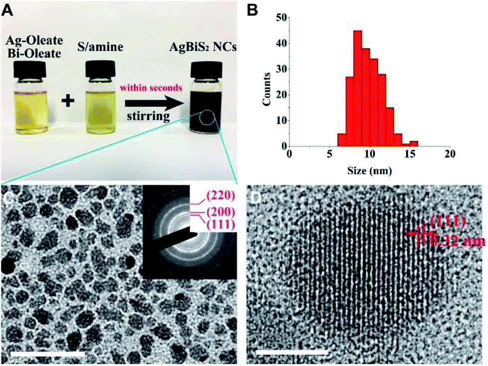 | ||
| Fig. 1 Characterizations of the AgBiS2 NCs synthesized by OA/DDA. (A) Photograph of the Ag/Bi-oleate, sulfur in amine and the AgBiS2 NCs. (B) Size distribution profile of the AgBiS2 NCs. (C) TEM image of the AgBiS2 NCs. Scale bar is 50 nm. Inset: SAED pattern. (D) High resolution TEM image of a single AgBiS2 NC. Scale bar is 5 nm. | ||
TEM was used to characterize the size distribution and crystal structure of the NCs produced by the OA/DDA ligand. The size distribution of the NCs is ranging from 7 to 15 nm with the most frequent size at around 8 nm as shown in Fig. 1B. TEM image and SAED pattern in Fig. 1C depict that the NCs are having a cubic structure. SAED pattern shows clear rings of the (111), (200), and (220) crystal planes. The results are in good agreement with the XRD pattern of the sample, revealing three major peaks corresponding to the plane (111), (200), and (220) of AgBiS2 as shown in Fig. S1.† Fig. 1D shows the high resolution TEM image of a single NC revealing the interplanar distance of 0.32 nm for the atomic plane of (111). The composition of the product was analysed by EDX. The result reveals that the atomic ratio of Ag/Bi/S is very close to 1![[thin space (1/6-em)]](https://www.rsc.org/images/entities/char_2009.gif) :1:2 and no oxygen is detected. Similar characterization results were obtained when the ligand pairs changed to OA/OTA and OctA/OTA (Fig. S2 and S3†). The result indicates that the choice of the ligand – pair is independent on the synthesis process.
:1:2 and no oxygen is detected. Similar characterization results were obtained when the ligand pairs changed to OA/OTA and OctA/OTA (Fig. S2 and S3†). The result indicates that the choice of the ligand – pair is independent on the synthesis process.
Cubic AgBiS2 was reported to have the bandgap of about 0.8 eV in the bulk form and about 1.0–1.25 eV in the nanocrystalline form.8,9 Fig. 2A shows the absorption spectrum of the NCs in toluene, revealing a broad absorption covering 400 nm to 1000 nm. The graphene was prepared by chemical vapor deposition and characterized by Raman scattering. The graphene is monolayer and no defect peaks was found (Fig. S4†). The intrinsic transfer characteristic curve from −80 V to 80 V was characterized before the deposition of the NCs (Fig. S5†). The Dirac point is located at 5 V which indicates a slight p-type characteristic. It is noteworthy that the long aliphatic chain molecule ligands such as OA/DDA are insulating which inhibits the charge transfer through the NCs to the surrounding.19,20 Therefore, the surface ligand exchange was changed to iodide ligand to enhance the surface's conductivity. Fourier-transform infrared spectroscopy (FTIR) was measured on the samples before and after the ligand exchange. Fig. 2B shows the transmittance spectra of the AgBiS2 NCs on a quartz substrate before and after the ligand exchange. The C–H vibrations (2922 cm−1 and 2852 cm−1) are nearly disappeared after the ligand exchange, which implies the removal of the long aliphatic chain ligand OA/DDA from the NCs surface.2,21
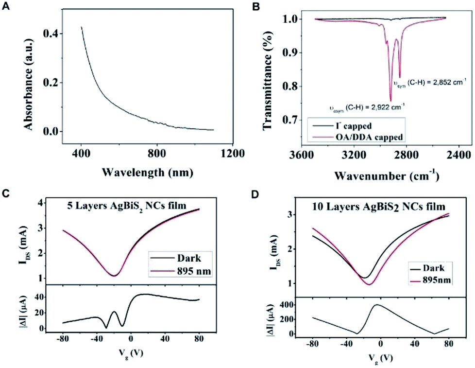 | ||
| Fig. 2 (A) UV-vis absorption spectrum of AgBiS2 NCs in toluene. (B) The FTIR spectra of the films before (OA/DDA capped) and after (I-capped) solid state ligand exchange. (C and D) The transfer characteristic curves with/without 895 nm light illumination (UP) and photocurrent change (down) for the hybrid transistor with 5 layers NC film (C) and 10 layers NC film (D), illumination intensity = 10.43 mW cm−2. | ||
The layer-by-layer deposition was employed to deposit the NC film and exchange the ligands to provide different thicknesses of the AgBiS2 films on the transistors.8 We prepared two graphene transistors with 5-layer (5L) and 10-layer (10L) NC films. According to the SEM measurement, the film thickness of the 10L sample is about 72 nm (Fig. S6†). Fig. 2C and D show the transfer characteristic curves of the 5L and 10L devices with and without 895 nm light illumination. An applied voltage of 0.1 V (i.e. VDS = 0.1 V) was applied to the drain and source electrodes. The Dirac point of the 5L and 10L devices are in the negative voltage region and indicating their n-type characteristic. Under light illumination, the Dirac point of 10L device is obviously shifted to the positive voltage side which indicates a net hole doping to the graphene channel. As the quantity of the main charge carrier electron is reduced, the decrease in current are resulted. As an evidence, the currents under illumination in Fig. 2C and D at Vg = 0 V are also decreased as compared to the dark current. The absolute photocurrent of these devices was calculated by subtracting of the current of the illuminated and unilluminated devices. The high absolute photocurrents values around Vg = 0 V were observed in both devices. Therefore the photo-responsivity measurement was characterized at Vg = 0 V and VDS = 0.1 V.
Fig. 3 shows the temporal photo-response of the 5L and 10L devices under an intensity of 12.28 μW cm−2. The response time and current change are highly repeatable for both devices. The current change is about 1 μA for the 5L device and about 20 μA for the 10L device (Fig. 3A and C, respectively). The response time of the 5L device is 2.62 s, which is nearly twice of the recovery time (Fig. 3B). In addition, the response time becomes longer when increasing the NC film thickness. The response time of the 5L device is 9 s, while the recovery time is 29 s (Fig. 3D). The results clearly demonstrate that under the same light intensity illumination, the thicker absorber film will lead to higher photocurrent change but longer stabilization time for response and recovery, vice versa.
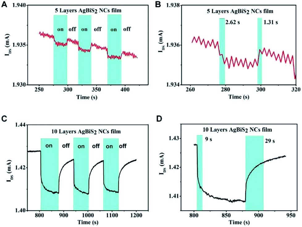 | ||
| Fig. 3 (A) The photocurrent response of the 5L device. (B) Reaction time and recovery time of the 5L device. (C) The photocurrent response of the 10L device. (D) Reaction time and recover time of the 10L device. The light intensity of 12.28 μW cm−2 was used for all the measurements. | ||
To illustrate the difference of stabilization time, the schematic diagram of charge transfer mechanism is shown in Fig. 4. When the light illuminates the graphene transistors, electron–hole pairs (EHPs) are generated and holes are transferred to the graphene channel (Fig. 4B). This results in the decrease of Fermi level in the graphene, leading to positive shift of the Dirac point. According to the photo-gating effect, the holes will be accumulated in the graphene channel while electrons are trapped into the AgBiS2 NC film. Since the transistors were annealed and characterized in N2-filled glovebox, the surface adsorbates such as moisture and oxygen were removed as much as possible. So the trapping of charge carriers are likely come from the surface defects of the NCs.5,18,22 Under light illumination, the current is changing with the increasing holes concentration in the graphene until equilibrium is reached.22,23 However, the holes at the graphene channel generate an opposing electric field to the absorber and hinder the rate of holes injection. As a result, the response time will be increased. Considering the thickness dependent light absorption of the absorber, fewer holes are generated from the NC film under illumination for the 5L device due to weaker absorption. Fewer holes will be injected to the graphene and weaken the opposing field as compared with the 10L device. When the light is off, the trapped electrons are released and recombined with the holes. The 10L device's have thicker NC film and hence it trapped more electrons than the 5L device. The total time of releasing the electrons is longer in the 10L device as compared to the 5L one. Consequently the temporal photo-response and recovery time of the 5L device is faster than the 10L device, but the photocurrent change is smaller than the 10L device.24
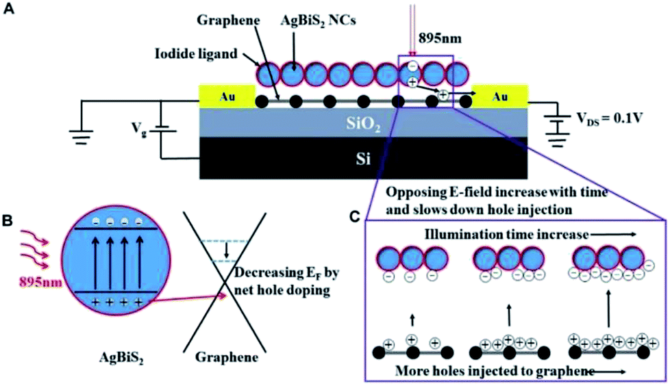 | ||
| Fig. 4 (A) The schematic illustration of the AgBiS2 NCs/graphene photodetector. The wavelength of light is 895 nm. (B) The schematic diagram for charge generation at the AgBiS2 NCs/graphene heterojunction under illumination. (C) The schematic diagram for opposing field at the AgBiS2 NCs/graphene heterojunction, thicker film usually lead to a longer response time and stabilization time. | ||
The photo-responsivity R is defined as the output photocurrent Iph divided by the incident light power Pin,22,23 i.e.
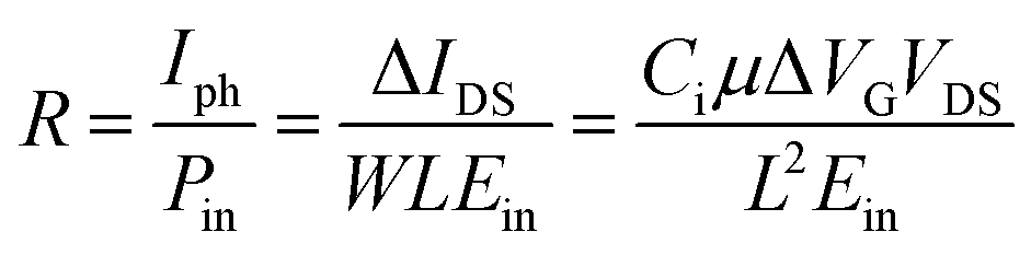 | (1) |
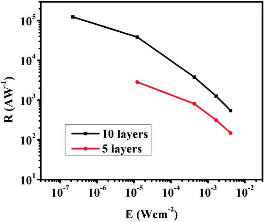 | ||
| Fig. 5 Photo-responsivities of the 5L and 10L devices under 895 nm illumination. | ||
| Channel materials (atomic layers) | Absorber and thickness | Wavelength/lowest detection | Operating voltage VDS (V) | Responsivity (A W−1) | R/VDS (A W−1 V−1) | Ref. |
|---|---|---|---|---|---|---|
| a ME: mechanical exfoliation, CVD: chemical vapor deposition, EDT: ethanedithiol. | ||||||
| ME graphene (1–2 layers) | 60–80 nm PbS QDs in EDT | 600 nm/8 fW | 5 | 4 × 10⁷ | 8 × 10⁶ | 5 |
| ME SnS2 (5 layers) | PbS QDs in EDT | 400–1000 nm/∼10 nW cm−2 | 1 | 1 × 10⁶ | 1 × 10⁶ | 6 |
| ME MoS2 (≥2 layers) | 40–60 nm PbS QDs in EDT | 400–1500 nm/3 μW cm−2 | 1 | 6 × 10⁵ | 6 × 10⁵ | 3 |
| CVD WS2 (1 layer) | 87.8 nm PbS QDs in EDT | 808 nm/about 0.2 mW cm−2 | 1.5 | 14 | 9.3 | 25 |
| CVD graphene (1 layer) | 105 nm Si NCs | 375–1870 nm/about 0.2 μW cm−2 | 1 | 1.2 × 10⁸ to 2.2 × 10⁹ | 1.2 × 10⁸ to 2.2 × 10⁹ | 18 |
| CVD graphene (1 layer) | 72 nm AgBiS2 NCs in iodide | 895 nm/8.86 pW | 0.1 | 1.24 × 10⁵ | 1.24 × 10⁶ | This work |
Conclusions
In summary, we have successfully synthesized AgBiS2 NCs in an ambient environment without any observable by-products or oxide content. The NCs are highly dispersive in toluene which makes the NCs solution very suitable for solution processable device. The AgBiS2 NCs was introduced to the graphene transistor, which showed high responsivity of 103 to 105 A W−1 with infrared illumination.Conflicts of interest
There are no conflicts to declare.Acknowledgements
CHM acknowledges the support of the Hong Kong PhD Fellowships scheme. This work was financially supported by and PolyU grants (Project no. 4-BCAK and 1-ZVGH). The authors acknowledge Dr Cao Xie and Prof. Feng Yan for device characterization.References
- R. Saran and R. J. Curry, Nat. Photonics, 2016, 10, 81 CrossRef CAS.
- Y. Cao, A. Stavrinadis, T. Lasanta, D. So and G. Konstantatos, Nat. Energy, 2016, 1, 16035 CrossRef CAS.
- D. Kufer, I. Nikitskiy, T. Lasanta, G. Navickaite, F. H. Koppens and G. Konstantatos, Adv. Mater., 2015, 27, 176–180 CrossRef CAS PubMed.
- C. Chen, H. Qiao, S. Lin, C. M. Luk, Y. Liu, Z. Xu, J. Song, Y. Xue, D. Li and J. Yuan, et al., Sci. Rep., 2015, 5, 11830 CrossRef PubMed.
- G. Konstantatos, M. Badioli, L. Gaudreau, J. Osmond, M. Bernechea, D. F. P. G. Arquer, F. Gatti and F. H. Koppens, Nat. Nanotechnol., 2012, 7, 363 CrossRef CAS PubMed.
- L. Gao, C. Chen, K. Zeng, C. Ge, D. Yang, H. Song and J. Tang, Light: Sci. Appl., 2016, 5, e16126 CrossRef CAS PubMed.
- G. Flora, D. Gupta and A. Tiwari, Interdiscip. Toxicol., 2012, 5, 47–58 CAS.
- M. Bernechea, N. C. Miller, G. Xercavins, D. So, A. Stavrinadis and G. Konstantatos, Nat. Photonics, 2016, 10, 521 CrossRef CAS.
- S. N. Guin and K. Biswas, Chem. Mater., 2013, 25, 3225 CrossRef CAS.
- F. Xia, T. Mueller, Y. Lin, A. Valdes-garcia and P. Avouris, Nat. Nanotechnol., 2009, 4, 839 CrossRef CAS PubMed.
- S. F. Shi, X. Xu, D. C. Ralph and P. L. McEuen, Nano Lett., 2011, 11, 1814 CrossRef CAS PubMed.
- T. Mueller, F. Xia and P. Avouris, Nat. Photonics, 2010, 4, 297 CrossRef CAS.
- R. R. Nair, P. Blake, A. N. Grigorenko, K. S. Novoselov, T. J. Booth, T. Stauber, N. M. R. Peres and A. K. Geim, Science, 2008, 320, 1308 CrossRef CAS PubMed.
- G. Ruan, Z. Sun, Z. Peng and J. M. Tour, ACS Nano, 2011, 5, 7601 CrossRef CAS PubMed.
- F. Schwierz, Nat. Nanotechnol., 2010, 5, 487 CrossRef CAS PubMed.
- D. H. Kwak, D. H. Lim, H. S. Ra, P. Ramasamy and J. S. Lee, RSC Adv., 2016, 6, 65252 RSC.
- G. Konstantatos, M. Badioli, L. Gaudreau, J. Osmond, M. Bernechea, F. P. G. De Arquer, F. Gatti and F. H. L. Koppens, Nat. Nanotechnol., 2012, 7, 363 CrossRef CAS PubMed.
- Z. Ni, L. Ma, S. Du, Y. Xu, M. Yuan, H. Fang, Z. Wang, M. Xu, D. Li and J. Yang, et al., ACS Nano, 2017, 11, 9854–9862 CrossRef CAS PubMed.
- M. V. Kovalenko, M. Scheele and D. V. Talapin, Science, 2009, 324, 1417 CrossRef CAS PubMed.
- R. Wang, Y. Shang, P. Kanjanaboos, W. Zhou, Z. Ning and E. H. Sargent, Energy Environ. Sci., 2016, 9, 1130 RSC.
- J. Tang, K. W. Kemp, S. Hoogland, K. S. Jeong, H. Liu, L. Levina, M. Furukawa, X. Wang, R. Debnath and D. Cha, et al., Nat. Mater., 2011, 10, 765 CrossRef CAS PubMed.
- C. Xie, C. H. Mak, X. Tao and F. Yan, Adv. Funct. Mater., 2017, 27, 1603886 CrossRef.
- D. Kufer and G. Konstantatos, ACS Photonics, 2016, 3, 2197 CrossRef CAS.
- C. Xie and F. Yan, ACS Appl. Mater. Interfaces, 2017, 9, 1569 CrossRef CAS PubMed.
- Z. Sun, Z. Liu, J. Li, G. Tai, S. P. Lau and F. Yan, Adv. Mater., 2012, 24, 5878 CrossRef CAS PubMed.
- Y. Yu, Y. Zhang, X. Song, H. Zhang, M. Cao, Y. Che, H. Dai, J. Yang, H. Zhang and J. Yao, ACS Photonics, 2017, 4, 950 CrossRef CAS.
Footnote |
| † Electronic supplementary information (ESI) available. See DOI: 10.1039/c8ra08509a |
| This journal is © The Royal Society of Chemistry 2018 |