
 Open Access Article
 This Open Access Article is licensed under a Creative Commons Attribution-Non Commercial 3.0 Unported Licence
Origin and mechanism analysis of asymmetric current fluctuations in single-molecule junctions†
Chunhui Gu‡
 a,
Hao Wang‡b,
Hantao Sunb,
Jianhui Liaob,
Shimin Hou*b and
Xuefeng Guo*ab
a,
Hao Wang‡b,
Hantao Sunb,
Jianhui Liaob,
Shimin Hou*b and
Xuefeng Guo*ab
aBeijing National Laboratory for Molecular Sciences, State Key Laboratory for Structural Chemistry of Unstable and Stable Species, College of Chemistry and Molecular Engineering, Peking University, Beijing 100871, P. R. China. E-mail: guoxf@pku.edu.cn
bKey Laboratory for the Physics and Chemistry of Nanodevices, Department of Electronics, Peking University, Beijing 100871, P. R. China. E-mail: smhou@pku.edu.cn
First published on 26th November 2018
Abstract
The measurements of molecular electronic devices usually suffer from serious noise. Although noise hampers the operation of electric circuits in most cases, current fluctuations in single-molecule junctions are essentially related to their intrinsic quantum effects in the process of electron transport. Noise analysis can reveal and understand these processes from the behavior of current fluctuations. Here, in this study we observe and analyze the faint asymmetric current distribution in single-molecule junctions, in which the asymmetric intensity is highly related to the applied biases. The exploration of high-order moments within bias and temperature dependent measurements, in combination with model Hamiltonian calculations, statistically prove that the asymmetric current distribution originates from the inelastic electron tunneling process. Such results demonstrate a potential noise analysis method based on the fine structures of the current distribution rather than the noise power, which has obvious advantages in the investigation of the inelastic electron tunneling process in single-molecule junctions.
Introduction
Molecular electronics, theoretically proposed in 1970s from a donor-σ-acceptor molecular rectifier model1 and experimentally promoted in the past two decades via different approaches, has been widely accepted as one of the most potential protocols to evolve future electronic devices in the trend of miniaturization and diversification. In recent years, benefited from the mushrooming of nanomaterials with novel physical and chemical properties, the updating of micro-/nano-fabrication techniques, and the accumulation of fundamental explorations, molecular electronic devices have basically realized various functions similar to their bulk counterparts, such as memorizers,2 rectifiers,3–6 switches7–10 and transistors,11 through specific designs. In the meantime, these molecular prototypes could also be utilized as efficient platforms to investigate intriguing quantum behaviors such as Coulomb blockade,12 negative differential resistance13,14 and Kondo effect,15 which will, in return, support the development of future electronic devices with better performance and new functions.However, there is still a long way for molecular electronic devices to go from prototype to application. This is partially because current fluctuations, the ubiquitous noise within molecular nanocircuits, is one of the biggest challenges. Except for ordinary fluctuations existing in conducting bulk systems (for instance, thermal noise), charge transport through molecules would be readily influenced by other factors, for example, conformational changes of the conducting molecules,10,16,17 variable molecule–electrode coupling,18–20 inelastic electron tunneling,21–24 and electro-induced redox processes,9,25–28 thus generating noises highly related to the electronic structure or behavior of the “molecularly” conducting path. Insights into the noise analysis of the single-molecule conducting processes could not only pave the way to revealing the essence of charge transport but also provide valuable information toward extensive applications in the evaluation of vibration modes,23,29 Fano factor,30,31 and even the identification of the number of conduction channels contributing to the transport.32,33
Commonly, the concept of “central moments”, defined as E[X − E(X)]n, is used to describe the distribution of current fluctuations in a molecular device, where n represents the order of the moment. From first to fourth, the moments refer to as the constitution of the mean value, variance, skewness and kurtosis, respectively. However, present researches related to noise analysis of single-molecule devices were almost limited up to the second order. The reasons can be attributed to two aspects: firstly and intrinsically, higher-order moments are much more difficult to be extracted than the lower ones according to the central limit theorem; secondly and experimentally, higher-order moments are extremely sensitive to the device stability and will, especially, be affected by the stochastic switching of molecule-electrode interfaces, which frequently occurs in mechanically controlled break junction (MCBJ)34 and scanning probe microscope (SPM) systems.35,36 In fact, it could be tremendously expected to obtain profound knowledge of higher-order moments in single-molecule junctions (SMJs), in which, deservedly, strengthening the molecule–electrode linkage is deemed as a key point.
Here, we utilized covalently connected SMJs based on graphene point contacts to fundamentally realize the observation of asymmetric current fluctuations, thus promoting the exploration of higher-order moments. In our experiments, a linear molecular chain consisting of six para-connected phenyl groups and two amino terminal groups was sandwiched between graphene nanoelectrodes that were fabricated by elaborate dash-line lithography to form stable graphene–molecule–graphene SMJs through chemical formation of amido bonds (Fig. 1a). Such a device structure benefits from robust amide contacts and unique interface configurations at the two molecule–electrode interfaces, excluding the interference from molecule–electrode fluctuations in some extent. This endows our platform superiority to establish noise analysis focusing on the physical processes on the sandwiched molecule itself.
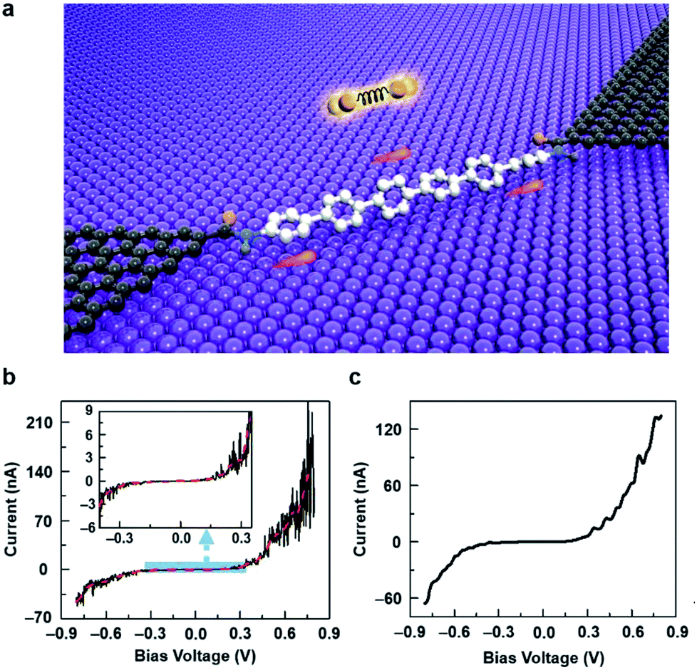 | ||
| Fig. 1 (a) Schematic of a SMJ based on graphene nanoelectrodes. (b) Black line: I–V curve of a representative device measured with a scan step of 1.6 mV. Red line: the fluctuation-suppressed baseline from the black line, highlighting the asymmetric distribution of the I–V curve. Inset: an enlarged view at low bias voltages. (c) I–V curve of the device measured with a scan step of 20 mV. | ||
Results and discussion
Fig. 1b and c show the I–V curves of a representative device measured at scanning steps of 1.6 mV and 20 mV, respectively. In comparison with the conducting performance in the fast scan, the slow scan irritated larger current fluctuations especially at high bias voltages. In addition, we also observed that the current fluctuation was more likely to appear monodirectionally rather than show a symmetric distribution at positive and negative polarities, which has been further verified by subsequent real-time measurements. It should be noted that, in order to explore the asymmetric fluctuation, we also implemented a recurrence average filter (n = 250) computation, an operation that could decrease the high-frequency symmetric noise, which protruded the asymmetric factors in the current distribution. Fig. 2 displays the smoothed I–t profiles of a representative single-molecule device at different bias voltages and the corresponding distribution histograms. We found that at the zero bias, the electric current as a function of time is composed of two parts: the main baseline in the center and minor excursions at negative and positive polarities, both of which gave rise to a Gaussian-histogram distribution. However, the positive bias voltages would generate irregular-shaped, stochastic, and up-direction fluctuations, resulting in an asymmetric distribution tail in the histogram. Furthermore, the asymmetric extent would be aggravated along with the increase of the bias voltage until a transition voltage, beyond which the asymmetric fluctuation began to submerge into the broadened baseline. Current fluctuations at negative bias voltages shared the same characteristics as that at positive bias voltages except for the opposite excursion direction. Similar phenomena were reproducibly observed on other 4 molecular devices tested within the same conditions (see Fig. S4–S7†).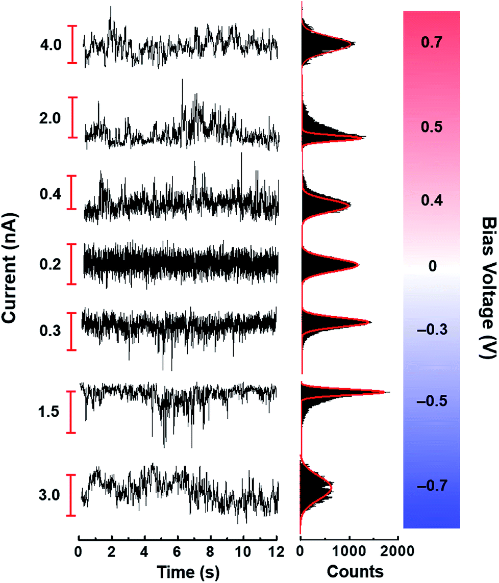 | ||
| Fig. 2 Smoothed I–t profiles of a representative single-molecule device at different bias voltages. The right panel shows the corresponding distribution histograms. The red line is fitted in a Gaussian function according to the steep side of the histogram, highlighting the asymmetric tail. | ||
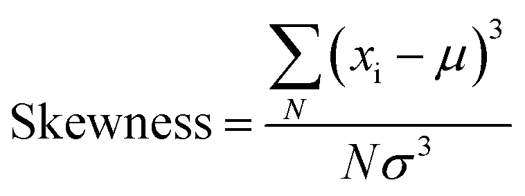
We proposed the normalized third moment, namely the skewness, to describe the asymmetry of the current distribution, which is commonly defined as the expected value of the cubed z-scores in the current distribution:
 | (E1) |
 | ||
| Fig. 3 The relationship between skewness and applied bias voltages. (a) For a representative single-molecule device. Triangular symbols point out the extrema of the skewness. (b) For a graphene nanoconstriction. (c) For a carbon film resistor. | ||
We found that temperature was an important factor affecting the asymmetric intensity of the current distribution. For example, at the applied bias of 0.3 V, the asymmetric current distribution was gradually suppressed following the decrease of the temperature from 295 K to 80 K (Fig. 4), indicating a positive correlation between the temperature and the observed skewness (Fig. 5a). It should be noted that the effect of temperature would be significant when the bias voltage exceeds the threshold for phonon emission.37 Therefore, such a strong temperature correlation in our investigation implies that the phonon-assisted processes could occur in the electronic transport.
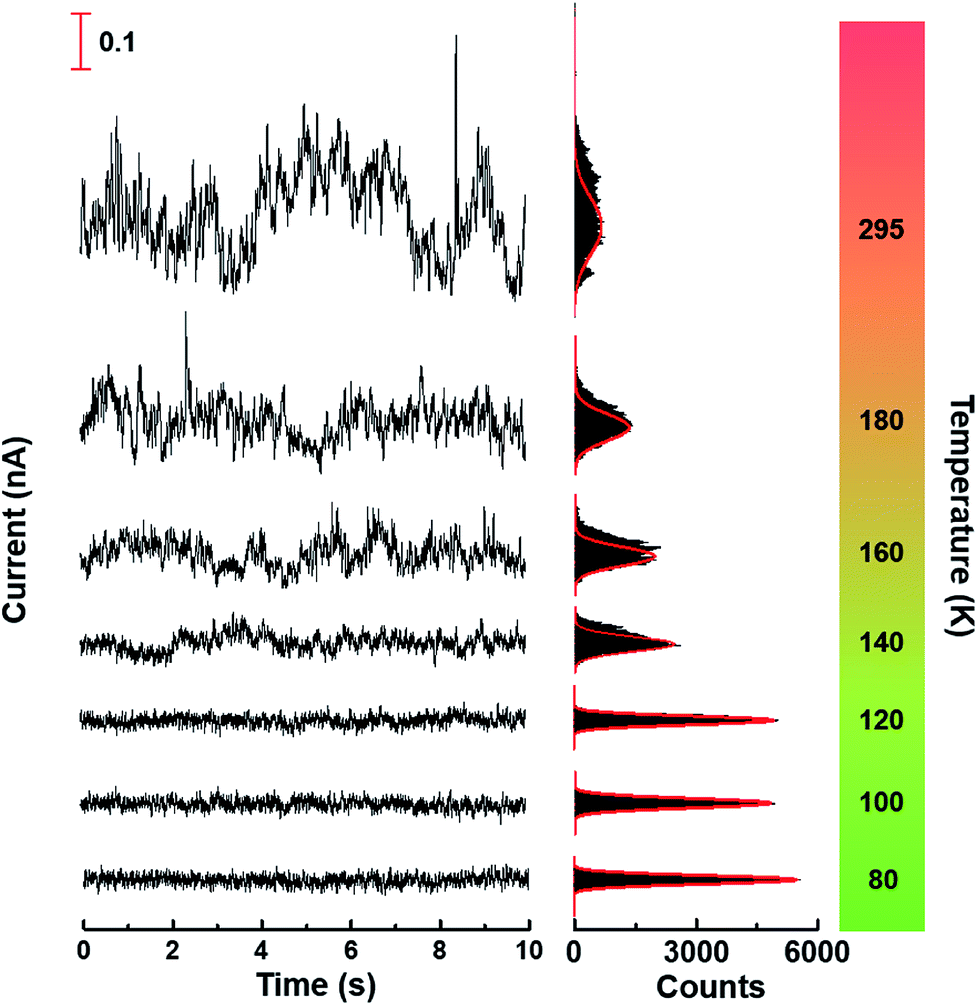 | ||
| Fig. 4 Temperature dependence of I–t profiles of a representative single-molecule device measured at 0.3 V. The red line is fitted in Gaussian function according to the steep side of the histogram, aiming to emphasize the asymmetric tail. | ||
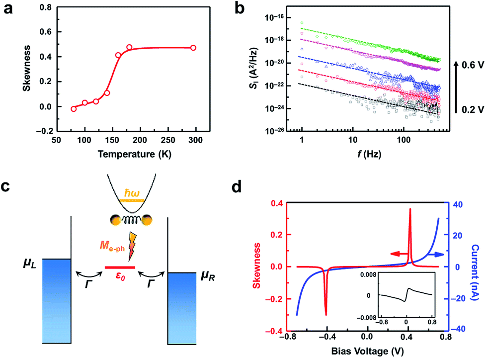 | ||
| Fig. 5 (a) The relationship between the skewness of the current distribution and the temperature derived from Fig. 4. (b) The noise power spectrum at representative voltages in Fig. 2. (c) Schematic of the electron–phonon coupling model in SMJs. (d) Theoretically simulated curves of the dependence of the skewness (red) and the electric current (blue) on the applied biases. Inset: skewness–bias voltage dependence when inelastic corrections are not considered. | ||
Fig. 5b shows the noise power spectra of SMJs at different bias voltages (from 0.2 V to 0.6 V), in which all the spectra follow a classical 1/f power decay law. However, we found that the skewness still exist even when the 1/f noise was totally reduced from the I–t profiles, illustrating that the skewed current distribution was controlled by some unknown high-frequency mechanism rather than 1/f noise. One may wonder what information higher-order moments may carry about the interactions within the junction. To solve this question, model Hamiltonian calculations were carried out based on a simple single-level model using the non-equilibrium Green's function (NEGF) formalism. In our model, the transport behaviour is assumed to be determined by a single molecular level that is positioned at ε0 and symmetrically couples to the two electrodes with the strength Γ; inelastic corrections involve a molecular vibration mode with an energy ħω and the electron–vibration coupling matrix Me–ph, and its populations is given by the Bose–Einstein distribution (Fig. 5c). No other approximations like the extended wideband limit were used in order to investigate the general case of a device at room temperature. By using standard manipulation of the generalized Keldysh Green's function formulism of full counting statistics (FCS),38,39 we could calculate any nth-order cumulant of the current distribution. Within this framework, the third-order cumulant ≪δI3≫ is expressed as the third derivative of the so-called moment generating function S(λ) with respect to λ, where λ is the time-dependent counting field containing any complexity,
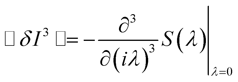 | (E2) |
We set up the model parameters evaluated from the experimental measurements: we assumed a symmetric weak coupling (ΓL = ΓR = 4.2 meV) between the electronic energy level and the two leads, and the electronic energy level position ε0 was set to −0.42 eV, the vibration energy ħω was 50 meV and the electron-vibration coupling matrix Me–ph was 1.5 meV. The temperature was 300 K. The plot of the skewness–bias relation presented two peaks centered at 0.4 V and −0.4 V, showing a trend similar to the experimental measurements. This result is rather robust: peaks always appeared in the skewness–bias curve when the level position ε0, the electronic couplings ΓL and ΓR, the vibration energy ħω and the electron–vibration coupling matrix Me–ph were varied in a wide range (see Fig. S12 and S13†). Admittedly, the peak positions and intensities depend critically on the specific values of these parameters. When compared with the measured results, these two peaks are much narrower. This might be improved when taking into account more different molecular vibration modes and the non-equilibrium local ionic heating effects. It should be mentioned that the peak voltage in the skewness–voltage curve does not correspond to the energy of phonon although the units of both parameters seem similar to some extent. In fact, the peak voltage is determined by various parameters as discussed above.
In contrast, without this inelastic correction the calculated electric current only shows much weaker skew peaks at around ± 0.1 V (the inset in Fig. 5d). Therefore, our simulations demonstrate that the electron–vibration coupling is responsible for the appearance of maxima in the skewness of the current distribution as a function of the applied bias. This theory also explains the origin of multi-peaks observed in the skewness–voltage relationship (Fig. 3a, S11c and S11f†). We think that the multi-peak voltages may be primarily related to different vibration modes of the molecules.
Although graphene nanoconstrictions and molecular junctions showed qualitatively similar I–V characteristics and noise behaviours (Fig. S10†), the skewness of the current distribution was totally different. The asymmetric fluctuation is more obscure in graphene nanoconstriction. We attributed this phenomenon to the low possibility of electron–phonon coupling. For the homojunctions like graphene nanoconstrictions, the vibration modes in the electrodes and the channel are rather similar, which means that electron-induced phonons in the conductive channel are easily dissipated due to the low scattering possibility at the interfaces between the channel and the electrodes.40 On the contrary, the vibration modes of the electrodes and the molecule mismatch each other in graphene–molecule–graphene heterojunctions, which generates significant interface scattering. As a result, SMJs are more easily to be affected by electron-induced phonons via an inelastic electron tunneling process. It is worthwhile to mention again that the theoretical results demonstrated that the skewness of the current distribution obviously decreased and reached an extremum at the vicinity of ±0.1 V when the inelastic corrections are not considered in the calculation model (the inset in Fig. 5d). It also shows similarity to the experimental results in graphene nanoconstrictions (Fig. 3b), providing an evidence that few inelastic processes in the homojunctions lead to less asymmetric fluctuations.
Conclusions
In conclusion, we presented an exploration toward higher-order moments in the current distribution analysis of graphene–molecule–graphene SMJs, which could accommodate covalent electrode–molecule interfaces and the feasibility of real-time signal monitoring in a long time. The skewness or third-order moment was applied to describe the asymmetric current fluctuation and its relationship with the bias voltage and temperature. Theoretical calculations proved that the asymmetry current distribution mainly originated from the inelastic electron tunneling process. In comparison with the ordinary noise analysis based on the noise power, the third-order moment analysis is particularly attractive because it provides more information about the electrical properties of SMJs, for example the electron-vibration coupling that is hard to be accessed at room temperature, thus showing great promise to improve better understanding of the charge transport mechanism in different types of single-molecule devices.Experimental
1. Device fabrication
The single-molecule devices were fabricated on the basis of a “dash-line lithographic” method described in detail elsewhere.41 Cu foils were immersed into acetic acid for 20 minutes in advance, in order to reduce the oxide layer on the surface. After immersion, Cu foils were flushed by abundant ultrapure water and dried by air. Cu foils were loaded on the quartz substrate in the tube furnace, and then annealed at 1045 °C under H2 flow at 75 Pa (12 cm3 min−1) for 1 hour. After annealing, 1.1 cm3 min−1 of CH4 was introduced to the system for 20 minutes. Then the furnace was cool down to room temperature. A poly-methyl methacrylate (PMMA) layer was spin-coated on graphene-covered Cu foils, and then the Cu foil was etched by a ferric trichloride solution. The PMMA-graphene layers were transferred to a 300 nm SiO2/Si wafer. After drying, PMMA was dissolved by the boiling acetone. With the protection of a photolithographically patterned resist mask, graphene was fabricated into a 40 μm graphene sheet by a selective oxygen reactive plasma etching (RIE) process. Metallic electrodes (8 nm Cr + 60 nm Au) were thermally evaporated on the graphene to obtain graphene transistors (see Fig. S1a and S1f†). A dash-line lithographic method was carried on with an electron beam lithography. A 5 nm-width dash line (140 nm segments and 50 nm spaces) was exposed on the specific position of the PMMA mask. After development, selective oxygen RIE was applied to etch the graphene exposed from the dash-line window. By careful control of etching, graphene point contact arrays were obtained, forming an open circuit. After the PMMA resist was rinsed by acetone, the device was soaked into a pyridine solution containing amide terminated hexphenyl molecular chain and a carbodiimide dehydrating agent 1-ethyl-3-(3-dimethylaminopropyl) carbodiimide hydrochloride (EDCI). The detailed synthesis process is provided in the ESI† (Section 1). After 72 hours, the device was taken out from the solution, rinsed with abundant ultrapure isopropanol and acetone, and dried by gentle nitrogen stream (Fig. S1b–S1e and S1g–S1j†). Statistics illustrated that most devices are single-molecule devices (see ESI Section 2 †).2. Device characterization
An Agilent 4155C semiconductor characterization system was used to measure the current–voltage (I–V) characteristics of single-molecule devices. The scan range was set from −0.8 V to 0.8 V. Current–time (I–t) trajectories could be obtained by DL 1211 Current Magnifier and Zurich Instrument HF2LI Lock-in Amplifier. The detailed measurement apparatus was shown in Fig. S2.† The applied voltage (VD) was set as a constant within each trajectory and VD was set from −0.8 V to 0.8 V with a step of 50 mV in different trajectories. For all real-time experiments, the I–t measurement was collected at the rate of 14.4 kHz and last for at least 20 seconds.Conflicts of interest
The authors declare no conflicts of interest.Acknowledgements
We acknowledge primary financial supports from National Key R&D Program of China (2017YFA0204901), the National Natural Science Foundation of China (grants 21727806, 61671021 and 61621061), the Natural Science Foundation of Beijing (Z181100004418003), and the interdisciplinary medicine Seed Fund of Peking University.Notes and references
- A. Aviram and M. A. Ratner, Chem. Phys. Lett., 1974, 29, 277 CrossRef CAS.
- J. E. Green, J. W. Choi, A. Boukai, Y. Bunimovich, E. Johnston-Halperin, E. DeIonno, Y. Luo, B. A. Sheriff, K. Xu, Y. S. Shin, H. R. Tseng, J. F. Stoddart and J. R. Heath, Nature, 2007, 445, 414 CrossRef CAS PubMed.
- M. Elbing, R. Ochs, M. Koentopp, M. Fischer, C. von Hanisch, F. Weigend, F. Evers, H. B. Weber and M. Mayor, Proc. Natl. Acad. Sci. U. S. A., 2005, 102, 8815 CrossRef CAS PubMed.
- I. Diez-Perez, J. Hihath, Y. Lee, L. P. Yu, L. Adamska, M. A. Kozhushner, I. I. Oleynik and N. Tao, Nat. Chem., 2009, 1, 635 CrossRef CAS PubMed.
- S. Sherif, G. Rubio-Bollinger, E. Pinilla-Cienfuegos, E. Coronado, J. C. Cuevas and N. Agrait, Nanotechnology, 2015, 26, 291001 CrossRef PubMed.
- B. Capozzi, J. L. Xia, O. Adak, E. J. Dell, Z. F. Liu, J. C. Taylor, J. B. Neaton, L. M. Campos and L. Venkataraman, Nat. Nanotechnol., 2015, 10, 522 CrossRef CAS PubMed.
- B. Y. Choi, S. J. Kahng, S. Kim, H. Kim, H. W. Kim, Y. J. Song, J. Ihm and Y. Kuk, Phys. Rev. Lett., 2006, 96, 156106 CrossRef PubMed.
- S. J. van der Molen and P. Liljeroth, J. Phys.: Condens. Matter, 2010, 22, 133001 CrossRef PubMed.
- C. Jia, A. Migliore, N. Xin, S. Huang, J. Wang, Q. Yang, S. P. Wang, H. Chen, D. Wang, B. Feng, Z. Liu, G. Zhang, D. Qu, H. Tian, M. A. Ratner, H. Xu, A. Nitzan and X. Guo, Science, 2016, 352, 1443 CrossRef CAS PubMed.
- N. Xin, J. Wang, C. Jia, Z. Liu, X. Zhang, C. Yu, M. Li, S. Wang, Y. Gong, H. Sun, G. Zhang, Z. Liu, G. Zhang, J. Liao, D. Zhang and X. Guo, Nano Lett., 2017, 17, 856 CrossRef CAS PubMed.
- H. Song, Y. Kim, Y. H. Jang, H. Jeong, M. A. Reed and T. Lee, Nature, 2009, 462, 1039 CrossRef CAS PubMed.
- R. P. Andres, T. Bein, M. Dorogi, S. Feng, J. I. Henderson, C. P. Kubiak, W. Mahoney, R. G. Osifchin and R. Reifenberger, Science, 1996, 272, 1323 CrossRef CAS PubMed.
- W. Wang, Y. Ji, H. Zhang, A. Zhao, B. Wang, J. Yang and J. G. Hou, ACS Nano, 2012, 6, 7066 CrossRef CAS PubMed.
- L. Chen, Z. Hu, A. Zhao, B. Wang, Y. Luo, J. Yang and J. G. Hou, Phys. Rev. Lett., 2007, 99, 146803 CrossRef PubMed.
- V. Madhavan, W. Chen, T. Jamneala, M. F. Crommie and N. S. Wingreen, Science, 1998, 280, 567 CrossRef CAS PubMed.
- Z. J. Donhauser, B. A. Mantooth, K. F. Kelly, L. A. Bumm, J. D. Monnell, J. J. Stapleton, D. W. Price, A. M. Rawlett, D. L. Allara, J. M. Tour and P. S. Weiss, Science, 2001, 292, 2303 CrossRef CAS PubMed.
- R. A. Wassel, R. R. Fuierer, N. J. Kim and C. B. Gorman, Nano Lett., 2003, 3, 1617 CrossRef CAS.
- T. A. Su, H. Li, M. L. Steigerwald, L. Venkataraman and C. Nuckolls, Nat. Chem., 2015, 7, 215 CrossRef CAS PubMed.
- S. Y. Quek, M. Kamenetska, M. L. Steigerwald, H. J. Choi, S. G. Louie, M. S. Hybertsen, J. B. Neaton and L. Venkataraman, Nat. Nanotechnol., 2009, 4, 230 CrossRef CAS PubMed.
- O. Adak, E. Rosenthal, J. Meisner, E. F. Andrade, A. N. Pasupathy, C. Nuckolls, M. S. Hybertsen and L. Venkataraman, Nano Lett., 2015, 15, 4143 CrossRef CAS PubMed.
- M. Galperin, A. Nitzan and M. A. Ratner, Phys. Rev. B, 2006, 74, 075326 CrossRef.
- S. Kim, Phys. Rev. B, 2014, 89, 035413 CrossRef.
- M. Tsutsui, M. Taniguchi and T. Kawai, Nat. Commun., 2010, 1, 138 CrossRef PubMed.
- N. Neel, J. Kroeger and R. Berndt, Nano Lett., 2011, 11, 3593 CrossRef CAS PubMed.
- H. X. He, J. S. Zhu, N. J. Tao, L. A. Nagahara, I. Amlani and R. Tsui, J. Am. Chem. Soc., 2001, 123, 7730 CrossRef CAS PubMed.
- E. Lortscher, J. W. Ciszek, J. Tour and H. Riel, Small, 2006, 2, 973 CrossRef CAS PubMed.
- R. Arielly, M. Vadai, D. Kardash, G. Noy and Y. Selzer, J. Am. Chem. Soc., 2014, 136, 2674 CrossRef CAS PubMed.
- F. Schwarz, G. Kastlunger, F. Lissel, C. Egler-Lucas, S. N. Semenov, K. Venkatesan, H. Berke, R. Stadler and E. Lörtscher, Nat. Nanotechnol., 2016, 11, 170 CrossRef CAS PubMed.
- D. Cho, S. Shekhar, H. Lee and S. Hong, Nano Lett., 2018, 18, 1001 CrossRef CAS PubMed.
- D. Djukic and J. M. van Ruitenbeek, Nano Lett., 2006, 6, 789 CrossRef CAS PubMed.
- P. J. Wheeler, J. N. Russom, K. Evans, N. S. King and D. Natelson, Nano Lett., 2010, 10, 1287 CrossRef CAS PubMed.
- S. Dallakyan and S. Mazumdar, Appl. Phys. Lett., 2003, 82, 2488 CrossRef CAS.
- G. C. Solomon, A. Gagliardi, A. Pecchia, T. Frauenheim, A. Di Carlo, J. R. Reimers and N. S. Hush, Nano Lett., 2006, 6, 2431 CrossRef CAS PubMed.
- M. A. Reed, C. Zhou, C. J. Muller, T. P. Burgin and J. M. Tour, Science, 1997, 278, 252 CrossRef CAS.
- B. Xu and N. Tao, Science, 2003, 301, 1221 CrossRef CAS PubMed.
- L. Venkataraman, J. E. Klare, C. Nuckolls, M. S. Hybertsen and M. L. Steigerwald, Nature, 2006, 442, 904 CrossRef CAS PubMed.
- R. Avriller and T. Frederiksen, Phys. Rev. B, 2012, 86, 155411 CrossRef.
- F. Haupt, T. Novotny and W. Belzig, Phys. Rev. Lett., 2009, 103, 136601 CrossRef PubMed.
- F. Haupt, T. Novotny and W. Belzig, Phys. Rev. B, 2010, 82, 165411 CrossRef.
- J. T. Lu and J. S. Wang, Phys. Rev. B, 2007, 76, 165418 CrossRef.
- Y. Cao, S. Dong, S. Liu, L. He, L. Gan, X. Yu, M. L. Steigerwald, X. Wu, Z. Liu and X. Guo, Angew. Chem., Int. Ed., 2012, 51, 12228 CrossRef CAS PubMed.
Footnotes |
| † Electronic supplementary information (ESI) available: Molecular synthesis, detailed device characterization and statistics, current–time profile of more single-molecule and control devices, detailed theoretical calculations. See DOI: 10.1039/c8ra08508k |
| ‡ These authors contributed equally to this work. |
| This journal is © The Royal Society of Chemistry 2018 |