
 Open Access Article
 This Open Access Article is licensed under a Creative Commons Attribution-Non Commercial 3.0 Unported Licence
Tunable large-scale regular array of topological defects in nematic liquid crystals†
MinSu Kim and
Francesca Serra*
and
Francesca Serra*
Department of Physics and Astronomy, Johns Hopkins University, Baltimore 21218, USA. E-mail: francesca.serra@jhu.edu
First published on 17th October 2018
Abstract
Arrays of topological defects in liquid crystals are fascinating systems, as isotropic and anisotropic phases of the same material can co-exist and be arranged in regular periodic structures. The arrays thus form spatially-varying optical pathways, in patterns that can be used for optics, as novel photonic structures, optical gratings, lenses or metamaterials, and for molecular and colloidal self-assembly. However, for practical applications, it is necessary that the arrays are tunable without direct intervention of the experimenters. Here, we demonstrate single-domain, tunable arrays of topological defects in nematic liquid crystals, using a method inspired by the recent work by Orihara and colleagues. The regularity and domain size of the defect arrays are obtained by using periodic lateral modulation of electric fields generated by incompletely etched electrodes with periodic conductivity. The period of the arrays, i.e. the characteristic spacing between defects, is controllable not only through the applied electric field strength and frequency but also by varying the size of the patterned electrodes. We believe these results open a new way to design and fabricate large-scale, single-domain, tunable and scalable device architectures that are optically functional.
Introduction
Spontaneous formation of periodic or regular patterns is ubiquitous in nature. Self and directed assembly are powerful tools to mimic nature and create patterns using soft materials, such as block-copolymers,1,2 colloids3,4 and liquid crystals (LCs).5 Among these systems, LCs are useful as they form topological defects, special regions where the LC orientational order is not defined. One can generate defects by surface treatments,6,7 geometric confinements,8,9 or various external stimuli, such as electric field or flow.10 Defect arrays can be used for optics, as arrays of optical vortices,11,12 gratings,13 micro-lens arrays,14 or for other purposes such as templating super hydrophobic surfaces6 or programming the 3D shape of LC elastomers.15–17 However, realizing a regular, periodic array of defects is a nontrivial task and it often requires local manipulation by the experimenter, e.g. with optical or magnetic tweezers and complicated surface treatment,18 combined with heat convection19 or electric fields.20–22One strategy is to exploit the Helfrich-like instability, caused by the electro-hydrodynamic effects in nematic LCs.23–25 The conductivity properties of the LC, combined with the dielectric properties and the initial alignment determine what pattern will be formed when the instability occurs. The instability can generate arbitrarily large two-dimensional patterns where an electric field is applied, but this pattern is generally irregular. This is due in part to the imperfect cleanliness of the surfaces of the LC cell and in part to the presence of ions, which are necessary for the formation of the pattern but whose behavior is difficult to control.
Recently, Orihara's group reported creating two-dimensional grid-like patterns in which umbilical defects with topological charges ±1 are formed near the top and bottom substrates.21 The system consists of LCs with negative dielectric anisotropy with added ions, aligned homeotropically by using an amorphous fluoropolymer with high-resistivity. When AC field is applied under certain conditions a square array of umbilical defects appears (ESI Fig. S1a and b†). In general, this array is highly irregular. The authors outline two strategies to make the pattern uniform:21 (1) electrodes are patterned into thin stripes, then overlapped perpendicularly. The voltage is applied only in square areas, that we will call “field-active”, where the array is formed; (2) irregular areas are locally melted with optical tweezers until they relax to the regular structure. Because the second approach requires direct intervention of experimenters, it cannot be used for tunable systems where the external electric field should be the only control parameter. The first approach is more desirable as it does not require a direct intervention; however, here we show that as the size of electrode becomes large compared to the characteristic spacing between neighboring defects the regularity of the defect array becomes increasingly unstable. We overcome the intrinsic limitation of the previous method by fabricating continuous electrodes with periodic conductivity. We achieve this by etching stripes out of a conductive layer but not completely, in such a way that electrodes are present everywhere but their conductivity is modulated. We can thus apply the vertical electric field everywhere while generating spatially periodic modulation. Thanks to this simple but robust method, the regular array can be extended to arbitrarily large scale. In addition, we show how the presence of patterned electrodes influences the characteristic distance between defects and how this distance can be tuned.
Experimental
Materials and methods
![[thin space (1/6-em)]](https://www.rsc.org/images/entities/char_2009.gif) :HNO3:H2O = 1:0.1:1) until the exposed ITO area was fully etched. For incompletely etched electrodes, we controlled the etching time and monitored the resistivity of the exposed ITO area until the resistivity became 3 orders of magnitude higher than the photoresist covered area. The photoresist residue was removed by acetone thereafter. The homeotropic alignment layer was coated on the patterned electrodes. The substrates were spin-coated (3000 rpm for 30 s) with an amorphous fluoropolymer solution, prepared by mixing a solute (CTL-809M, Asahi Glass Co.), which contains 9 wt% of CYTOP, into a solution (CT-Solv.180, Asahi Glass Co.) with the ratio 1:2 in weight, and then baked (step 1: 70 °C for 30 min; step 2: 120 °C for 30 min) following the protocol in ref. 21. The substrates were assembled while maintaining the cell gap by spacer beads. The empty cell gap was measured by the interferometric method using a UV-VIS spectrometer (Flame, Ocean Optics).cos(2πft), generated by a waveform generator (DS345, SRS, Inc.) and amplified by a power amplifier (Model 2205, Trek, Inc.). We measured voltage-dependent optical transmittance curves (V–T curves) as well as the threshold voltage Vth while fixing f and sweeping V. After measuring the V–T curves and determining the Vth, we were able to apply V and f in such a way that all the images had similar brightness. Between each measurement where both V and f were changed, such as those shown in the sequential images (ESI Videos S1–S7†), the voltage was always dropped below the threshold voltage. V and f were then re-adjusted to the new values and the system observed.
:HNO3:H2O = 1:0.1:1) until the exposed ITO area was fully etched. For incompletely etched electrodes, we controlled the etching time and monitored the resistivity of the exposed ITO area until the resistivity became 3 orders of magnitude higher than the photoresist covered area. The photoresist residue was removed by acetone thereafter. The homeotropic alignment layer was coated on the patterned electrodes. The substrates were spin-coated (3000 rpm for 30 s) with an amorphous fluoropolymer solution, prepared by mixing a solute (CTL-809M, Asahi Glass Co.), which contains 9 wt% of CYTOP, into a solution (CT-Solv.180, Asahi Glass Co.) with the ratio 1:2 in weight, and then baked (step 1: 70 °C for 30 min; step 2: 120 °C for 30 min) following the protocol in ref. 21. The substrates were assembled while maintaining the cell gap by spacer beads. The empty cell gap was measured by the interferometric method using a UV-VIS spectrometer (Flame, Ocean Optics).cos(2πft), generated by a waveform generator (DS345, SRS, Inc.) and amplified by a power amplifier (Model 2205, Trek, Inc.). We measured voltage-dependent optical transmittance curves (V–T curves) as well as the threshold voltage Vth while fixing f and sweeping V. After measuring the V–T curves and determining the Vth, we were able to apply V and f in such a way that all the images had similar brightness. Between each measurement where both V and f were changed, such as those shown in the sequential images (ESI Videos S1–S7†), the voltage was always dropped below the threshold voltage. V and f were then re-adjusted to the new values and the system observed.Results and discussion
We verify the dependency of the characteristic spacing between defects l on the frequency f and the voltage V in our sample (see ESI Fig. S1c–e and Video S1† for sequential images) using a mixture of CCN-47 and CCN-55. The spacing l is proportional to V and inversely proportional to f1/2 (ESI Fig. S1d and e†) in the range between lmin ∼ 9.5 and lmax ∼ 15 μm where the thickness is d ∼ 3.7 μm. The range of allowed spacing strongly depends on d, as reported.21 However, the arrangement of the defects is irregular, and the single domain order is short range.We fabricate cells with ITO electrodes patterned in thin stripes and arranged perpendicularly. Strong lateral electric fields form along both polar and azimuthal angles at the electrode edges (Fig. 1a–c). We vary the electrode width from w = 100 to 40 μm (Fig. 1e–i) and define parameters as the length of the area lA containing the regular defect array and the distance between neighboring defects lw (Fig. 1d). It is immediately evident that lA does not span the whole width w, and that the defect array encompasses a fraction of the total area. In the most general case, without appropriate tuning of V and f, the array is still irregular. However, by spanning a wide range of V and f it is possible to find combinations of parameters that produce regular arrays, where lw = lA/(N − 1). The measured number of umbilical defects Nm in each row of the array is an odd number whenever arrays are regular. Nm can be visualized in the images as the number of dark vertical lines (Fig. 1d). Nm can be tuned by changing V and f. In transient states between consecutive odd values of Nm, we can observe either dislocations in the defect arrays or randomly disoriented arrays (see ESI Videos S2–S6† for sequential images).
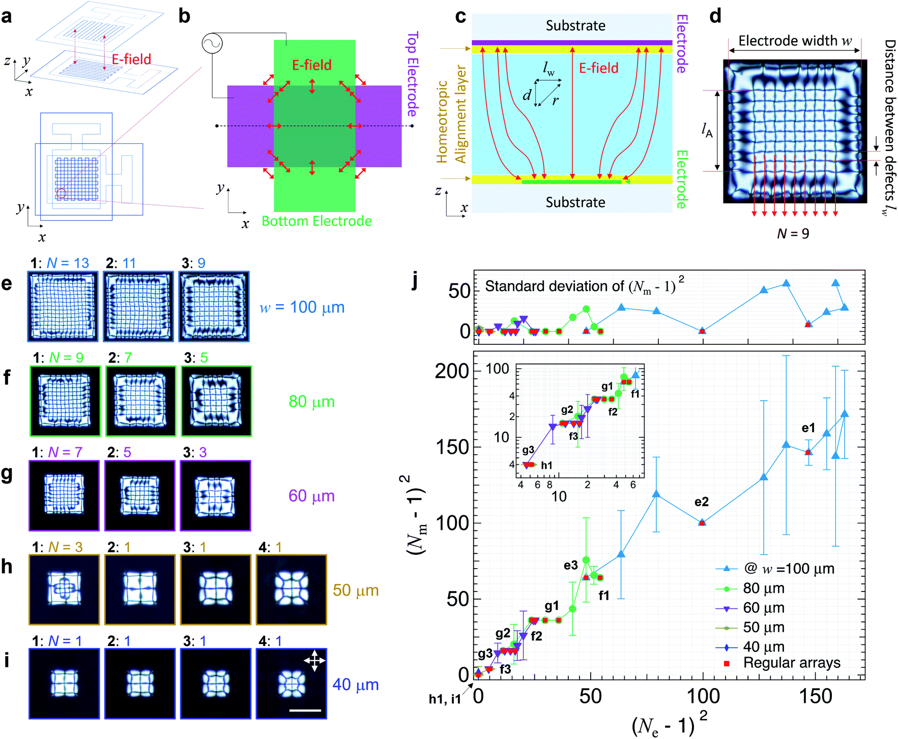 | ||
Fig. 1 The electrode-confinement effect and regular arrays. (a) Schematics of the LC cell. (b and c) Schematics of the applied field lines (red arrows) (b) in the x–y and (c) x–z planes (the scales in x- and z-axes are different). (d) Measurable parameters of the array. (e–i) Polarizing optical microscopy (POM) images of defect arrays with different w (see also ESI Videos S2–S6† for sequential images). The scale bar is 50 μm. (j) Measured (Nm − 1)2 with respect to estimated  . Upper: the standard deviation of (Nm − 1)2; inset: logarithmic scale where (Nm − 1)2 < 100. . Upper: the standard deviation of (Nm − 1)2; inset: logarithmic scale where (Nm − 1)2 < 100. | ||
To understand the behavior of the LCs, we first consider the response of both LCs and ions in the system, as outlined in ref. 23–25. The ion and director relaxation times can be determined as τion = ε0εr/σ and τLC = γd2/(Kπ2 − εV2), respectively, where γ is the LC viscosity. We assume the splay (K11), twist (K22) and bend (K33) elastic constants to be all equal to K; ε = ε0εr; ε0, εr and σ are the vacuum permittivity, the relative permittivity (dielectric constant) and conductivity, respectively.25 The ion relaxation time is shorter than inverse of field-frequency, that is, τion < τLC ∼ (2f)−1. We consider the director relaxation in the z-axis and x–y plane by the vertical and the lateral components of electric fields, respectively, and introduce the total displacement r2 = d2 + lw2 (inset in Fig. 1c). Thus, 2f = (Kπ2 − εV2)/γ(r2 − lw2). In the absence of patterned electrodes and lateral confinement, lw depends on d, V and f. In our system, we can show that it is affected by w and more specifically by lA. We measure lw, lA and N independently. By replacing lw = lA/(N − 1), we are able to describe the estimated total number of “squares”, i.e., areas between umbilical defects in a regular arrangement, as 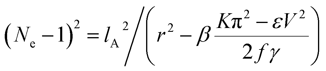 , where Ne is the estimated number of defects per line. Here, due to the difficulty in determining a single value for the viscosity γ in this composite system, we leave β as a free parameter. In this way, β can account also for the imprecisions associated with K and ε. We set the material properties as K = 10−11 [N], |Δε| = 5, ε0 = 8.85 × 10⁻¹² [N V−2], γ = 0.1 [Pa s].27 In Fig. 1j, we plot (Nm − 1)2, the measured value, as a function of the estimated value (Ne − 1)2.
Three observations emerge from the plot in Fig. 1j. First, measurements and theory are in a good agreement, confirmed by the fact that the fitting parameter β is fairly close to 1. Second, it is evident that if the set of parameters is close enough to those of a regular array, there is a high energy cost associated with disrupting the array. This is particularly evident in the case of the smaller electrodes. Third, the standard deviation, measured by counting the number of defects over many repetitions of the experiments, increases as the electrode size increases. In other words, as the electrodes get bigger it is harder to get the right set of parameters that will guarantee the regularity of the array.
It is evident that the latter consideration hinders the possibility of using very large electrodes to create arbitrarily large-scale arrays. However, large electrodes would be desirable because that would reduce the effects of edges, where the array is not regular, as shown in ESI Fig. S1d–i and S2.† For large-scale arrays, these edges should be removed. Similarly, we need to find a way to eliminate the “dead” areas, where there are no electrodes.
To overcome this impasse, we etch the electrodes only partially. In this way, the electric field is applied over the entire area while still maintaining a non-zero x–y component at the boundary between non-etched and incompletely-etched parts (Fig. 2a). The defect array can be thus continuously arranged over a large area (Fig. 2b–d). A PolScope microscopy image can confirm the LC director profile in the x–y plane (Fig. 2b). In Fig. 2, one can still clearly see some dislocations highlighted in the red-dotted rectangles (Fig. 2c). The study of the dynamics of such dislocations is of interest to us, but outside the scope of this paper. Here, instead, we focus on how to eliminate these “defects in defects” in order to make regular arrays.
 | ||
| Fig. 2 Incomplete etching for large-scale arrays. (a) The red arrows represent electric field formation in the x–z plane. (b) A PolScope microscopy image of a defect array. The dark lines and the color map represent LC directors. The scale bar is 20 μm. (c and d) POM images (c) without or (d) with a full-wave plate. The array is obtained with w = 100 μm, V = 15 V, f = 500 Hz. The inset is the 2D-FFT of the array in (c). The yellow arrow represents the full-wave-plate. Defects in defect arrays are highlighted in the red-dotted rectangle. The slightly shaded stripes in (c) and (d) correspond to the non-etched parts of the electrodes, while the clearer parts are incompletely etched. The scale bar is 100 μm. | ||
To enhance the regularity, we use fine electrode patterning. A specially designed photomask allows us to observe the effect of electrodes with w = 10, 20, and 30 μm within an area of about a square millimeter (Fig. 3a). We first measure l with plain electrodes, finding that l ranges from lmin ∼ 14 to lmax ∼ 35 μm at d = 7.8 μm (Fig. 3b and c). We then proceed to the system which uses incompletely etched electrodes. We see that for this system the regular arrays occur where lw,m ∼ w, that is, the number of defects n per electrode is 1 (see Fig. S3, ESI†). Here, n is the number of defects per electrode for the incompletely etched electrodes while we use N for the completely etched electrodes. We measure lw,m with w = 20 and 30 μm and plot it as a function of  , an expected value of lw obtained with the same procedure used to estimate Ne (Fig. 3d). Here, the same value determined for Fig. 1j is used for the parameter β. A regular array with lw,m ∼ 20 μm appears in the area covered by electrodes with w = 20 μm (V = 10 V, f = 76 Hz, Fig. 3e), and an array with lw,m ∼ 30 μm appears when w = 30 μm (V = 25 V, f = 28 Hz, Fig. 3f) (see ESI Videos S7† for sequential images). In this case, the effect of lateral confinement from the electrodes is more dramatic. For a fixed set of parameters the different size of electrodes leads to significant variations of lw,m from the expected value lw,e. In particular, the large confinement exerted by the electrode with w = 20 μm is able to keep the lw,m constant at w = 20 μm even when lw,e in a “free” system could be much larger. This finding is promising for the creation of bistable systems.
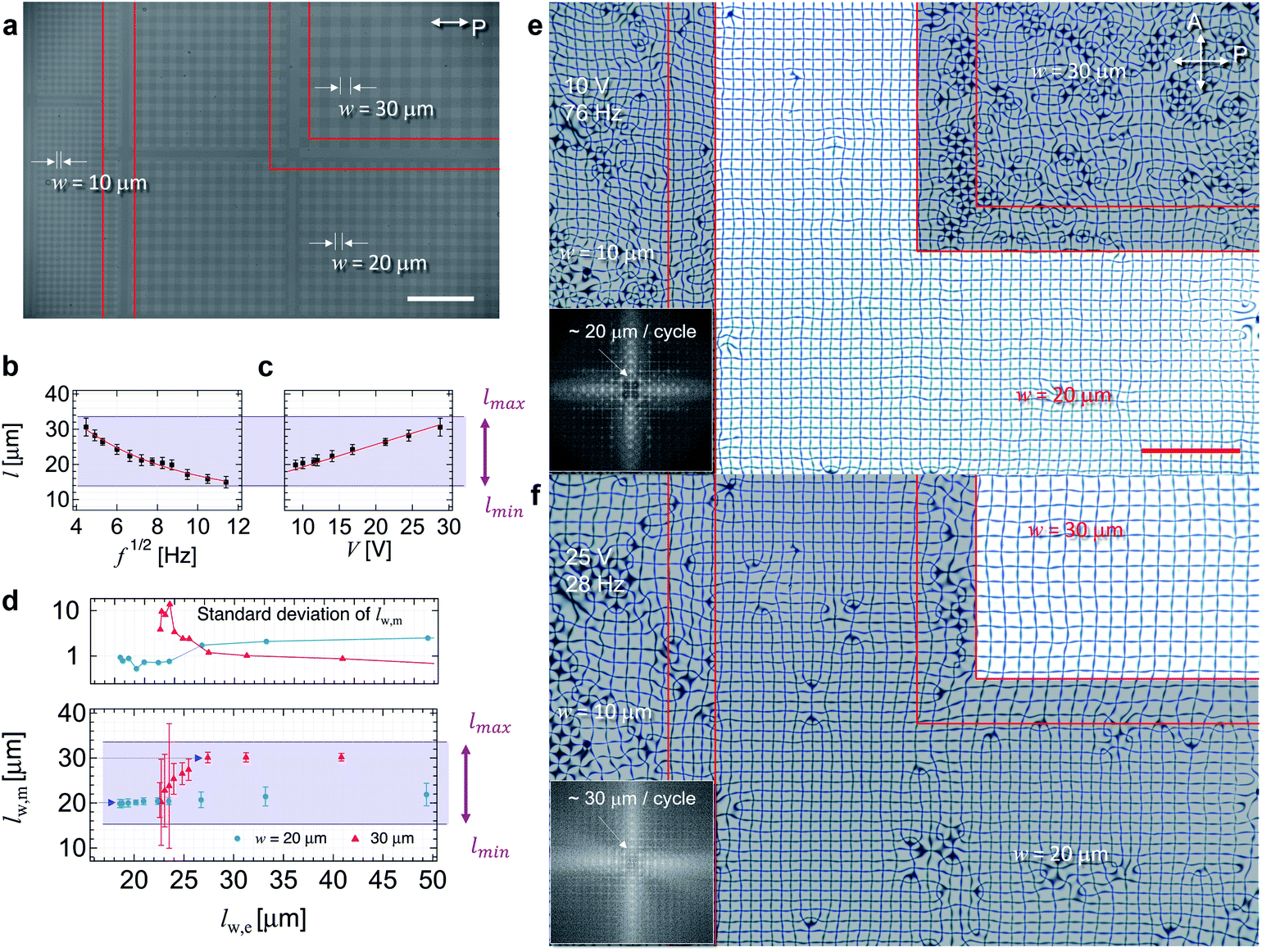 | ||
Fig. 3 Control of large-scale arrays. (a) Electrodes with w = 10, 20 and 30 μm when LC is homeotropically aligned and no voltage is applied. The red lines indicate boundaries. The scale bar is 200 μm. (b and c) Measured l as a function of (b) f and (c) V, at d = 7.8 μm. (d) The measured lw,m and its standard deviation (upper panel) with respect to estimated  . The blue-single-headed arrows indicate that the regular array appears where lw ∼ w. (e and f) POM images under (e) 10 V at 76 Hz and (f) 25 V at 28 Hz (see ESI Videos S7† for sequential images). The brighter areas highlight regular arrays at w = (e) 20 and (f) 30 μm. Each inset is the 2D-FFT of the regular region. The scale bar is 200 μm. . The blue-single-headed arrows indicate that the regular array appears where lw ∼ w. (e and f) POM images under (e) 10 V at 76 Hz and (f) 25 V at 28 Hz (see ESI Videos S7† for sequential images). The brighter areas highlight regular arrays at w = (e) 20 and (f) 30 μm. Each inset is the 2D-FFT of the regular region. The scale bar is 200 μm. | ||
To verify the existence of arrays for wider electrodes, where n > 1, we observe and measure the quantities using electrodes with w = 10, 20, 30, 40 and 50 μm and d ∼ 3.7 μm (Fig. 4). By changing lw,e through V and f, we observe the relation of lw,m with respect to w and n (ESI Table S1†). At w = 10 μm (Fig. 4a), n = 1 and lw,m ∼ 10 μm is constant for the entire explored range of V and f; at w = 20 μm (Fig. 4b), lw,m ∼ 6.7 μm with n = 3 (lw,e ∼ w/n ∼ 20/3 μm); at w = 30 μm (Fig. 4c), lw,m ∼ 10 μm and n = 3; at w = 40 μm (Fig. 4d), lw,m ∼ 7.9 or 13.1 μm with n = 5 or 3; at w = 50 μm (Fig. 4e), lw,m ∼ 7.1 or 10 μm with n = 7 or 5 (see details in ESI Table S1†). The red fonts in Table S1† indicate irregular arrays during the transient states (large images are available in ESI Fig. S4 and S5†). These measurements show an “odd-even” effect. If a regular array can stably form with 10 μm electrodes (Fig. 4a), the same array is not as stable with a 20 μm electrode (Fig. 4b). The reason is intuitive: doubling the number of defects per line does not satisfy the boundary conditions at the electrode edge. One defect with winding number −1 will be next to one corner while a defect with winding number +1 will be next to the other. Only adding a third defect on the line will restore the same LC orientation next to the electrode edge (Fig. 4f). As expected, the network formed with the 20 μm electrode is frustrated and easily disrupted, while the network formed with the 30 μm electrode (Fig. 4c) is regular. The same is valid for the 40 and 50 μm electrodes (Fig. 4d and e). This can be seen clearly in the Fourier spectrum of the array, shown in ESI Fig. S7.† We notice, however, that other effects can come into play for large electrodes such as the 50 μm electrodes. The image in the second column in Fig. 4e shows a “transition” between a finer array spacing in the upper part of the figure with n = 7 and a coarser array in the lower part of the figure with n = 5. This, once again, confirms the importance of using finer electrodes to guarantee the regularity of the array. On the other hand, using wider electrodes can allow for the formation of multi-stable systems with different periodicity. Finally, in this system the only limitations to the size of the array are given by the size of the patterned electrode area (i.e. the area of the photomask) and by the impurities of the surface. We can exactly map the imperfections in our defects arrays onto random impurities on the surface, as shown in ESI Fig. S8.† As these limitations can be easily overcome with cleanroom preparation, these arrays can be extended over areas of many square centimetres, and thus provide a suitable platform for applications.
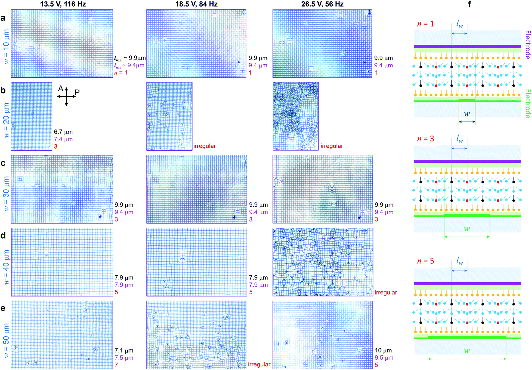 | ||
| Fig. 4 The size dependence of regular arrays with respect to the electrode width w = (a) 10, (b) 20, (c) 30, (d) 40, and (e) 50 μm. The regular array appears when lw = w/n, where n is an odd number. When w/n is out of the range of lw or it is in a transient state between odd numbers, the array becomes irregular. The scale bar is 100 μm (large scale images available in ESI Fig. S4 and S5†). (f) Schematics of director fields with n = 1, 3, and 5. | ||
Conclusions
We investigated how the lateral electric field confinement applied through finely patterned electrodes helps accommodate regular arrays of umbilical defects. We can control the spacing between neighboring defects and show tunable large-scale regular defect arrays solely controllable via electric fields. We study the role of the electrode size in the generation of the regular arrays induced by electric fields using a negative dielectric anisotropy material. The characteristic spacing and the number of defects were defined with respect to the properties of the materials and the other measured physical quantities. We found that the key to have very regular arrays is to use thin electrodes, with sizes comparable to the characteristic distance between the defects. Thanks to the stratagem of incompletely etching the electrodes, we can generate large-scale periodic electric fields that are slightly modulated, thereby producing regular defect arrays with no spatial limitation. In this way, the array is regular and tunable only via electric field, without the need for the direct intervention of the experimenters. This outlines a new route to design large-scale arrays that are self-assembled and tunable, and that can be used as multi-functional devices, optical gratings or as sites for particle assembly.Conflicts of interest
There are no conflicts to declare.Acknowledgements
We thank JHU for funding, Kirsten Endresen for useful feedback, and Nematel GmbH & Co. KG for materials.Notes and references
- G. Krausch and R. Magerle, Adv. Mater., 2002, 14, 1579–1583 CrossRef CAS.
- S. B. Darling, Prog. Polym. Sci., 2007, 32, 1152–1204 CrossRef CAS.
- J. Zhang, Y. Li, X. Zhang and B. Yang, Adv. Mater., 2010, 22, 4249–4269 CrossRef CAS PubMed.
- V. Lotito and T. Zambelli, Adv. Colloid Interface Sci., 2017, 246, 217–274 CrossRef CAS PubMed.
- I. W. Hamley, Angew. Chem., Int. Ed., 2003, 42, 1692–1712 CrossRef CAS PubMed.
- Y. H. Kim, D. K. Yoon, H. S. Jeong, J. H. Kim, E. K. Yoon and H. T. Jung, Adv. Funct. Mater., 2009, 19, 3008–3013 CrossRef CAS.
- M. Wang, Y. Li and H. Yokoyama, Nat. Commun., 2017, 8, 388 CrossRef PubMed.
- F. Serra, K. C. Vishnubhatla, M. Buscaglia, R. Cerbino, R. Osellame, G. Cerullo and T. Bellini, Soft Matter, 2011, 7, 10945 RSC.
- S. Shojaei-Zadeh and S. L. Anna, Langmuir, 2006, 22, 9986–9993 CrossRef CAS PubMed.
- I. Dierking, O. Marshall, J. Wright and N. Bulleid, Phys. Rev. E, 2005, 71, 061709 CrossRef CAS PubMed.
- P. J. Ackerman, Z. Qi and I. I. Smalyukh, Phys. Rev. E: Stat., Nonlinear, Soft Matter Phys., 2012, 86, 021703 CrossRef PubMed.
- R. Barboza, U. Bortolozzo, G. Assanto, E. Vidal-Henriquez, M. G. Clerc and S. Residori, Phys. Rev. Lett., 2013, 111, 093902 CrossRef CAS PubMed.
- P. J. Ackerman, Z. Qi, Y. Lin, C. W. Twombly, M. J. Laviada, Y. Lansac and I. I. Smalyukh, Sci. Rep., 2012, 2, 414 CrossRef PubMed.
- F. Serra, M. A. Gharbi, Y. Luo, I. B. Liu, N. D. Bade, R. D. Kamien, S. Yang and K. J. Stebe, Adv. Opt. Mater., 2015, 3, 1287–1292 CrossRef CAS.
- M. E. McConney, A. Martinez, V. P. Tondiglia, K. M. Lee, D. Langley, I. I. Smalyukh and T. J. White, Adv. Mater., 2013, 25, 5880–5885 CrossRef CAS PubMed.
- T. H. Ware, M. E. McConney, J. J. Wie, V. P. Tondiglia and T. J. White, Science, 2015, 347, 982–984 CrossRef CAS PubMed.
- Y. Xia, G. Cedillo-Servin, R. D. Kamien and S. Yang, Adv. Mater., 2016, 28, 9637–9643 CrossRef CAS PubMed.
- B. S. Murray, R. A. Pelcovits and C. Rosenblatt, Phys. Rev. E: Stat., Nonlinear, Soft Matter Phys., 2014, 90, 052501 CrossRef PubMed.
- P. Pieranski, E. Dubois-Violette and E. Guyon, Phys. Rev. Lett., 1973, 30, 736–739 CrossRef CAS.
- C. Peng, Y. Guo, C. Conklin, J. Viñals, S. V. Shiyanovskii, Q. H. Wei and O. D. Lavrentovich, Phys. Rev. E: Stat., Nonlinear, Soft Matter Phys., 2015, 92, 052502 CrossRef PubMed.
- Y. Sasaki, V. S. R. Jampani, C. Tanaka, N. Sakurai, S. Sakane, K. V. Le, F. Araoka and H. Orihara, Nat. Commun., 2016, 7, 13238 CrossRef CAS PubMed.
- L. K. Migara and J.-K. Song, NPG Asia Mater., 2018, 10, e459 CrossRef.
- W. Helfrich, J. Chem. Phys., 1969, 51, 4092–4105 CrossRef CAS.
- E. Dubois-Violette, P. G. d. Gennes and O. Parodi, J. Phys., 1971, 32, 305–317 CrossRef CAS.
- A. Hertrich, W. Decker, W. Pesch and L. Kramer, J. Phys. II, 1992, 2, 1915–1930 CrossRef.
- C. A. Schneider, W. S. Rasband and K. W. Eliceiri, Nat. Methods, 2012, 9, 671–675 CrossRef CAS PubMed.
- S. Dhara and N. V. Madhusudana, Phase Transitions, 2008, 81, 561–569 CrossRef CAS.
Footnote |
| † Electronic supplementary information (ESI) available: Fig. S1–S8; Table S1 and Videos S1–S6. See DOI: 10.1039/c8ra08251k |
| This journal is © The Royal Society of Chemistry 2018 |