
 Open Access Article
 This Open Access Article is licensed under a Creative Commons Attribution-Non Commercial 3.0 Unported Licence
Influence of atmospheric species on the electrical properties of functionalized graphene sheets
Bilge
Bekdüz
 a,
Laura
Kampermann
a,
Wolfgang
Mertin
*a,
Christian
Punckt†
b,
Ilhan A.
Aksay
b and
Gerd
Bacher
a
a,
Laura
Kampermann
a,
Wolfgang
Mertin
*a,
Christian
Punckt†
b,
Ilhan A.
Aksay
b and
Gerd
Bacher
a
aWerkstoffe der Elektrotechnik, CENIDE, Universität Duisburg-Essen, 47057 Duisburg, Germany. E-mail: wolfgang.mertin@uni-due.de
bDepartment of Chemical and Biological Engineering, Princeton University, Princeton, New Jersey 08544, USA
First published on 18th December 2018
Abstract
We report on the time-dependent influence of atmospheric species on the electrical properties of functionalized graphene sheets (FGSs). When exposed to laboratory air, FGSs exhibit a significant, irreversible decrease in electrical conductance with time, strongly depending on the oxygen content of the FGSs. To separate the roles of charge carrier density and mobility in this aging process, we performed electron transport measurements using a back-gate field-effect transistor architecture. Investigating the position of the Dirac point under different atmospheres, we found that adsorbed atmospheric species result in pronounced p-doping, which – on a short time scale – can be reversed under nitrogen atmosphere. However, on a time scale of several days, the resistance increases irreversibly, while the Dirac point voltage remains constant. From these experiments, we conclude that the aging of FGSs is related to the chemisorption of atmospheric species leading to enhanced carrier scattering due to an increasing amount of sp3- regions and thus to a reduced charge carrier mobility.
1. Introduction
In the past few years, graphene attracted great attention in research and development all over the world. Besides the “typical” application of graphene and related materials in microelectronic applications,1–3 their use for energy storage and conversion,4–8 electrically conductive and/or mechanically reinforced polymer composites,9–13 and mechanical sensors14,15 has sparked great interest in the scientific community. For the latter applications, both the electrical properties of the graphene material as well as its availability as a powder in bulk quantities are essential for its successful use.There are different routes for obtaining graphene or graphene-like materials in bulk quantities, including exfoliation and reduction of graphite oxide (GO) via chemical16 or thermal17 means, or the direct exfoliation of graphite,18 each yielding materials with different chemical and electrical properties depending on the synthesis route and parameters.19,20
In the chemical route, the GO is first separated into graphene oxide sheets via dispersion in a suitable solvent and subsequently reduced chemically, yielding a material we will refer to as reduced graphene oxide (rGO). In case of the thermal exfoliation process, sheets are separated and reduced simultaneously, yielding so-called functionalized graphene sheets (FGSs). During thermal exfoliation and reduction, the material is not completely reduced, but one instead obtains a graphene-like material with a high number of lattice defects and oxygen-containing functional groups (Fig. 1). The ratio of the molar content of carbon and oxygen in the material, the C/O ratio x, can be used as a measure for the degree of reduction.
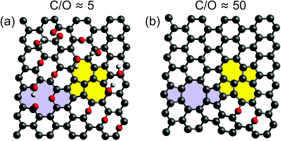 | ||
| Fig. 1 Schematic representation of functionalized graphene at different degrees of reduction as indicated. Besides the functionalization of the basal plane of graphene through epoxy and hydroxyl groups as well as ketones, also a divacancy (light violet) and a Stone–Wales defect (yellow) are shown as representative examples of lattice defects. The red dots indicate oxygen and light grey ones hydrogen atoms. | ||
While the chemical route produces a material with a lower number density of lattice defects, it is less effective than the thermal route in reducing the material. It is known that chemically reduced rGO typically exhibits an O/C ratio above 4.19%, corresponding to a C/O ratio x < 24.21 Directly exfoliated graphite – while showing a small level of defectiveness – contains almost no oxygen (x → ∞). FGS, however, can be tuned from a C/O ratio of x = 2 (no reduction) to values in excess of 500, thus approaching pristine graphene. Since the degree of thermal reduction determines the material's electrical properties, FGSs offer the unique possibility of tuning the electrical conductivity of the material from insulating over semi-conducting to conducting.19,20
However, for commercial applications of FGSs, the long-term stability of performance-determining material properties is essential. In particular in applications, where FGSs are exposed to the environment, e.g., to oxygen and humidity from the air, it is crucial to understand, how the environment may affect the electrical properties of FGSs and thus of the whole material system into which the FGSs have been incorporated.
Investigations of the effect of environment on the electronic properties of graphene have focused on mechanically exfoliated22,23 and chemical vapor-deposited (CVD)24–29 graphene. For example, Balandin's group investigated the electrical and noise characteristics of a field-effect transistor structure based of mechanically exfoliated graphene, when it was exposed to ambient conditions for over a month.22,23 They found an increase in noise with time, which was attributed to a decrease in carrier mobility and an increase of the contact resistances. For CVD graphene, Yavari et al. observed a saturation behaviour in the change of the resistance, when the graphene was exposed to humid air for 7.5 hours, and the time to reach the saturation dependent on the absolute humidity.24 In contrast, Pustelny et al. did not observe any saturation within 4 hours.26 A number of recent investigations discussed the stability of n- or p-doped CVD graphene. Xu et al. doped CVD graphene via adsorption of an organic compound (n type) and found stable values of the carrier mobility in air for up to 1000 hours.27 Using thermal treatment at 300 °C in an oxygen atmosphere, Piazza et al. obtained p-doping of graphene, which was stable even after a thermal treatment for up to 15 hours.28 Melios et al. showed that mono and bi-layer CVD graphene is extremely sensitive to water substances in controlled humidity environments.29
Much less is known about the influence of ambient atmosphere on the electrical properties of rGO30–33 or even FGS. Gómez-Navarro et al. found a significant shift of the Dirac-point to positive gate-source voltages VGS, when rGO was exposed to air atmosphere for 24 hours, which could be reversed by placing the graphene back in vacuum.30 Gupta et al. showed that during aging of polyethylene glycol-rGO composites for 3–6 months the number of oxygen-containing functional groups increases with time.33 Most important, no systematic studies of adsorption effects exist in case of FGSs (although expected to be similar to those obtained with rGO) and irreversible effects – leading to aging – have been largely neglected both in rGO and FGS.
In this work, we systematically analyze the long-term stability of the electronic properties of FGSs with different degrees of functionalization, using materials with C/O ratios between x = 5.4 and x = 60 under air and nitrogen atmosphere. Using a back-gate field effect transistor configuration, the doping level and the charge carrier mobility for FGSs can be determined separately. Our experiments give access to the impact of physisorbed and chemisorbed atmospheric species on the electronic properties of FGSs.
2. Experimental section
Preparation of FGSs
FGSs were prepared by thermal exfoliation of graphite oxide, as described in detail elsewhere.17,20 In short, individual graphene sheets are separated due to the gas evolution at high temperatures. Hereby the C/O ratio increases simultaneously due to the removal of oxygen.17 Depending on the temperature and the duration time of the exfoliation process, C/O ratios can be varied between 4 and 340.19,20 The samples used in this work were prepared with the following parameters: 300 °C for 1 min resulting in a C/O ratio of 5.4 ± 0.2, 500 °C for 1 min (C/O = 6 ± 0.3), 1100 °C for 1 min (C/O = 26 ± 2) and 1100 °C for 10 min (C/O = 60 ± 12).Device fabrication
To evaluate the electrical properties of a single FGS a standard back-gated field-effect transistor device architecture was used.2 Prior to processing, the FGS powders are stored under nitrogen atmosphere. For electrically contacting individual graphene sheets with typical sizes in the sub-μm range, a highly n-doped Si substrate with an insulating 90 nm SiO2 layer on top was pre-patterned with alignment marks (10 nm/50 nm Ti/Au) via electron beam lithography (Zeiss Supra 25) in order to subsequently define the positions of the sheets to be contacted relative to the marks. The FGSs were dispersed in ethanol (C/O ratios of 5.4, 6, and 26) or 1,2-dichloroethane (C/O ratio of 60), tip-sonicated (Bandelin Sonopuls HD 2070) at 21 W power centrifuged at 1073g for an hour each. Then the dispersion was drop-cast onto the pre-patterned substrate and dried at room temperature. After defining the positions with the help of the alignment marks, the contacts were designed by an Elphy Quantum lithography tool and patterned via electron beam lithography using 310 nm PMMA as a resist, which after exposure was developed with methyl isobutyl ketone (1 minute) and 2-propanol (1 minute) and blown dried under a nitrogen stream. 10 nm of Ti as an adhesion layer and 50 nm of Au was evaporated afterwards as contact materials (Oerlikon Leybold Vacuum Univex 350). The lift-off process was performed by leaving the sample in an acetone bath overnight and subsequent, gentle rinsing with 2-propanol, followed by blow-drying under a stream of nitrogen.Measurement and analysis procedure
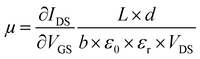
The electrical behavior of a single FGS can be characterized by the electrical current flowing from the drain to the source contact (IDS) in dependence of a drain-source voltage (VDS) and a gate-source voltage (VGS).2 These measurements (IDSvs. VDS resp. VGS) were conducted by applying a drain-source voltage VDS (Yokogawa GS 200) and measuring the drain-source current IDS with a current-to-voltage converter (Femto DLPCA-200) and a multimeter (Keithley 2000). To avoid damages to the FGSs and to exclude artifacts due to different applied currents in case of different C/O ratios, VDS was varied for each sample such that IDS did not exceed 150 nA. For each C/O ratio, the resistance was measured for 3 to 7 samples, and an average value and a standard deviation were calculated. To study the effect of aging, the IDS/VDS measurements were repeated each day for a period of about a week. Between the measurements, the samples were stored under laboratory air in a clean room (humidity of 40% at 20.5 °C). The measurements were conducted either under atmospheric conditions or under continuous nitrogen flow. The nitrogen flow was activated at least an hour prior to measurement, allowing the system to equilibrate. In addition, for the reference measurement the test specimens were kept under nitrogen flow for the whole duration of the long-term measurement.The gate-source voltage VGS was applied by a source meter (Keithley 2601A) through a copper foil attached to the backside of the silicon substrate. The field-effect dependence of the resistance was measured as a function of VGS. From the slope of the IDSvs. VGS curve the mobilities of the charge carriers are extracted using the equation34
 | (1) |
 | (2) |
 | (3) |
3. Results and discussion
The details about preparation methods and the measurement and analysis procedures are provided in the Experimental section. The samples with varied C/O ratio, x ranging from 5.4 to 60 were prepared as described in ref. 17 and 20. The C/O ratios were calculated from EDX measurements on pellets that are fabricated from powders with different exfoliation parameters and have been confirmed by CHNO analysis, giving a 1![[thin space (1/6-em)]](https://www.rsc.org/images/entities/char_2009.gif) :1 correlation. Exfoliation parameters and the resulting C/O ratios are shown in Table 1. Indicated errors represent the standard deviation obtained from measurements at different locations on pressed FGS powder pellets.
:1 correlation. Exfoliation parameters and the resulting C/O ratios are shown in Table 1. Indicated errors represent the standard deviation obtained from measurements at different locations on pressed FGS powder pellets.
| Exfoliation | C/O ratio x | Oxygen content in at% |
|---|---|---|
| 300 °C, 60 s | 5.4 ± 0.2 | 15.6 ± 0.6 |
| 500 °C, 60 s | 6 ± 0.3 | 14.3 ± 0.7 |
| 1100 °C, 60 s | 26 ± 2 | 3.7 ± 0.3 |
| 1100 °C, 600 s | 60 ± 12 | 1.6 ± 0.3 |
The IDS/VDS curves obtained for FGS with C/O ratios of x = 5.4 and x = 60 measured on different days under atmospheric environment and under nitrogen flow are shown in Fig. 2. The measurements were performed within identical current ranges for samples of different C/O ratios to ensure that observed differences are not caused by current-related artefacts. A non-linear behavior is apparent for x = 5.4 both under air [Fig. 2(a), top] and under nitrogen [Fig. 1(a), bottom] conditions, whereas the sample with a high C/O ratio of x = 60 shows a linear IDS/VDS dependence.20I/V curves for intermediate values of x fall in between those shown in Fig. 2.
 | ||
| Fig. 2 I DS/VDS characteristics of selected single FGS transistor devices for C/O ratios (a) x = 5.4 and (b) x = 60 under air (top) and N2 (bottom) atmosphere at different days. The gate of the device was left unconnected (floating gate). | ||
The change from non-linear to linear IDS/VDS behavior for low to high C/O ratios is comparable to what is reported in the literature and can be attributed to an increase of sp2-hybridized islands in a sp3-hybridized backbone with decreasing oxidation resulting in a change of the transport mechanism from mainly hopping to diffusive.20,30,38 For low C/O ratios the contacts might in addition contribute to the overall resistance.20 At a first glance, only a small variation of the I/V characteristics with atmosphere is found for both C/O ratios. Independent of the C/O ratio x, however, a pronounced decrease in the current at any given VDS is observed, when the measurements are repeated over a period of a few days.
Due to the partly non-linear nature of the current–voltage relation, we calculated the differential conductance at different current values (0, −100 nA, +90 nA). These data are normalized to the differential conductance measured on the first day, which is shown in Fig. 3(a) as a function of time. A decrease in the relative differential conductance is observed with aging time in all current regimes for x = 5.4 and x = 60 (inset), indicating that the aging is independent of the non-linearity of the I/V curves.
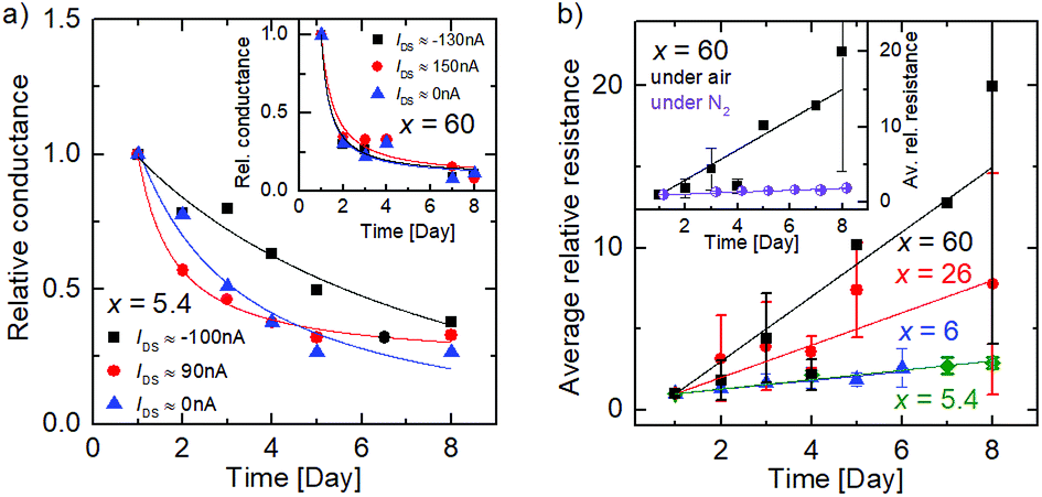 | ||
| Fig. 3 Time dependent aging of the FGSs (a) relative conductance vs. time for FGSs with C/O ratios of x = 5.4 and x = 60 (inset) (b) average relative resistance for different values x as a function of time under air. The inset compares data where the sample (x = 60) was stored in air or under nitrogen atmosphere, respectively, for the whole time. | ||
To discuss the C/O ratio-dependent aging, we calculated the relative differential resistance around IDS ≈ 0 A for different samples and plotted the average values as a function of time in Fig. 3(b). A clear increase in the relative resistance is shown due to aging, becoming more prominent as the C/O ratio increases. The resistance changes by about a factor of three for x = 5.4, whereas the resistance for x = 60 increases by more than an order of magnitude from day 1 to day 8. The resistance increase of the x = 6 sample is comparable to that observed for x = 5.4, and the value for x = 26 lies between both extrema. Thus, we observe an increase of resistance over time, whose relative amount increases with C/O ratio. Reference measurements, where the sample was strictly kept under nitrogen atmosphere for the whole time, were performed for x = 60 and can be seen in the inset of Fig. 3(b). The increase in resistance is negligible compared to the alteration under laboratory air indicating that the aging is caused solely by the atmospheric species. We attribute our observations to an aging of the FGSs rather than to a change of the metal/graphene contacts, because a contact resistance change, e.g., due to the oxidation of the Ti/Au contacts, should be virtually independent of the C/O ratio.
Since the resistance of the FGS sheets depends on both the charge carrier density and the carrier mobility, it is necessary to figure out the role of both during aging. For that purpose, we measured the IDS/VGS characteristic with varying back-gate voltages. By applying a back-gate voltage, the charge carrier density in the FGS changes and therefore the Fermi level shifts. Negative (positive) voltages induce holes (electrons) and shift the Fermi level accordingly.39
To study the atmospheric doping effect of FGSs with different C/O ratios, we performed measurements with varying gate-source voltages VGS under different environmental conditions and the results are shown in Fig. 4. Increasing the amount of functional groups, i.e., decreasing the C/O ratio x, the overall resistance increases both under air [Fig. 4(a)] and nitrogen atmosphere [Fig. 4(b)]. This trend agrees well with literature.20 We measure a Dirac point voltage of VGS0 ≥ 25 V under ambient conditions for all C/O ratios, indicating pronounced p-type doping for all types of FGSs. In contrast, VGS0 is shifted to about 0 V under N2 atmosphere. A similar behavior has been also reported in the literature for rGO,30 where it has been shown that under vacuum VGS0 is shifted close to zero. Within our experimental error, the back-gate voltage dependence under N2 atmosphere is almost symmetric for p- and n-type transport regimes.
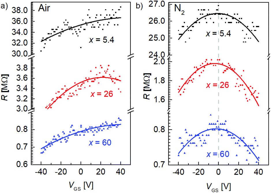 | ||
| Fig. 4 Electrical field-effect for FGSs with different C/O-ratios measured (a) under air and (b) under nitrogen atmosphere. | ||
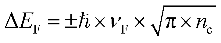
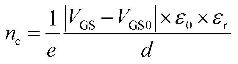
In contrast to pristine graphene, a parabolic behavior is observed in rGO and FGS close to Dirac point voltage rather than a linear relationship30,31 due to the large amount of scattering. We thus defined a fixed value of the charge carrier density (i.e., a fixed Fermi level, see Experimental section), in order to compare the mobility values of FGSs with varying C/O ratios and emphasize that the extracted values for charge carrier mobility should be understood as first approximations. We extracted the hole mobility from the data depicted in Fig. 4 at a Fermi level shift of ΔEF = −0.15 eV into the valence band, where we have a p-type transport, and the electron mobility at a value of ΔEF = 0.15 eV into the conduction band, yielding a n-type transport. The values obtained for the field-effect mobility for FGSs with different C/O ratios are extracted and summarized in Table 2 for ambient conditions and for nitrogen atmosphere. Due to high p-type doping under air the mobility of the electrons is not accessible. By decreasing the amount of oxygen from x = 5.4 to x = 60, the hole mobility is found to increase by roughly two orders of magnitude under ambient conditions. We obtain hole mobilities of μp = 0.16 × 10⁻³ cm2 V−1 s−1 for x = 5.4 and μp = 11 × 10−3 cm2 V−1 s−1 for x = 60. These values are in reasonable agreement with literature data found for rGO, where values of 0.01 cm2 V−1 s−1 to 1 cm2 V−1 s−1 are reported.38,40 The same trend for the hole mobility is apparent under nitrogen atmosphere, where the electron mobility can be extracted additionally. An electron mobility of μn = 0.06 × 10⁻³ cm2 V−1 s−1 is obtained for x = 5.4, increasing by a factor of 200 for x = 60.
| C/O ratio, x | Air [day 2] | Nitrogen [day 3] | |
|---|---|---|---|
| μ p 103 [cm2 V−1 s−1] | μ p 103 [cm2 V−1 s−1] | μ n 103 [cm2 V−1 s−1] | |
| 5.4 | 0.16 | 0.06 | 0.06 |
| 26 | 4 | 2.2 | 2.9 |
| 60 | 11 | 9 | 12 |
The measurement of the back-gate voltage dependence was repeated at different days for FGSs with a C/O ratio of x = 26 under air and nitrogen. From Fig. 5 it can be seen, that although a slight shift of the Dirac point voltage seems to occur under ambient atmosphere, the sample remains strongly p-doped after aging under ambient conditions. In addition, no shift of the Dirac point voltage is seen when the samples are measured under nitrogen atmosphere after different days of aging. This indicates that the Fermi energy changes only weakly as a result of the aging process.
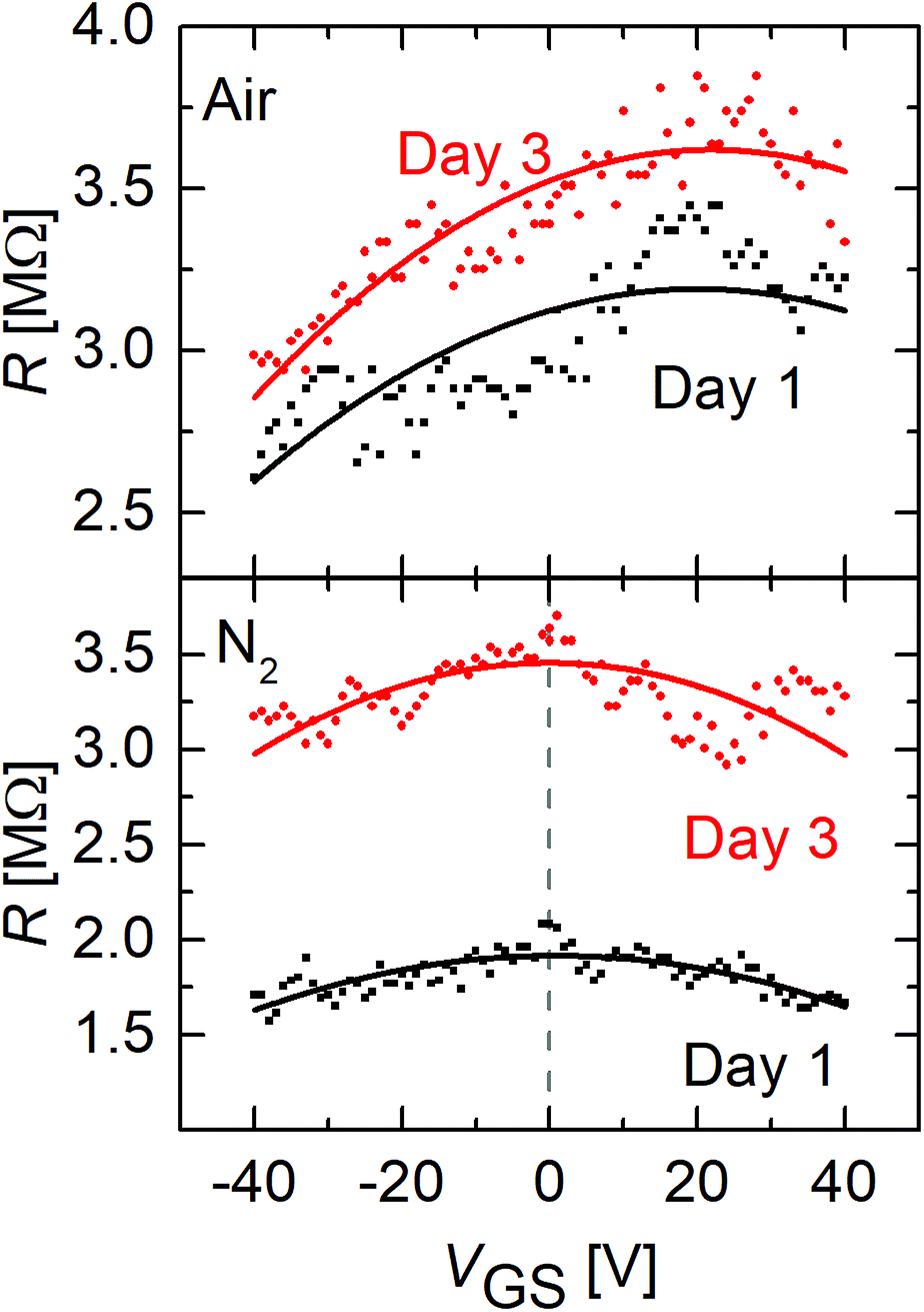 | ||
| Fig. 5 Resistance of FGS with a C/O ratio of x = 26 versus gate voltage for different days under air (top) and nitrogen (bottom) atmosphere. | ||
We thus conclude that the observed increase in resistance over the course of several days is caused by a decreasing mobility during aging. Agreeing with Gupta et al.33 the amount of functional groups and hence the amount of sp3-hybridization might increase during aging, resulting in an increased carrier scattering, limiting the electronic transport. We attribute this to incorporation (chemisorption) of adsorbing atmospheric species such as water and oxygen into the FGSs. This view can be supported by the fact that FGSs with x = 60 show the largest relative aging effect, as the material has been shown previously to be highly defective, while exhibiting only a comparably small number of oxygen-containing functional groups.41,42 Therefore, already a small amount of chemisorbing species can have a relatively large impact on the chemical structure and the electronic properties of the material.
4. Conclusions
In summary, we studied the electrical properties of single functionalized graphene sheets (FGSs) with varying amount of functional groups in a back-gated field-effect transistor device architecture. A reversible p-doping of FGSs as a result of exposure to ambient air is found for all C/O ratios. This can be attributed to an adsorption of atmospheric species, which can be removed under nitrogen atmosphere. Further, a significant increase in the resistance in an 8 days' time period is seen, when the samples are exposed to laboratory air, which is more prominent for larger C/O ratios. By determining separately the effect on the charge carrier density and the charge carrier mobility, we could distinguish between the (reversible) influence of adsorbed species from that of irreversible changes of the material due to chemisorption/oxidation. The latter one results in an alteration of the charge carrier mobility due to the chemisorbed oxygen containing atmospheric species, which serve as additional charge carrier scatterers.The change of electrical properties over time has significant importance in applications of FGS (and rGO), where the material is exposed to potentially reactive chemical environments. It must be expected that material performance may change over time, as the graphene material becomes successively more oxidized. Besides exposure to air, also the contact with other materials such as polymer matrices may cause effects of the kind observed here.
Conflicts of interest
C. P. and I. A. A. declare financial interest in Vorbeck Materials Corp., a manufacturer of FGS-based materials and products.Acknowledgements
We are gratefully thankful to Nicole Stracke, Maryan Barylyak and Piotr Sardyko for their experimental support. This work has been funded by the German Research Foundation (DFG) in the frame of the SPP 1459 “Graphene” under contract ME 1173/4-1.References
- K. S. Kim, Y. Zhao, H. Jang, S. Y. Lee, J. M. Kim, K. S. Kim, J.-H. Ahn, P. Kim, J.-Y. Choi and B. H. Hong, Nature, 2009, 457(7230), 706–710 CrossRef CAS.
- F. Schwierz, Nat. Nanotechnol., 2010, 5(7), 487–496 CrossRef CAS.
- X. Song, J. Hu and H. Zeng, J. Mater. Chem. C, 2013, 1(17), 2952 RSC.
- Z. Yu, L. Tetard, L. Zhai and J. Thomas, Energy Environ. Sci., 2015, 8(3), 702–730 RSC.
- F. Bonaccorso, L. Colombo, G. Yu, M. Stoller, V. Tozzini, A. C. Ferrari, R. S. Ruoff and V. Pellegrini, Science, 2015, 347(6217), 1246501 CrossRef.
- J. D. Roy-Mayhew, D. J. Bozym, C. Punckt and I. A. Aksay, ACS Nano, 2010, 4(10), 6203–6211 CrossRef CAS.
- D. A. C. Brownson, D. K. Kampouris and C. E. Banks, J. Power Sources, 2011, 196(11), 4873–4885 CrossRef CAS.
- M. A. Pope, S. Korkut, C. Punckt and I. A. Aksay, J. Electrochem. Soc., 2013, 160(10), A1653–A1660 CrossRef CAS.
- S. Stankovich, D. A. Dikin, G. H. B. Dommett, K. M. Kohlhaas, E. J. Zimney, E. A. Stach, R. D. Piner, S. T. Nguyen and R. S. Ruoff, Nature, 2006, 442(7100), 282–286 CrossRef CAS.
- T. Ramanathan, A. A. Abdala, S. Stankovich, D. A. Dikin, M. Herrera-Alonso, R. D. Piner, D. H. Adamson, H. C. Schniepp, X. Chen, R. S. Ruoff, S. T. Nguyen, I. A. Aksay, R. K. Prud'Homme and L. C. Brinson, Nat. Nanotechnol., 2008, 3(6), 327–331 CrossRef CAS.
- X. Huang, X. Qi, F. Boey and H. Zhang, Chem. Soc. Rev., 2012, 41(2), 666–686 RSC.
- L. Gan, F. Qiu, Y.-B. Hao, K. Zhang, Z.-Y. Zhou, J.-B. Zeng and M. Wang, J. Mater. Sci., 2016, 51(11), 5185–5195 CrossRef CAS.
- F. Qiu, Y. Hao, X. Li, B. Wang and M. Wang, Composites, Part B, 2015, 71, 175–183 CrossRef CAS.
- H. Liu, Y. Li, K. Dai, G. Zheng, C. Liu, C. Shen, X. Yan, J. Guo and Z. Guo, J. Mater. Chem. C, 2016, 4(1), 157–166 RSC.
- H. Liu, M. Dong, W. Huang, J. Gao, K. Dai, J. Guo, G. Zheng, C. Liu, C. Shen and Z. Guo, J. Mater. Chem. C, 2017, 5(1), 73–83 RSC.
- S. Stankovich, D. A. Dikin, R. D. Piner, K. A. Kohlhaas, A. Kleinhammes, Y. Jia, Y. Wu, S. T. Nguyen and R. S. Ruoff, Carbon, 2007, 45(7), 1558–1565 CrossRef CAS.
- M. J. McAllister, J.-L. Li, D. H. Adamson, H. C. Schniepp, A. A. Abdala, J. Liu, M. Herrera-Alonso, D. L. Milius, R. Car, R. K. Prud'homme and I. A. Aksay, Chem. Mater., 2007, 19(18), 4396–4404 CrossRef CAS.
- Y. Hernandez, V. Nicolosi, M. Lotya, F. M. Blighe, Z. Sun, S. De, I. T. McGovern, B. Holland, M. Byrne, Y. K. Gun'Ko, J. J. Boland, P. Niraj, G. Duesberg, S. Krishnamurthy, R. Goodhue, J. Hutchison, V. Scardaci, A. C. Ferrari and J. N. Coleman, Nat. Nanotechnol., 2008, 3(9), 563–568 CrossRef CAS.
- L. Yan, C. Punckt, I. A. Aksay, W. Mertin and G. Bacher, Nano Lett., 2011, 11(9), 3543–3549 CrossRef CAS.
- C. Punckt, F. Muckel, S. Wolff, I. A. Aksay, C. A. Chavarin, G. Bacher and W. Mertin, Appl. Phys. Lett., 2013, 102(2), 23114 CrossRef.
- M. Zhou, Y. Wang, Y. Zhai, J. Zhai, W. Ren, F. Wang and S. Dong, Chem.–Eur. J., 2009, 15(25), 6116–6120 CrossRef CAS.
- S. Rumyantsev, G. Liu, W. Stillman, M. Shur and A. A. Balandin, J. Phys.: Condens. Matter, 2010, 22(39), 395302 CrossRef CAS.
- M. Shur, S. Rumyantsev, G. Liu and A. A. Balandin, Proc. ICNF, 2011, vol. 21, pp. 145–149 Search PubMed.
- F. Yavari, C. Kritzinger, C. Gaire, L. Song, H. Gulapalli, T. Borca-Tasciuc, P. M. Ajayan and N. Koratkar, Small, 2010, 6(22), 2535–2538 CrossRef CAS.
- S. Ryu, L. Liu, S. Berciaud, Y.-J. Yu, H. Liu, P. Kim, G. W. Flynn and L. E. Brus, Nano Lett., 2010, 10(12), 4944–4951 CrossRef CAS PubMed.
- T. Pustelny, M. Setkiewicz, S. Drewniak, E. Maciak, A. Stolarczyk, M. Procek, M. Urbańczyk, K. Gut, Z. Opilski, I. Pasternak and W. Strupinski, Acta Phys. Pol., A, 2012, 122(5), 870–873 CrossRef CAS.
- W. Xu, T.-S. Lim, H.-K. Seo, S.-Y. Min, H. Cho, M.-H. Park, Y.-H. Kim and T.-W. Lee, Small, 2014, 10(10), 1999–2005 CrossRef CAS.
- A. Piazza, F. Giannazzo, G. Buscarino, G. Fisichella, A. La Magna, F. Roccaforte, M. Cannas, F. M. Gelardi and S. Agnello, J. Phys. Chem. C, 2015, 119(39), 22718–22723 CrossRef CAS.
- C. Melios, A. Centeno, A. Zurutuza, V. Panchal, C. E. Giusca, S. Spencer, S. R. P. Silva and O. Kazakova, Carbon, 2016, 103, 273–280 CrossRef CAS.
- C. Gómez-Navarro, R. T. Weitz, A. M. Bittner, M. Scolari, A. Mews, M. Burghard and K. Kern, Nano Lett., 2007, 7(11), 3499–3503 CrossRef.
- I. Jung, D. A. Dikin, R. D. Piner and R. S. Ruoff, Nano Lett., 2008, 8(12), 4283–4287 CrossRef CAS.
- C. W. Lee, B. J. Min, S. I. Kim and H. K. Jeong, Carbon, 2013, 54, 353–358 CrossRef CAS.
- B. Gupta, N. Kumar, K. A. Titovich, K. V. Ivanovich, S. A. Vyacheslavovich and S. Dash, Surf. Interfaces, 2017, 7, 6–13 CrossRef CAS.
- D. K. Schroder, Semiconductor Material and Device Characterization, John Wiley & Sons, Inc, Hoboken, NJ, USA, 1998 Search PubMed.
- S. Kim, I. Jo, D. C. Dillen, D. A. Ferrer, B. Fallahazad, Z. Yao, S. K. Banerjee and E. Tutuc, Phys. Rev. Lett., 2012, 108(11), 116404 CrossRef.
- H. Zhong, Z. Zhang, H. Xu, C. Qiu and L.-M. Peng, AIP Adv., 2015, 5(5), 57136 CrossRef.
- A. Das, S. Pisana, B. Chakraborty, S. Piscanec, S. K. Saha, U. V. Waghmare, K. S. Novoselov, H. R. Krishnamurthy, A. K. Geim, A. C. Ferrari and A. K. Sood, Nat. Nanotechnol., 2008, 3(4), 210–215 CrossRef CAS.
- C. Mattevi, G. Eda, S. Agnoli, S. Miller, K. A. Mkhoyan, O. Celik, D. Mastrogiovanni, G. Granozzi, E. Garfunkel and M. Chhowalla, Adv. Funct. Mater., 2009, 19(16), 2577–2583 CrossRef CAS.
- A. K. Geim and K. S. Novoselov, Nat. Mater., 2007, 6(3), 183–191 CrossRef CAS.
- A. Liscio, G. P. Veronese, E. Treossi, F. Suriano, F. Rossella, V. Bellani, R. Rizzoli, P. Samorì and V. Palermo, J. Mater. Chem., 2011, 21(9), 2924 RSC.
- M. A. Pope and I. A. Aksay, J. Phys. Chem. C, 2015, 119(35), 20369–20378 CrossRef CAS.
- J. D. Roy-Mayhew, M. A. Pope, C. Punckt and I. A. Aksay, ACS Appl. Mater. Interfaces, 2016, 8(14), 9134–9141 CrossRef CAS.
Footnote |
| † Present address: Institute of Nanotechnology, Karlsruhe Institute of Technology, 76344 Eggenstein-Leopoldshafen, Germany. |
| This journal is © The Royal Society of Chemistry 2018 |