
 Open Access Article
 This Open Access Article is licensed under a Creative Commons Attribution-Non Commercial 3.0 Unported Licence
Modification of dry/wet hybrid fabrication method for preparing a perovskite absorption layer on a PCBM electron transport layer†
Junta Kagae‡
,
Takaaki Yamanaka‡,
Shun Takahashi and
Kenichi Yamashita *
*
Faculty of Electrical Engineering and Electronics, Kyoto Institute of Technology, Matsugasaki, Sakyo-ku, Kyoto 606-8585, Japan. E-mail: yamasita@kit.ac.jp
First published on 20th November 2018
Abstract
The fabrication method of a perovskite absorption layer on a [6,6]-phenyl-C61-butyric acid methyl ester (PCBM) electron transport layer was investigated for application to perovskite/Si tandem photovoltaic devices. A dry/wet hybrid method that involves thermal evaporation of a PbI2 precursor followed by spin coating of an organic cation solution was found to be a useful means to form a perovskite layer without destruction of the underlying PCBM layer. To form the perovskite layer densely packed with crystals of large grain size and having smooth surface morphology, the rotational speed of the spin coating and the mixing ratio of organic cations were carefully modified. By using this modified absorption layer, a photovoltaic device fabricated under atmospheric exposure conditions showed a power conversion efficiency of ∼10.3% without any large hysteresis. These results have great importance to develop a production technology for high performance tandem solar cells.
Introduction
Lead halide perovskites have excellent optoelectronic functions and are thus promising materials for various electronic and photonic device applications such as solar cells,1–3 light-emitting diodes,4,5 and optically pumped lasers.6,7 One important application of these materials is their use as an absorption layer of a top cell in a tandem photovoltaic device with a crystal silicon (c-Si) bottom cell.8–13 Recent studies of the c-Si/perovskite tandem devices demonstrate that the power conversion efficiency (PCE) of ∼31% is theoretically possible, which is beyond the Shockley–Queisser limit defined in a single junction cell.8 Therefore the device architecture and fabrication methods of the c-Si/perovskite tandem solar cells should be investigated further to achieve better performance and to facilitate mass production.Recent studies have shown that one of the key factors for high performance tandem devices is the constitution of intermediate layers between the absorption layers of top and bottom cells, which engage in extraction, transport, and recombination of photoexcited carriers.10,11 Fullerene derivatives such as [6,6]-phenyl-C61-butyric acid methyl ester (PCBM) are useful candidates for an n-type carrier extraction layer that extracts electrons from the perovskite top cell and transports them to the recombination layer (e.g. a transparent intermediate electrode or the interface between highly doped p-type layer of the bottom cell and the n-type fullerene layer itself).11,14–17 This is because the PCBM can be deposited by a solution-based method at low temperature (<∼100 °C) without thermal damage of the Si bottom cells, which is in contrast with transparent conducting oxides requiring high temperature in their sintering procedure. In addition, a PCBM layer can extract efficiently photoexcited electrons from the perovskite absorption layer. Also its passivation effect on the perovskite layer causes a good electrical property without any significant hysteresis behavior.15–18 Therefore a fabrication scheme of the perovskite layer on the PCBM electron transport layer is important to realize tandem photovoltaic cells showing high PCE and stability.
To fabricate the perovskite layer on the PCBM layer successfully, a dry/wet hybrid method, that is thermal evaporation of lead iodide (PbI2) on PCBM (dry process) and following spin coating of methylammonium iodide (MAI) solution (wet process), has been used in recent studies.11,15,19,20 This hybrid method can avoid destructing the PCBM layer owing to the absence of direct exposure to perovskite precursor solutions. Therefore the PCBM layer can be introduced in the regular device configuration (i.e. an electron transport layer is at the bottom and a hole transport layer is at the top), which results in a high-quality perovskite layer as well as better electron extraction.15 Despite this large importance, however, there are few reports on systematic investigations of the film formation mechanism as well as on improvements in the fabrication recipe. In addition, fabrication under atmospheric exposure condition should also be investigated because this method would usually require sample transfers between the dry and wet processes.
In this study we studied on an improved dry/wet hybrid method for preparing a perovskite absorption layer on a planar PCBM electron transport layer. After deposition of PbI2 by thermal evaporation, we investigated the following wet process under atmospheric condition by comparing the spin coating method and dip coating one and by changing the rotational speed. Furthermore the impacts of formamidinium (FA) and MA cations mixing on the film formation were discussed in detail. Consequently a closely packed polycrystalline film, which was composed of grains in a ∼1 μm scale and showed a flat and pinhole-free surface morphology, was successfully fabricated. A planar-type photovoltaic device with this absorption layer showed an open circuit voltage as high as ∼1.0 V and a power conversion efficiency (PCE) of 10.3% without any large hysteresis.
Experimental
PCBM and poly(3-hexylthiophene-2,5-diyl) (P3HT) were purchased from Sigma-Aldrich. PbI2 and formamidinium iodide (FAI) were purchased from Tokyo Chemical, and MAI was purchased from Wako Pure Chemical. All chemicals were used as purchased from the suppliers. For preparation of the PCBM solution, PCBM powder was dissolved in chlorobenzene (CBz) with a concentration of 20 mg ml−1. The solution was stirred at room temperature for ∼1 hour. For preparation of the PbI2 precursor solution used in the wet process, N,N-dimethylformamide (DMF, 600 mg) was mixed with PbI2 powder (462.1 mg) and dimethylsulfoxide (DMSO, 70 mg), and the mixture was stirred at 70 °C for 1 hour for dissolution. The MAI precursor solution used for the spin coating was prepared by dissolving the MAI precursor (85 mg) into 2-propanol (1.0 ml). For MA/FA-mixed perovskite fabrications, the molar fraction of MAI/FAI was adjusted while keeping the total concentration constant. The prepared MAI (or MAI/FAI) precursor solution was stirred at 70 °C for 1 hour. For the MAI precursor solution used for the dip coating, the MAI precursor (200 mg) was dissolved in 2-propanol (20 ml) and the solution was stirred at 70 °C for 1 hour. For preparation of the P3HT solution, P3HT flakes were dissolved in CBz with a concentration of 40 mg ml−1. The solution was stirred at room temperature for ∼3 hours.Photovoltaic devices studied here have a layered structure of SiO2/fluorinated tin oxide (FTO)/compact (c-) TiO2/PCBM/FAxMA1−xPbI3/P3HT/Au. The c-TiO2 layer was deposited onto the FTO by the supplier (Solaronix). The SiO2/FTO/c-TiO2 substrate was cleaned with acetone and ethanol in an ultrasonic bath. The substrate was dried at 80 °C for 5 minutes and exposed to UV light for 20 minutes under ozone atmosphere to increase the hydrophilicity. Next PCBM was spin coated at 2000 rpm for 30 seconds and then annealed at 100 °C for 10 minutes on a hot plate. The resultant thickness of PCBM layer was 100 nm. To fabricate the perovskite absorption layer, the PbI2 precursor layer was deposited by thermal deposition or spin coating. In the thermal deposition, the vacuum level was 2 × 10⁻⁵ Torr, and the deposition rate and time were in ranges of 2–3 Å s−1 and 15–20 minutes, respectively. The deposition rate was monitored with a crystal oscillator. The resultant thickness of deposited PbI2 was ∼300 nm. In the spin coating, the film of PbI2 precursor was fabricated at 3000 rpm for 30 seconds. The PbI2 film was annealed at 70 °C for 5 minutes. Thereafter a perovskite film was formed by either spin coating or dip coating. In the spin coating, the MAI precursor or the MAI/FAI precursor was spun on the PbI2 layer at 4000 or 1300 rpm for 30 seconds. The MAPbI3 film was annealed at 100 °C for 5 minutes whereas the FAxMA1−xPbI3 film were sequentially annealed; the annealing at 150 °C for 10 min followed by that at 100 °C for 40 min. In the dip coating, the sample, on which the PbI2 layer was deposited, was immersed into the MAI precursor solution for 1 minute and then annealed at 70 °C for 30 minutes. The thickness of perovskite absorption layer after the synthesis was ∼700 nm. Onto the perovskite layer, the P3HT hole transport layer with a thickness of 150 nm was fabricated by the spin coating at 3000 rpm for 30 seconds. The substrate was dried at room temperature for 30 minutes. Finally a gold top electrode with a thickness of 60 nm was deposited by vacuum evaporation.
A scanning electron microscope (SEM, S-5200, Hitachi) was employed for the observation of surface morphologies. X-ray diffraction measurements were also performed (Rigaku, RINT-2500). The Cu-Kα line was used. The current density–voltage (J–V) characteristics were measured using a source meter (Model 2400, Keythley) and a solar simulator (XES-40SI, SAN-EI). The J–V curves under both the forward and reverse voltage scanning directions were recorded.
Results and discussion
First we show the availability of PbI2 thermal evaporation as a deposition method of the perovskite absorption layer onto the PCBM electron transport layer. For this investigation, surface morphology observations by SEM were performed for thermally-evaporated or spin-coated PbI2 layers (Fig. 1a and b) and perovskite layers obtained after reaction with MAI precursor solution (Fig. 1c and d). As shown in Fig. 1a, the PCBM surface was found to be covered with crystalline PbI2 nanoplates deposited by thermal evaporation, while the PbI2 film formed by the spin coating (see Fig. 1b) is more amorphous. For these PbI2 films, MAI precursor solution was spin-coated to form MAPbI3 absorption layers at 4000 rpm. As shown in Fig. 1c, the surface morphology of MAPbI3 formed by the PbI2-evaporation is closely packed by tile-shaped crystals with the dimensions of 150–300 nm. On the other hand, the morphology of MAPbI3 formed by the PbI2-spin coating shows clustered crystals with the dimensions of 100–200 nm (see Fig. 1d). It is apparent that the surface flatness in Fig. 1c is much better than that in Fig. 1d. These results clearly show that formation of a MAPbI3 layer is largely affected by a pre-deposited PbI2 precursor. Also the porous structure observed in the thermally evaporated PbI2 film possibly promotes the reaction with MAI precursors. This would also affect the degree of crystallinity in the MAPbI3 crystals. These results demonstrate that the PbI2 thermal evaporation is one of the available means for preparing the MAPbI3 absorption layer on the PCBM electron transport layer. More importantly, we confirmed that the PbI2-spin coating degrades the photovoltaic performance significantly due to the destruction of the underlying PCBM layer (see Fig. S1 in the ESI†). This is not the case in the deposition scheme, as shown in the following. | ||
| Fig. 1 SEM images of PbI2 precursor films prepared by (a) vapour deposition method and (b) spin coating method. (c) and (d) SEM images of MAPbI3 perovskite films prepared by MAI spin coating from the PbI2 films of (a) and (b), respectively. | ||
We also investigated a dip coating method as the means to prepare the MAPbI3 perovskite layer from the evaporated PbI2 (see Fig. S2a in the ESI†). It is apparent that, as compared to the layer prepared by the spin coating (Fig. 1c), the grain size is smaller (130–200 nm) and the growth mode is more ‘three-dimensional’. This crystal growth mode would be due to the too rapid reaction of PbI2 with MAI. As shown in Fig. S2b in the ESI,† X-ray diffraction (XRD) intensity of the MAPbI3 prepared by the dip coating was as small as one half of that prepared by the spin coating. This result implies that the rapid reaction by the dip coating disturbs homogenous growth of the perovskite crystals. To make matter worse, the immersion time in the dip coating method was limited up to 1 minute because the peeling off of the film from the PCBM underlayer (soluble to the solvent) must be avoided. Namely, we can find that the MAI precursor volume and reaction rate are uncontrollable in the dip coating method.
When we introduced the method of MAI spin coating, on the other hand, the rotational speed was found to be an effective parameter to control them. As shown in a wide-area SEM image of Fig. 2a, the MAPbI3 surface after the spin coating at 4000 rpm still includes residual clustered PbI2. This would be due to the lack of MAI precursor and/or the too short reaction time. When the spin speed was reduced to 1300 rpm (see Fig. 2b), the volume of residual PbI2 was further decreased because of the further promotion in reaction and thus the grain size was also enlarged from ∼100 nm to ∼300 nm. By using this recipe, we were able to form a MAPbI3 film without significant degradation at the PCBM interface, which was confirmed in the photovoltaic performance as described later.
 | ||
| Fig. 2 Wide-area SEM images of MAPbI3 films prepared by spin coating of MAI precursor solution at (a) 4000 and (b) 1300 rpm. (c) and (d) SEM images of FA0.25MA0.75PbI3 films prepared by FAI/MAI spin coating at 4000 and 1300 rpm, respectively. | ||
Next let us see cases of FAPbI3/MAPbI3-mixed perovskite films. We fabricated FAxMA1−xPbI3 films with x = 0, 0.2, 0.25, and 0.5 by the spin coating of FAI/MAI mixed precursor solution on the evaporated PbI2. As shown in Fig. S3 in the ESI,† the films only with x = 0 (MAPbI3) or 0.25 (FA0.25MA0.75PbI3) were successfully fabricated. The yellow and orange films at x = 0.2 or 0.5 are due to the bleaching of perovskite and the appearance of δ-phase perovskite, respectively.21 These results show an importance of molar fraction ratio to enhance perovskite stability,22–25 especially under the ambient condition. Fig. 2c and d show wide-area SEM images of the FA0.25MA0.75PbI3 films. It is apparent that the average grain size of crystals increases by introducing FAI, as reported in a previous paper.25 When the schemes of low-speed spin coating and FA/MA mixing were combined (see Fig. 2d), the grain size of crystal was enlarged further to ∼1 μm. The large grains lead to the closely-packed and almost pinhole-free perovskite film formation. The film quality obtained here is comparable with a case of dual-source thermal deposition method.26 A possible mechanism for the high-quality film formation by the FA/MA mixing is the formation of stable cubic perovskite.25 We also performed XRD measurement as shown in Fig. 3. The (110) diffraction peak intensity of the FA0.25MA0.75PbI3 was ∼1.2 times larger than that of MAPbI3, demonstrating that the crystallinity is also further improved by the FA/MA mixing.
 | ||
| Fig. 3 XRD patterns of FA0.25MA0.75PbI3 and MAPbI3 films prepared by spin coating of precursor solutions at 1300 rpm. | ||
Finally we show photovoltaic characteristics of a solar cell device where the perovskite absorption layer was fabricated by the hybrid method described above. Fig. 4a and b shows the device structure and the appearance. PCBM and P3HT were used as the electron and hole transport layers (ETL and HTL), respectively. Fig. 4c shows current density–voltage (J–V) properties under dark condition and AM 1.5G illumination for the best performance device fabricated by the PbI2-thermal evaporation and the FAI/MAI-spin coating at 1300 rpm (corresponding to the sample of Fig. 2d). The J–V curve at the reverse scan shows a filling factor (FF) of 0.67 without pronounced hysteresis characteristics. The short-circuit current density Jsc and the open-circuit voltage Voc are 15.2 mA cm−2 and 1.02 V, respectively. As a result, the PCE of 10.3% is achieved. For comparison, we also measured J–V properties for the devices fabricated by the MAI-spin coating at 1300 rpm (corresponding to Fig. 2b) and that fabricated by the FAI/MAI-spin coating at 4000 rpm (corresponding to Fig. 2c). These results are shown in Fig. S4 in the ESI† and summarized in Table 1. The enhancement in Jsc by the FA/MA mixing (from 6.48 to 15.2 mA cm−2) is mainly due to the improvement of the perovskite crystallinity. Also, as compared Fig. 2c with 2d, the enhancement in Jsc by controlling the spin speed (from 2.29 to 15.2 mA cm−2) is caused by the enlargement of the average crystal grain size. Voc did not show significant variation among the samples, demonstrating the well stabilized recombination losses at the ETL/perovskite and perovskite/HTL interfaces. A stability test was performed for a device fabricated by FAI/MAI-spin coating at 1300 rpm as shown in Fig. S5 in the ESI.† The initial performance as large as ∼6% in PCE was improved to >10% after one day. A possible reason of this improvement is the slow evaporation of high boiling point solvents (CBz, DMF, and DMSO). After two days later, the device exhibited degradation in FF and increase in the hysteresis characteristic. While these negative features should be improved, the performance obtained in the reversed scan shows high stability even after 1 week (∼8% in PCE).
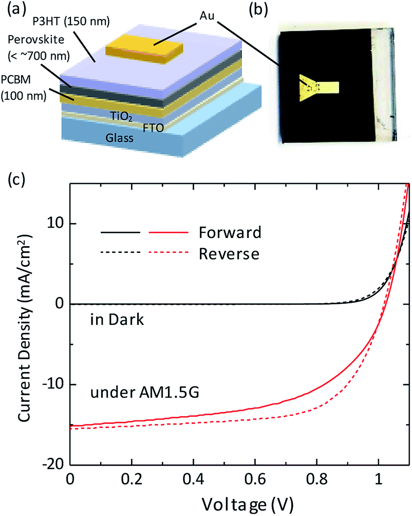 | ||
| Fig. 4 (a) A schematic of photovoltaic device structure. Detailed fabrication procedures and thickness of each layer are shown in Experimental section. (b) Overview image of photovoltaic sample. (c) Typical current density–voltage (J–V) curves for a photovoltaic device with FA0.25MA0.75PbI3 absorption layer prepared by FAI/MAI spin coating at 1300 rpm onto thermally evaporated PbI2. Black and red curves show the J–V characteristics in dark and under AM1.5G, respectively. Solid and dashed curves exhibit the data at forward and reverse scans in the voltage. | ||
| Jsc (mA cm−2) | Voc (V) | FF | PCE (%) | ||
|---|---|---|---|---|---|
| MAPbI3 (1300 rpm) | Forward | −7.28 ± 0.86 | 1.03 ± 0.01 | 0.51 ± 0.11 | 3.78 ± 0.29 |
| Reverse | −8.47 ± 2.02 | 1.04 ± 0.02 | 0.61 ± 0.06 | 5.46 ± 0.75 | |
| FA0.25MA0.75PbI3 (4000 rpm) | Forward | −2.23 ± 0.06 | 1.00 ± 0.02 | 0.48 ± 0.04 | 1.06 ± 0.03 |
| Reverse | −2.15 ± 0.13 | 1.02 ± 0.01 | 0.57 ± 0.01 | 1.26 ± 0.10 | |
| FA0.25MA0.75PbI3 (1300 rpm) | Forward | −14.94 ± 2.49 | 0.99 ± 0.03 | 0.51 ± 0.05 | 7.63 ± 1.29 |
| Reverse | −16.18 ± 3.09 | 0.97 ± 0.05 | 0.62 ± 0.04 | 9.59 ± 1.32 | |
| (Best sample) | Forward | −15.7 | 1.02 | 0.53 | 8.54 |
| Reverse | −15.2 | 1.02 | 0.67 | 10.3 |
It should be noted that all the device fabrications in this study, except for the thermal evaporation, were intentionally processed under the atmospheric exposure conditions (Rh ∼ 40–60%). Furthermore the devices were not encapsulated. Even so, the PCE larger than 10% was found to be possible. This result would not be so bad because PCEs of devices with the similar compositional ratio (20–30% of FA) are reported to be in a range of 17–19% when the device were fabricated in a grove box filled with nitrogen and encapsulated in measurements.25 Furthermore this method would be improved further by optimizing the mixing schemes, e.g. hybridization with the caesium iodide and lead bromide as similar to a very recent study.27 Such the optimization will provide the enhanced device performance of the perovskite top cell together with the production feasibility under atmospheric exposure conditions, which is important to achieve high-performance tandem solar cell modules and to develop their mass production technologies.
Conclusions
We investigated a hybrid dry/wet fabrication procedure for preparing a perovskite absorption layer onto a planar PCBM electron transport layer for applications to tandem photovoltaic devices. It was confirmed that thermal evaporation of PbI2 is available to form a densely packed perovskite layer without destruction of the underlying PCBM layer. To prepare a MAPbI3 layer from the PbI2 precursor film, the spin coating of MAI precursor solution at a slow rotational speed (∼1300 rpm) resulted in a smooth surface morphology without residual PbI2 clusters owing to the well-controlled MAI precursor volume and reaction rate. When FAI was mixed into the perovskite absorption layer, furthermore, average grain size of the perovskite crystal was enlarged to ∼1 μm and the density of the grain boundary was significantly decreased. A photovoltaic device composed of this improved absorption layer showed a power conversion efficiency of ∼10.3% without any large hysteresis. It should be noted that the fabricated device has undergone the atmospheric exposure processes. Therefore these findings will provide important information to develop the production technologies of perovskite/Si tandem solar cell.Conflicts of interest
There are no conflicts to declare.Acknowledgements
K. Y. thanks to JSPS KAKENHI Grant No. 15H03974 and 18H01476.Notes and references
- A. Kojima, K. Teshima, Y. Shirai and T. Miyasaka, J. Am. Chem. Soc., 2012, 131, 6050–6051 CrossRef PubMed.
- M. M. Lee, J. Teuscher, T. Miyasaka, T. N. Murakami and H. J. Snaith, Science, 2012, 338, 643–647 CrossRef CAS PubMed.
- H.-S. Kim, C.-R. Lee, J.-H. Im, K.-B. Lee, T. Moehl, A. Marchioro, S.-J. Moon, R. Humphry-Baker, J.-H. Yum, J. E. Moser, M. Grätzel and N.-G. Park, Sci. Rep., 2012, 2, 591 CrossRef PubMed.
- Z.-K. Tan, R. S. Moghaddam, M. L. Lai, P. Docampo, R. Higler, F. Deschler, M. Price, A. Sadhanala, L. M. Pazos, D. Credgington, F. Hanusch, T. Bein, H. J. Snaith and R. H. Friend, Nat. Nanotechnol., 2014, 9, 687–692 CrossRef CAS PubMed.
- H. Cho, S. u-H. Jeong, M.-H. Park, Y.-H. Kim, C. Wolf, C.-L. Lee, J. H. Heo, A. Sadhanala, N. S. Myoung, S. Yoo, S. H. Im, R. H. Friend and T.-W. Lee, Science, 2015, 350, 1222–1225 CrossRef CAS PubMed.
- F. Deschler, M. Price, S. Pathak, L. E. Klintberg, D.-D. Jarausch, R. Higler, S. Hüttner, T. Leijtens, S. D. Stranks, H. J. Snaith, M. Atatüre, R. T. Phillips and R. H. Friend, J. Phys. Chem. Lett., 2014, 5, 1421–1426 CrossRef CAS PubMed.
- G. Xing, N. Mathews, S. S. Lim, N. Yantara, X. Liu, D. Sabba, M. Grätzel, S. Mhaisalkar and T. C. Sum, Nat. Mater., 2014, 13, 476–480 CrossRef CAS PubMed.
- G. E. Eperon, M. T. Hörantner and H. J. Snaith, Metal halide perovskite tandem and multiple-junction photovoltaics, Nat. Rev. Chem., 2017, 1, 0095 CrossRef CAS.
- P. Löper, S.-J. Moon, S. M. de Nicolas, B. Niesen, M. Ledinsky, S. Nicolay, J. Bailat, J.-H. Yum, S. De Wolfa and C. Ballifa, Phys. Chem. Chem. Phys., 2015, 17, 1619–1629 RSC.
- J. P. Mailoa, C. D. Bailie, E. C. Johlin, E. T. Hoke, A. J. Akey, W. H. Nguyen, M. D. McGehee and T. Buonassisi, Appl. Phys. Lett., 2015, 106, 121105 CrossRef.
- J. Werner, C.-H. Weng, A. Walter, L. Fesquet, J. P. Seif, S. De Wolf, B. Niesen and C. Ballif, J. Phys. Chem. Lett., 2016, 7, 161–166 CrossRef CAS PubMed.
- K. A. Bush, A. F. Palmstrom, Z. J. Yu, M. Boccard, R. Cheacharoen, J. P. Mailoa, D. P. McMeekin, R. L. Z. Hoye, C. D. Bailie, T. Leijtens, I. Marius Peters, M. C. Minichetti, N. Rolston, R. Prasanna, S. Sofia, D. Harwood, W. Ma, F. Moghadam, H. J. Snaith, T. Buonassisi, Z. C. Holman, S. F. Bent and M. D. McGehee, Nat. Energy, 2017, 2, 17009 CrossRef CAS.
- F. Sahli, J. Werner, B. A. Kamino, M. Bräuninger, R. Monnard, B. Paviet-Salomon, L. Barraud, L. Ding, J. J. Diaz Leon, D. Sacchetto, G. Cattaneo, M. Despeisse, M. Boccard, S. Nicolay, Q. Jeangros, B. Niesen and C. Ballif, Nat. Mater., 2018, 17, 820–826 CrossRef CAS PubMed.
- C. Tao, S. Neutzner, L. Colella, S. Marras, A. R. S. Kandada, M. Gandini, M. De Bastiani, G. Pace, L. Manna, M. Caironi, C. Bertarelli and A. Petrozza, Energy Environ. Sci., 2015, 8, 2365–2370 RSC.
- F. Fu, T. Feurer, T. Jänger, E. Avancini, B. Bissig, S. Yoon, S. Bucheler and A. N. Tiwari, Nat. Commun., 2015, 6, 8932 CrossRef CAS PubMed.
- J. H. Kim, C.-C. Chueh, S. T. Williams and A. K.-Y. Jen, Nanoscale, 2015, 7, 17343–17349 RSC.
- L. Kegelmann, C. M. Wolff, C. Awino, F. Lang, E. L. Unger, L. Korte, T. Dittrich, D. Neher, B. Rech and S. Albrecht, ACS Appl. Mater. Interfaces, 2017, 9, 17245–17255 CrossRef CAS PubMed.
- A. H. Ip, L. N. Quan, M. M. Adachi, J. J. McDowell, J. Xu, D. H. Kim and E. H. Sargent, Appl. Phys. Lett., 2015, 106, 143902 CrossRef.
- F. Fu, L. Kranz, S. Yoon, J. Löckinger, T. Jänger, J. Perrenoud, T. Feurer, C. Gretener, S. Buecheler and A. N. Tiwari, Phys. Status Solidi A, 2015, 212, 2708–2717 CrossRef CAS.
- H. A. Abbas, R. Kottokkaran, B. Ganapathy, M. Samiee, L. Zhang, A. Kitahara, M. Noack and V. L. Dalal, APL Mater., 2015, 3, 016105 CrossRef.
- J. Dai, Y. Fu, L. H. Manger, M. T. Rea, L. Hwang, R. H. Goldsmith and S. Jin, J. Phys. Chem. Lett., 2016, 7, 5036–5043 CrossRef CAS PubMed.
- N. Pellet, P. Gao, G. Gregori, T.-Y. Yang, M. K. Nazeeruddin, J. Maier and M. Grätzel, Angew. Chem., Int. Ed., 2014, 53, 3151–3157 CrossRef CAS PubMed.
- N. J. Jeon, J. H. Noh, W. S. Yang, Y. C. Kim, S. Ryu, J. Seo and S. I. Seok, Nature, 2015, 517, 476–480 CrossRef CAS PubMed.
- F. Ji, L. Wang, S. Pang, P. Gao, H. Xu, G. Xie, J. Zhang and G. Cui, J. Mater. Chem. A, 2016, 4, 14437–14443 RSC.
- Y. Zhang, G. Grancini, Y. Feng, A. M. Asiri and M. K. Nazeeruddin, ACS Energy Lett., 2017, 2, 802–806 CrossRef CAS.
- M. Liu, M. B. Johnston and H. J. Snaith, Nature, 2013, 501, 395–398 CrossRef CAS PubMed.
- T. Singh and T. Miyasaka, Adv. Energy Mater., 2018, 8, 1700677 CrossRef.
Footnotes |
| † Electronic supplementary information (ESI) available. See DOI: 10.1039/c8ra08022d |
| ‡ J. K. and T. Y. contributed equally. |
| This journal is © The Royal Society of Chemistry 2018 |