
 Open Access Article
 This Open Access Article is licensed under a Creative Commons Attribution-Non Commercial 3.0 Unported Licence
Hydrogen evolution from silicon nanowire surfaces†
Rui Feng‡
 ,
Yang Liu‡,
Shipu Li,
Hanbin Chen,
Chengyi Song,
Peng Tao,
Jianbo Wu,
Peng Zhang,
Tao Deng* and
Wen Shang*
,
Yang Liu‡,
Shipu Li,
Hanbin Chen,
Chengyi Song,
Peng Tao,
Jianbo Wu,
Peng Zhang,
Tao Deng* and
Wen Shang*
State Key Laboratory of Metal Matrix Composites, School of Materials Science and Engineering, Shanghai Jiao Tong University, 800 Dong Chuan Road, Shanghai 200240, P. R. China. E-mail: dengtao@sjtu.edu.cn; shangwen@sjtu.edu.cn
First published on 12th December 2018
Abstract
This paper presents the study on the hydrogen evolution reaction (HER) of the silicon nanowire (SiNW)-based surfaces. Large-area SiNWs with different lengths were fabricated on the silicon surfaces by a cost effective and scalable wet-etching method. The SiNW-based surfaces promoted the photoelectrocatalytical performance of the electrodes due to the increased effective surface area for electrolyte diffusion and the fast release of hydrogen bubbles that formed on the electrodes. In addition, at different applied potentials, the nanostructured electrodes showed different behaviour that depended on the SiNWs' with different lengths and morphologies. For example, surfaces with longer SiNWs performed better in the low potential region, while surfaces with shorter SiNWs presented improved performance in the high potential region. The findings in this study provide new insights into designing electrodes with desired nanostructures for improved HER performance.
Introduction
The formation and release of bubbles from the solid–liquid interfaces are commonly observed phenomena during the boiling process or gas evolution on the electrodes in electrochemical or photoelectrochemical processes. The formation and release of the bubbles on the surface are critical to the performance of the systems. For example, the fast departure of the vapour bubbles from the heated surface can enhance the efficiency of the heat transfer process. In the electrochemical gas evolution reactions, the adhesion of the as-formed gas bubbles on the electrode surfaces blocks the diffusion of reactants and leads to the decrease in electrolysis or photoelectrocatalytic efficiency.1–12 Fast departure of the generated gas bubbles can also help increase the efficiency of such processes.Recently, it has been demonstrated that the microscale and nanoscale structures formed on the solid surfaces caused different surface wettability and influenced the adhesion and release of the bubbles generated on the surface.13–17 Jiang et al. reported that nanopine-shaped Pt electrodes showed improved H2 evolution performance due to the low bubble adhesion force and small bubble releasing size enabled by the nanostructure.18 In addition, they also reported the “superaerophobic” nanoporous MoS2 electrode that enabled rapid departure of the as-formed gas bubbles and improved the electrocatalytic performance.19 The nanostructures present on photocathode also improved the solar absorbance and significantly increased the solar hydrogen generation during the photoelectrochemical water splitting reaction.20–24 Regarding the pool boiling on the surfaces, Cheng et al. showed that both microstructures and nanostructures could enhance the heat transfer during the boiling process.25 The microstructures provided ample bubble nucleation sites and an effective heat transfer area to boost the heat flux at the low heat flux regime, while the nanostructures promoted the heat flux mainly through the decrease in bubble departure diameter and the acceleration of bubble departure frequency.
These previous efforts demonstrated the advantages of introducing micro/nanostructures on the bubble generation surfaces. However, there is still a lack of understanding of the exact correlation between the morphology of nanostructures and the efficiency of bubble generation and their release on the nanostructured surfaces. In this work, we intended to study the nucleation, growth, and release of H2 bubbles that were generated on Si nanowire (SiNW) surfaces during the photoelectrocatalytic water splitting process. SiNWs of ∼200 nm diameter and different lengths were fabricated on the silicon surface through wet-etching method26 and used as the electrodes for this study. With direct observation of the H2 bubbles by a high-speed camera, we found that SiNWs promoted the liberation of H2 bubbles from the electrode surfaces in comparison with that from the flat Si surface. In addition, detailed analysis revealed the correlation between the performance of hydrogen evolution at different applied potentials and the morphology of the SiNWs with various lengths. This study offers new insights into the bubble nucleation, growth, and release at the SiNW surfaces as well as the understanding of the relationship between photoelectrochemical performance and the SiNWs nanostructures.
Materials and methods
Material
Boron-doped p-type silicon wafers with diameter of 100 mm, thickness of 500 μm, and orientation of 〈100〉 were used for this study. The resistivity of the wafers was between 5 and 15 Ω cm. Silver nitrate (AgNO3, 99.99% metals basis) was obtained from Aladdin (Shanghai, China). Acetone, ethyl alcohol, sulfuric acid (H2SO4, 95–98%), hydrogen peroxide (H2O2, ≥30%), and hydrofluoric acid (HF, ≥40%) were obtained from Sinopharm Chemical Reagent Co., Ltd (Shanghai, China). All the chemicals were of analytical grade and used without further purification. Deionized (DI) water was produced by Millipore Water Purification System (NANO pure, Billerica, MA, USA, 18.2 MΩ).Fabrication of SiNWs through electroless chemical etching
Large-area SiNW-based surfaces were prepared through electroless wet chemical etching method. First, the Si wafers were cleaned ultrasonically for 10 minutes with acetone, ethanol and DI water, successively. The cleaned silicon wafers were immersed in the mixed solution of sulfuric acid/hydrogen peroxide (97% H2SO4/30% H2O2, 4![[thin space (1/6-em)]](https://www.rsc.org/images/entities/char_2009.gif) :1 v/v) for about 10 minutes to remove the surface impurities; then, the wafers were thoroughly rinsed with DI water. Subsequently, the samples were immersed into the diluted (1 wt%) hydrofluoric (HF) acid solution for 1 minute and washed thoroughly. The freshly treated samples were then immersed for 1 minute in the aqueous solution comprising 10−2 mol L−1 silver nitrate and 4.6 mol L−1 HF solution to deposit Ag nanoparticles on the surface. Subsequently, the samples were immersed in H2O2 (0.44 M)/HF (4.6 M) solution for further etching process. To obtain SiNWs with different lengths, the etching time was varied from 5 to 60 minutes. At last, the samples were immersed in concentrated nitric acid (HNO3) for ∼1 hour to remove the Ag particles from the samples. All the samples were rinsed with DI water thoroughly, followed by drying in air at room temperature. In addition, a planar silicon wafer was also cleaned and used as the control.
:1 v/v) for about 10 minutes to remove the surface impurities; then, the wafers were thoroughly rinsed with DI water. Subsequently, the samples were immersed into the diluted (1 wt%) hydrofluoric (HF) acid solution for 1 minute and washed thoroughly. The freshly treated samples were then immersed for 1 minute in the aqueous solution comprising 10−2 mol L−1 silver nitrate and 4.6 mol L−1 HF solution to deposit Ag nanoparticles on the surface. Subsequently, the samples were immersed in H2O2 (0.44 M)/HF (4.6 M) solution for further etching process. To obtain SiNWs with different lengths, the etching time was varied from 5 to 60 minutes. At last, the samples were immersed in concentrated nitric acid (HNO3) for ∼1 hour to remove the Ag particles from the samples. All the samples were rinsed with DI water thoroughly, followed by drying in air at room temperature. In addition, a planar silicon wafer was also cleaned and used as the control.
Morphology characterization
The morphologies of the SiNWs with different etching time were examined by Field-Emission Scanning Electron Microscopy (FESEM, FEI Sirion 200, 5 kV). The relationship between the lengths of the SiNWs and the corresponding etching time was obtained based on the statistical analysis.Photoelectrochemical (PEC) measurement
The schematic of the experimental setup is shown in Fig. 1. All electrochemical measurements were performed in a three-electrode configuration using a CHI600E/700E electrochemical workstation (CH Instruments, Inc., Shanghai, China). The planar Si wafer and SiNW samples were used as photocathodes and tested at room temperature in a custom-built quartz glass vessel filled with 0.5 M sulfuric acid electrolyte. A saturated calomel electrode (SCE) was used as the reference electrode and Pt plate was used as the counter electrode. The whole system was exposed to a simulated solar light (1000 W m−2) that was generated by a 300 W Xeon lamp (Shanghai Bilon Instrument Co., Ltd). Linear sweep voltammetry (LSV) curves were measured from +0.5 V to −2.0 V vs. SCE at a scan rate of 0.1 V s−1. Each curve was measured five times and the final sweep was used for the analysis.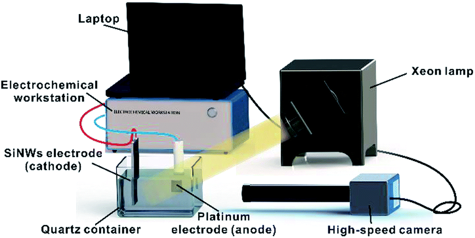 | ||
| Fig. 1 Schematic of the experimental setup. The SiNW electrode (cathode) and Pt electrode (anode) were vertically placed in a quartz container with 0.5 M sulphuric acid. The SiNW electrode was illuminated by a Xeon lamp. The electrodes were connected to the electrochemical workstation. The process of HER was captured by a high-speed camera. | ||
A high-speed camera (S-VIT LS, AOS Technologies AG, Switzerland) was used to record the dynamic behaviours of H2 bubbles generated on the surfaces of different samples. The videos were recorded as AVI files, with a recording speed of 200 frames per second and the resolution of 500 × 500 pixels. Statistic calculations of the bubble nucleation densities and sizes were processed using the recorded videos. The active nucleation site density of H2 bubbles and the departure sizes of H2 bubbles from different samples were calculated using image processing tool.
Results and discussion
The characterization of the morphologies of SiNWs
In this study, we fabricated nanostructured electrodes with SiNWs of different lengths through controlling the etching time. Fig. 2 provides both cross-sectional and top-down SEM images of the obtained NWs with different etching times. When the etching time changed from 10 minutes to 20 minutes and to 40 minutes, the lengths of the NWs increased from 1.48 ± 0.09 μm to 4.60 ± 0.41 μm and to 7.92 ± 0.62 μm, respectively (Fig. 2a, d, g and j). In the following discussion, we named these SiNW samples as 1.5 μm-SiNWs, 4.6 μm-SiNWs and 7.9 μm-SiNWs. Under the experimental conditions used in this study, the average etching rate was calculated to be ∼0.2 μm min−1, which is consistent with that obtained in the previous studies.27,28 Moreover, the diameter of the NWs almost remained constant for all the samples (∼200 nm) even with the increase in the etching time. Interestingly, these NWs were not individually aligned on the surface. Instead, they assembled into conical-shaped NW clusters on the surface with micro-pores among the clusters. The shapes of the micro-pores were irregular, while their size increased from sub-micrometer to several micrometers with the increase in the NW lengths. The average sizes of the micropores were about 0.82 ± 0.18 μm, 2.36 ± 0.38 μm, and 4.07 ± 0.78 μm for the samples etched for 10 minutes, 20 minutes, and 40 minutes, respectively. The formation of such SiNW clusters and micro-pores was mostly attributed to the effect of capillary force of water during the drying step.29 The hierarchical morphologies of the SiNWs on the surface were relatively stable even when they were placed back into the liquid environment (Fig. S1†). In fact, such micro-pores added another level of structural feature and also impacted on the behaviour of hydrogen bubble generation, growth, and release30 during photoelectrocatalytic water splitting reaction.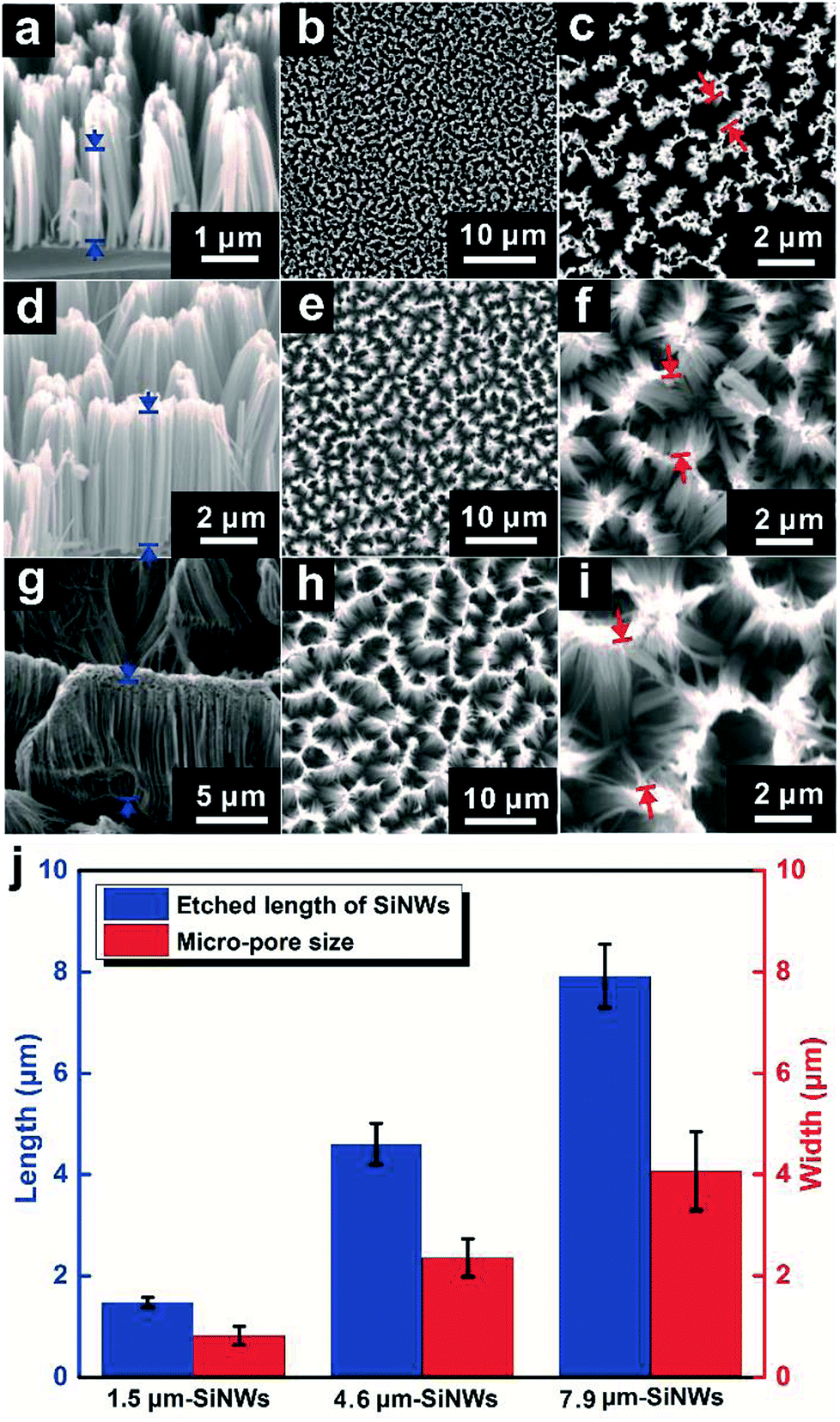 | ||
| Fig. 2 The SEM characterization of SiNW-based electrodes fabricated by electroless etching method with different etching times. (a–c) Side-view and top-view SEM images of the SiNWs surfaces with 10 minutes etching time. The surfaces with (d–f) 20 min and (g–i) 40 min etching time. (j) The measured lengths and pore sizes of the SiNWs as the functions of etching time. The size of micro-scale pores was defined as the width of cavities among the clusters of SiNWs. With etching time increased, the SiNW clusters showed longer lengths (blue bars) and larger pore sizes (red bars). | ||
Electrochemical performances of SiNWs
To study the impact of SiNW structural features on the electrochemical properties of the samples, linear sweep voltammetry performance of different SiNW electrodes was investigated and the results are shown in Fig. 3. For this experiment, all the samples were illuminated with the simulated solar light of 1 kW m−2 and bias potential was applied at the scan rate of 0.1 V s−1. For the production of H2 in the photoelectrocatalytic water splitting reaction using Si-based cathodes, a bias potential is usually needed to initiate the reaction. In Fig. 3a, it is shown that the current densities for all the samples increased with the increase in the applied potential, indicating the promotion of the water splitting reaction at the high applied potential. Within the entire potential range for activating HER (from 0 V to −2.0 V), all the SiNW cathodes showed larger current densities than the flat Si wafer. However, samples with longer lengths showed lower onset potentials, which indicates that the reaction can start at low bias potential. However, the slopes of the curves of current densities as well as their limiting current densities exhibited opposite trends. As the bias voltage linearly increased from 0 V, the sample with the longest etched length, 7.9 μm-SiNWs, first approached to its limiting current density, viz., ∼27 mA cm−2 at −1.1 V. The sample 4.6 μm-SiNWs reached its limiting current density, viz., ∼29 mA cm−2 at −1.5 V with a relative fast acceleration. The sample 1.5 μm-SiNWs was the last to start the reaction, but its current density quickly accelerated and achieved the limiting value of ∼32.5 mA cm−2 at −1.4 V. The photoelectrocatalytic performances of the different SiNW electrodes were related to the nucleation, growth, and release of H2 bubbles, which were greatly affected by the micro/nanostructures formed on the electrodes.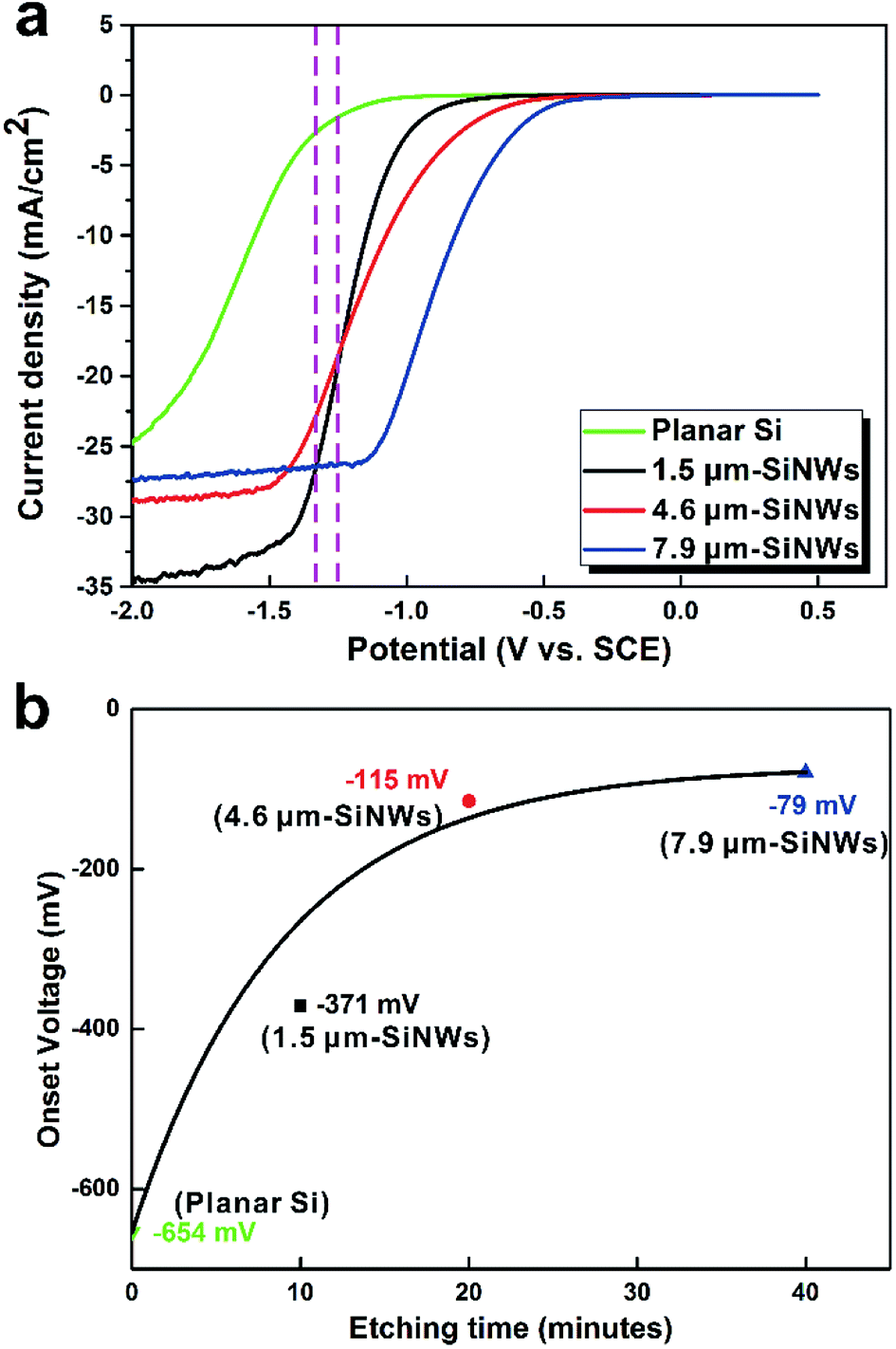 | ||
| Fig. 3 The photoelectrocatalytic properties of various SiNWs surfaces. (a) Photocurrent densities versus applied potentials for different SiNW-based electrodes under simulated one solar illumination. (b) The onset potential measured as a function of the etching time. | ||
As shown in Fig. 3b, when SiNW electrodes were used instead of flat Si electrode, the onset potential decreased, and it decreased further as the length of the SiNW increased. The polynomial fitting shows an exponential decay of onset potential with increase in the length of SiNWs. The effective surface area of SINWs was much larger than that of the flat Si wafer surface; thus, more surface area could be used for the water splitting reaction at the solid–liquid interface, resulting in the decrease in the onset potential values.31 Similar mechanism could be used to explain the decrease in onset potential as the length of the SiNWs increased. Such reduction of onset potential was beneficial for the electrocatalytic reaction.19
In order to exclude the influence of surface chemistry on HER performances of these silicon-based substrates, the samples were further analyzed by XPS (Fig. S3†). The XPS results showed the similar surface chemistry between the flat silicon sample and the SiNWs sample. Therefore, the promotion of electrochemical performance could be mainly attributed to the micro/nanostructure of SiNWs.
Hydrogen bubble formation on electrode surfaces
The behaviour of the H2 bubbles formed on the different sample surfaces was further studied in detail. A high-speed visualization system was used to directly observe H2 bubble formation and release during the photo-induced water splitting process. In general, the bubbles on the planer Si wafer were mostly attached to the surface. After nucleation, they continued to grow, merged together, and were eventually released from the electrode surface. This process of generating hydrogen bubbles on the planar Si surface slowed down gradually. However, the bubbles on the SiNW-based surfaces were much smaller when they left the surface. Fig. 4a–d provide the CCD images of H2 bubbles generated on the planar silicon electrode and on the three SiNW electrode surfaces at the overpotential of −1.5 V vs. SCE (saturated calomel electrode) in 0.5 M H2SO4. We also observed that the H2 bubbles generated on the planar Si surface fully covered the whole electrode surface, while the surfaces of SiNW electrodes quickly released many H2 bubbles of much smaller sizes.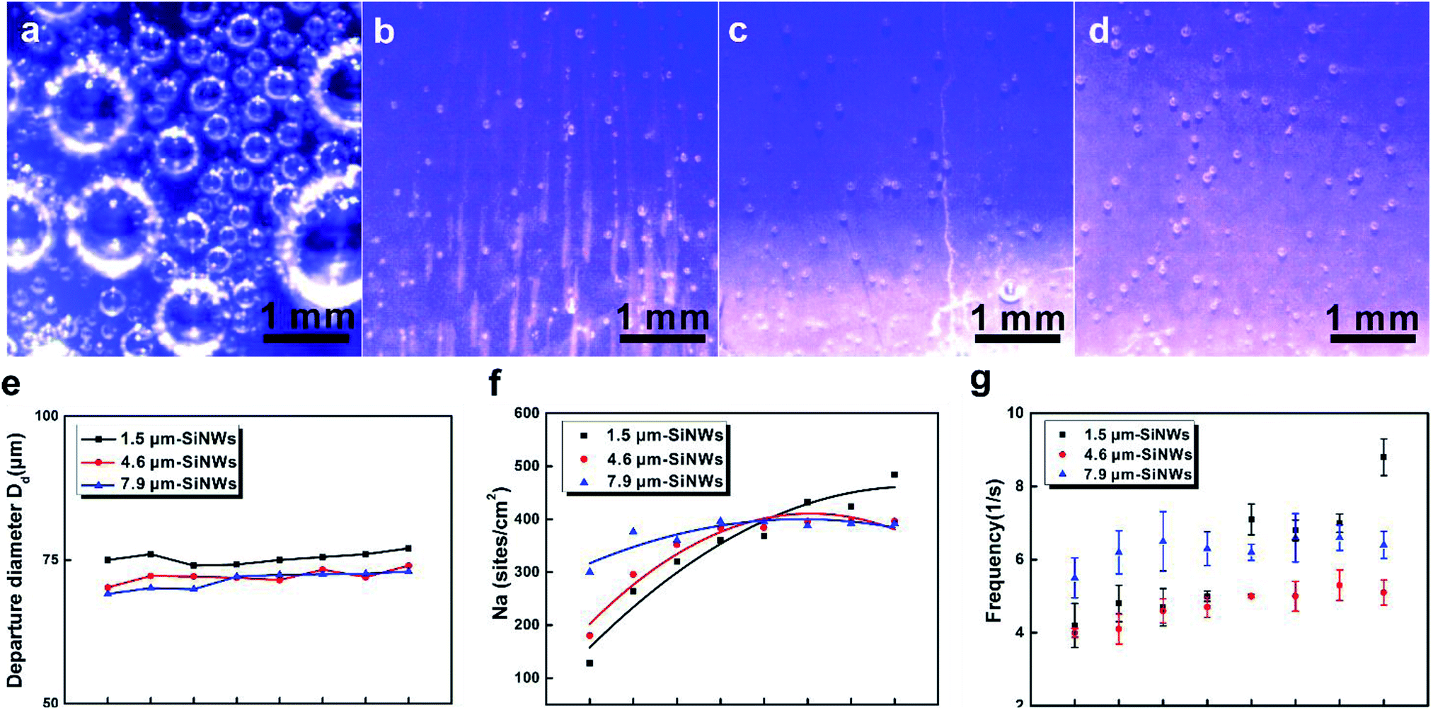 | ||
| Fig. 4 Hydrogen bubble generation on the flat Si surface and SiNWs. The CCD images of H2 bubbles produced on (a) planar silicon electrode, (b) 1.5 μm-SiNWs, (c) 4.6 μm-SiNWs, and (d) 7.9 μm-SiNWs. (e) The average diameters of H2 bubbles departed from nanostructured electrodes at different applied potential. (f) The active nucleation densities on different electrode surfaces at different applied potential. (g) The departure frequency of H2 bubbles from different samples at different applied potential. | ||
The average size of the released H2 bubbles from different SiNWs was plotted in Fig. 4e. It was shown that the bubble release size for all the samples remained almost unchanged as the potential increased. The bubble sizes for 4.6 μm-SiNWs were similar to those for 7.9 μm-SiNWs and smaller than those for 1.5 μm-SiNWs. The bubble size mainly depends on the force balance between the adhesive force and the buoyancy force of the bubbles.16 Larger gas contact angle (indicating smaller water contact angle) in general leads to lower adhesive forces between the bubbles and substrate and also results in smaller size of the released H2 bubbles. Fig. S2† shows the contact angle profiles of various SiNW surfaces: the surface of SiNWs with lengths of 1.5 μm, 4.6 μm, and 7.9 μm had contact angles (CAs) of 30 ± 3°, 16 ± 0.3° and 9 ± 0.1°, respectively, while the flat Si surface had a CA of 36 ± 2°. The hierarchical structures on the nanostructured electrode surfaces comprised nanowire bundles and the micro-pores formed among the nanowire bundles, both of which greatly impacted the surface wettability of the samples.
With the increase in the length of SiNWs, the contact angle decreased. The decrease in CA led to the decrease in the adhesive force and decrease in the sizes of the released H2 bubble. Thus, larger water contact angle of the 1.5 μm-SiNWs could facilitate the growth of H2 bubbles on its surface, which resulted in larger sizes of the released H2 bubbles than those on 4.6 μm-SiNWs and 7.9 μm-SiNWs. Due to the relatively similar contact angles for the 4.6 μm-SiNWs and 7.9 μm-SiNWs, the size of the released bubbles was also relatively similar.
The active nucleation densities of H2 bubbles (Na) and the frequency of bubble release (fd) from the surface were further analyzed for each sample based on the recorded pictures during the photoelectrocatalysis process (Fig. 4f and g). The values for Na were obtained by counting the number of bubbles generated on a unit surface area.
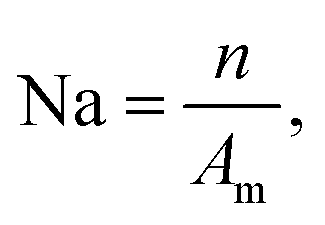 | (1) |
In the photoelectrocatalytic water splitting reaction, the photocurrent was greatly affected by both the diffusion of electrolyte to the electrode surface and the release of the as-formed H2 bubbles from the surface. In general, higher potential can speed up the photoelectrocatalytical reaction to generate more H2 bubbles and produce current with higher density. At the low applied potential regime, the reaction was not very fast and significant amount of H2 was not generated; thus, the electrolyte could access the surface easily. In such a situation, the release of the H2 bubbles from the surface was more critical for the reaction. The stronger adhesion between the shorter SiNWs and the H2 bubbles would result in the low bubble release frequency. Moreover, the effective surface area and the corresponding nucleation density of H2 bubbles on the surface for the shorter SiNW samples were also smaller than those for the longer SiNWs. The lower bubble nucleation density and the lower H2 bubble release frequency account for the smaller current density for shorter SiNW sample, as observed in Fig. 3a in the low potential region. When the applied potential increased, the photoelectrocatalytical reaction became faster and more electrolyte was needed. Thus, the diffusion of the electrolyte to the electrode surface became critical for the reaction in the high potential region. Compared to shorter SiNWs, the longer SiNWs have thicker walls between micropores; hence, they are not favourable for electrolyte diffusion. Thus, the reaction slowed down and lead to the production of less H2 bubbles and decrease in the release frequency for longer SiNW samples at high potential region than those for the shorter SiNW samples. When the H2 bubble release and the electrolyte diffusion reached equilibrium, the photocurrent densities of all the samples reached their limiting values.
Conclusions
This study demonstrated that the electrophotocatalytical performance of the Si-based electrodes was greatly affected by the surface structures. The nanostructured SiNW electrodes were more effective than flat Si electrode for the photoelectrocatalytical water splitting reaction. The nanostructures on the surface provided more effective surface area for the nucleation of H2 bubbles. The increased water wettability of the SiNW electrodes also helped the decrease in the adhesion of the as formed H2 bubbles on the surface and facilitated their release. Moreover, the SiNW electrodes showed structure-dependent photoelectrocatalytical properties. The longer SiNW samples presented better performance in the low potential region, while the shorter SiNW samples were more efficient in the high potential region. Thus, this study provided additional insights into the impact of the micro/nanostructures on H2 evolution during the photoelectrocatalytic water splitting process.Conflicts of interest
There are no conflicts to declare.Acknowledgements
We are grateful to the financial support from National Key R&D Program of China (2016YFB0402100), National Natural Science Foundation of China (Grant No: 51521004, 51420105009, 51403127, 21401129), the 111 Project (Grant No. B16032) The authors also thank Instrumental Analysis Center of Shanghai Jiao Tong University for access to SEM.References
- Y. W. Chen, J. D. Prange, S. Duhnen, Y. Park, M. Gunji, C. E. D. Chidsey and P. C. McIntyre, Nat. Mater., 2011, 10, 539–544 CrossRef CAS PubMed.
- W. Cui, Z. H. Xia, S. Wu, F. J. Chen, Y. G. Li and B. Q. Sun, ACS Appl. Mater. Interfaces, 2015, 7, 25601–25607 CrossRef CAS PubMed.
- S. E. Hosseini and M. A. Wahid, Renewable Sustainable Energy Rev., 2016, 57, 850–866 CrossRef CAS.
- S. F. Huang, H. F. Zhang, Z. L. Wu, D. Z. Kong, D. D. Lin, Y. L. Fan, X. J. Yang, Z. Y. Zhong, S. H. Huang, Z. M. Jiang and C. W. Cheng, ACS Appl. Mater. Interfaces, 2014, 6, 12111–12118 CrossRef CAS.
- T. W. Kim, Y. Ping, G. A. Galli and K. S. Choi, Nat. Commun., 2015, 6, 8769 CrossRef CAS.
- D. Larcher and J. M. Tarascon, Nat. Chem., 2015, 7, 19–29 CrossRef CAS.
- N. S. Lewis, Science, 2016, 351, aad1920 CrossRef PubMed.
- S. J. A. Moniz, S. A. Shevlin, D. J. Martin, Z. X. Guo and J. W. Tang, Energy Environ. Sci., 2015, 8, 731–759 RSC.
- M. Z. Rahman, C. W. Kwong, K. Davey and S. Z. Qiao, Energy Environ. Sci., 2016, 9, 709–728 RSC.
- R. S. Sprick, B. Bonillo, R. Clowes, P. Guiglion, N. J. Brownbill, B. J. Slater, F. Blanc, M. A. Zwijnenburg, D. J. Adams and A. I. Cooper, Angew. Chem., Int. Ed., 2016, 55, 1824–1828 CrossRef PubMed.
- F. Yilmaz, M. T. Balta and R. Selbas, Renewable Sustainable Energy Rev., 2016, 56, 171–178 CrossRef CAS.
- Z. Yu, F. Li and L. C. Sun, Energy Environ. Sci., 2015, 8, 760–775 RSC.
- M. S. Faber, R. Dziedzic, M. A. Lukowski, N. S. Kaiser, Q. Ding and S. Jin, J. Am. Chem. Soc., 2014, 136, 10053–10061 CrossRef CAS PubMed.
- T. Jiang, Z. G. Guo and W. M. Liu, J. Mater. Chem. A, 2015, 3, 1811–1827 RSC.
- Z. Y. Lu, Y. J. Li, X. D. Lei, J. F. Liu and X. M. Sun, Mater. Horiz., 2015, 2, 294–298 RSC.
- P. C. Zhang, S. S. Wang, S. T. Wang and L. Jiang, Small, 2015, 11, 1939–1946 CrossRef CAS PubMed.
- J. Y. Long, L. Pang, P. X. Fan, D. W. Gong, D. F. Jiang, H. J. Zhang, L. Li and M. L. Zhong, Langmuir, 2016, 32, 1065–1072 CrossRef CAS PubMed.
- Y. J. Li, H. C. Zhang, T. H. Xu, Z. Y. Lu, X. C. Wu, P. B. Wan, X. M. Sun and L. Jiang, Adv. Funct. Mater., 2015, 25, 1737–1744 CrossRef CAS.
- Z. Y. Lu, W. Zhu, X. Y. Yu, H. C. Zhang, Y. J. Li, X. M. Sun, X. W. Wang, H. Wang, J. M. Wang, J. Luo, X. D. Lei and L. Jiang, Adv. Mater., 2014, 26, 2683–2687 CrossRef CAS PubMed.
- I. Oh, J. Kye and S. Hwang, Nano Lett., 2012, 12, 298–302 CrossRef CAS PubMed.
- U. Sim, H. Y. Jeong, T. Y. Yang and K. T. Nam, J. Mater. Chem. A, 2013, 1, 5414–5422 RSC.
- L. Shen, C. L. He, J. Qiu, S. M. Lee, A. Kalita, S. B. Cronin, M. P. Stoykovich and J. Yoon, ACS Appl. Mater. Interfaces, 2015, 7, 26043–26049 CrossRef CAS PubMed.
- S. Chandrasekaran, T. Nann and N. H. Voelcker, Nano Energy, 2015, 17, 308–322 CrossRef CAS.
- M. H. Lee, K. Takei, J. J. Zhang, R. Kapadia, M. Zheng, Y. Z. Chen, J. Nah, T. S. Matthews, Y. L. Chueh, J. W. Ager and A. Javey, Angew. Chem., Int. Ed., 2012, 51, 10760–10764 CrossRef CAS PubMed.
- L. N. Dong, X. J. Quan and P. Cheng, Int. J. Heat Mass Transfer, 2014, 71, 189–196 CrossRef.
- B. S. Kim, S. Shin, S. J. Shin, K. M. Kim and H. H. Cho, Langmuir, 2011, 27, 10148–10156 CrossRef CAS PubMed.
- Z. P. Huang, H. Fang and J. Zhu, Adv. Mater., 2007, 19, 744–748 CrossRef CAS.
- Z. P. Huang, N. Geyer, P. Werner, J. de Boor and U. Gosele, Adv. Mater., 2011, 23, 285–308 CrossRef CAS PubMed.
- S. W. Chang, V. P. Chuang, S. T. Boles, C. A. Ross and C. V. Thompson, Adv. Funct. Mater., 2009, 19, 2495–2500 CrossRef CAS.
- R. Chen, M. C. Lu, V. Srinivasan, Z. Wang, H. H. Cho and A. Majumdar, Nano Lett., 2009, 9, 548–553 CrossRef CAS PubMed.
- J. H. Oh, T. G. Deutsch, H. C. Yuan and H. M. Branz, Energy Environ. Sci., 2011, 4, 1690–1694 RSC.
Footnotes |
| † Electronic supplementary information (ESI) available: Experimental section and supplementary figures. See DOI: 10.1039/c8ra07905f |
| ‡ These authors contribute equally to this work. |
| This journal is © The Royal Society of Chemistry 2018 |