
 Open Access Article
 This Open Access Article is licensed under a
 Creative Commons Attribution 3.0 Unported Licence
Potential solution-induced HfAlO dielectrics and their applications in low-voltage-operating transistors and high-gain inverters†
Gang He *ab,
Wendong Lia,
Zhaoqi Suna,
Miao Zhanga and
Xiaoshuang Chenc
*ab,
Wendong Lia,
Zhaoqi Suna,
Miao Zhanga and
Xiaoshuang Chenc
aSchool of Physics and Materials Science, Radiation Detection Materials & Devices Lab, Anhui University, Hefei 230601, P. R. China. E-mail: hegang@ahu.edu.cn
bInstitute of Physical Science and Information Technology, Anhui University, Hefei 230601, P. R. China
cNational Laboratory for Infrared Physics, Chinese Academy of Sciences, Shanghai Institute of Technical Physics, 500 Yutian Road, Shanghai 200083, P. R. China
First published on 30th October 2018
Abstract
Recently, much attention has been paid to the investigation of solution-driven oxides for application in thin film transistors (TFTs). In current study, a fully solution-based method, using 2-methoxyethanol as solvent, has been adopted to prepare InZnO thin films and HfAlOx gate dielectrics. Amorphous HfAlOx thin films annealed at 600 °C have shown a high transparency (>85%), low leakage current density (6.9 × 10⁻⁹ A cm−2 at 2 MV cm−1), and smooth surface. To verify the potential applications of HfAlOx gate dielectrics in oxide-based TFTs, fully solution-induced InZnO/HfAlOx TFTs have been integrated. Excellent electrical performance for InZnO/HfAlOx TFTs annealed at 450 °C has been observed, including a low operating voltage of 3 V, a saturated mobility of 5.17 cm2 V−1 s−1, a high Ion/Ioff of ∼106, a small subthreshold swing of 87 mV per decade, and a threshold voltage shift of 0.52 V under positive bias stress (PBS) for 7200 s, respectively. In addition, time dependent threshold voltage shift under PBS could be described by a stretched-exponential model, which can be due to charge trapping in the semiconductor/dielectric interface. Finally, to explore the possible application in logic operation, a resistor-loaded inverter based on InZnO/HfAlOx TFTs has been built and excellent swing characteristic and well dynamic behavior have been obtained. Therefore, it can be concluded that fully solution-driven InZnO/HfAlOx TFTs have demonstrated potential application in nontoxic, eco-friendly and low-power consumption oxide-based flexible electronics.
1 Introduction
Large-area backplane electronics for upcoming displays have attracted more attention and demonstrated potential applications in next-generation active matrix displays and flexible electronics, such as smart windows, transparent tablets, interactive white boards, and so on.1,2 To operate these frontier displays, transparent thin-film transistors (TFTs) with high performance should be built as switching or driving components. Currently, amorphous metal-oxide TFTs have obtained increasing interest owing to the high electron mobility, high transparency, excellent electrical performance for high-speed driving, and solution processability for advanced processing, which is superior to those of the conventional amorphous or poly silicon TFTs.3–5 Among the various oxide semiconductor materials, indium–zinc oxide (IZO)-based oxide semiconductor has been considered a promising candidate for the active layer of oxide-based TFTs, exhibiting an optical transmittance of more than 85%, an optical band gap of around 3.5 eV, and high mobility.6–9 However, the high power consumption attributed to the high operating voltage impedes the application of oxide-based TFTs.10–12 To realize the potential application of oxide-based TFTs in mobile and portable devices, high-k gate dielectrics have been selected to enhance the capacitive coupling and reduce the power consumption.Much effort has been dedicated to the investigation of binary high-k dielectric materials, such as ZrO2, TiO2, and HfO2 in the oxide-based TFTs due to their high dielectric constant and wide band gap.13–15 Considering their desirable electrical properties and good process compatibility with oxide semiconductors, Hf-based oxide dielectrics have been regarded as good candidates in the display industry.5,16 However, the low crystallization temperature and the formation of the grain boundaries for Hf-based high-k gate dielectrics contribute to the electrical leakage paths and the increased gate leakage current.17,18 The grain boundary of the crystalline structures in the gate insulator, which degrades the electrical performance, is a critical issue. To resolve this issue, amorphous high-k dielectrics have been developed as the potential candidates for the optimal operation of the gate insulator in TFTs.
To increase the crystallization temperature, additional dopants, for instance, Si, Ti, and La are introduced into HfO2 to form amorphous Hf-based high-k oxides.19–21 Consequently, the crystalline phase of the Hf-based gate dielectrics were suppressed up to 900 °C.22 However, the oxygen diffusion and the reduced dielectric constant after doping degrade the device's performance and prevent its application in TFTs devices. Fortunately, Al incorporating into HfO2 worked effectively with increased crystallization temperature and suppressed oxygen diffusion.23,24 Furthermore, Al-doped Hf-based oxide showed a considerably low leakage current due to its larger band gap and suitable conduction band offset.25 However, the use of vacuum-based deposition method to obtain Al-doped Hf-based gate oxides, such as atomic layer deposition26 (ALD) and chemical vapour deposition27 (CVD), are limited and incompatible with large-scale production and low cost fabrication. Fortunately, solution-based methods such as inkjet printing, dip-coating, and spin-coating are appropriate for resolving this issue. Operational solution-processed oxide TFTs represent a vital part of this vision, and the stringent requirements on film quality and electrical characteristics make the realization of such TFTs a challenging goal and a key development milestone.28–30
In current work, we introduce a simple fabrication process with a large area and low-cost processability for a solution-processed amorphous hafnium–aluminum oxide (HfAlOx) gate insulator. The correlation between microstructure and dielectric properties of promising amorphous high-k HfAlOx films has been investigated. The surface morphology and leakage current behaviors of solution processed HfAlOx thin films as a function of annealing temperature were examined in terms of its application as gate insulators. To verify the possibility of the solution-derived amorphous HfAlOx thin film as gate dielectric in CMOS logics, all-solution-processed IZO-based TFTs and resistor-loaded inverters were also fabricated and examined systematically. Therefore, it can be concluded that the optimized IZO/HfAlOx TFTs exhibited optimized electrical performance under a low operating voltage of 3 V, including a high Ion/Ioff of around 6.01 × 10⁷, and a high μsat of 5.17 cm2 V−1 S−1. Meanwhile, the resistor-loaded inverter based on IZO/HfAlOx TFT demonstrates full swing characteristics with a gain of 4.32 at 4.0 V.
2 Experimental
2.1 Precursor solution preparation and characterization
The InZnO precursor solution was prepared by dissolving In(NO3)3·xH2O and Zn(NO3)3·6H2O in 2-methoxyethanol. The concentration of IZO precursor solution is 0.1 M and the ratio of In![[thin space (1/6-em)]](https://www.rsc.org/images/entities/char_2009.gif) :Zn is 1:1. The HfAlO precursor solution was prepared by dissolving HfCl4 and Al(NO3)3·9H2O in 2-methoxyethanol. The purity of all the starting materials is 99.9% and purchased from Aladdin pharmaceuticals. The concentration of HfAlO precursor solution is 0.1 M and the ratio of Hf:Al is 2:1. All precursor solutions were stirred vigorously in 600 rpm for 6 h at room temperature. The thermal behaviors of InZnO and HfAlO xerogel were measured using a thermal-gravimetric analyzer (TGA) with a heating rate of 10 °C min−1 (STA449F3) in air.
:Zn is 1:1. The HfAlO precursor solution was prepared by dissolving HfCl4 and Al(NO3)3·9H2O in 2-methoxyethanol. The purity of all the starting materials is 99.9% and purchased from Aladdin pharmaceuticals. The concentration of HfAlO precursor solution is 0.1 M and the ratio of Hf:Al is 2:1. All precursor solutions were stirred vigorously in 600 rpm for 6 h at room temperature. The thermal behaviors of InZnO and HfAlO xerogel were measured using a thermal-gravimetric analyzer (TGA) with a heating rate of 10 °C min−1 (STA449F3) in air.
2.2 Thin film fabrication and characterization
The substrate was heavily doped p-Si (0.0015 Ω cm) and acted as gate electrode. The substrates were ultrasonic cleaned in acetone, alcohol and deionized water in sequence for 10 min. The substrates were treated by oxygen plasma for 10 min to enhance hydrophilicity before deposition. The HfAlO solution was filtered through a 0.22 μm syringe filter and spun on the substrates at 5000 rpm for 20 s. Then the films were baked at 150 °C for 10 min and repeat previous procedure once. After deposition, the samples were treated by ultraviolet (UV) light for 30 min and annealed at 300, 400, 500 and 600 °C for 1 h in air. The power of UV lamp was 1 kW and the UV lamp was 20 cm from the samples. The microstructures of HfAlOx thin films were investigated by X-ray diffractometer (XRD, MXP 18AHFMAC Science, Yokohama). The absorbance and transmittance of HfAlOx films deposited on quartz substrate were measured by a UV-Vis spectrophotometer (Shimadzu, UV-2550). The surface morphologies of HfAlO were measured by using atomic force microscope (AFM, Smart Lab, Multimode 8). The chemical compositions of HfAlOx were analyzed by X-ray photoelectron spectroscopy (XPS, ESCALAB 250Xi). C 1s peak at 284.6 eV was taken as a reference for charge correction. The charge neutralizations of X-ray bombarded samples were performed by flood guns and spectral deconvolution was performed by Shirley background subtraction using a Voigt function convoluting Gaussian and Lorentzian functions. The thicknesses of HfAlOx and IZO thin films were measured by spectroscopic ellipsometry (SE, SANCO Co, Shanghai, SC630). A MOS structure of Al/HfAlO/p+-Si was used to measure the dielectric properties of HfAlO films by an impedance analyzer (Agilent 4294A).2.3 TFTs fabrication and characterization
The InZnO solution was spun on the HfAlOx films at 5000 rpm for 20 s. Then the samples were annealed at 350, 400, 450 and 500 °C for 1 h in air. Finally, the Al source and drain electrodes were deposited on the films via a shadow mask. The channel length and width were 100 and 1000 μm. In addition, the SiO2-based TFTs were preparation for comparison. The 200 nm-thick SiO2 was obtained by heavily doped p-Si with the thermal oxidation procedure. The detailed schematic diagram of the solution-derived IZO and HfAlOx thin films and In2O3-based TFTs fabrication are demonstrated in Fig. S1 (ESI).† The electrical properties of the integrated TFTs were measured by using semiconductor parameter analyzers (Keithley 2636B; Agilent B1500A) in a dark box. The saturation mobility (μsat) was extracted from transfer characteristics using the following equation31where Ci is the areal capacitance of the gate dielectric, W and L are the channel width and length of the TFT, VG is the gate voltage and VTH is the threshold voltage, which was determined in the saturation region by linear fitting ID1/2 vs. VG plot. The density of interface states (Dit) can be inferred using the following equation,31

where k, T, and q are Boltzman's constant, absolute temperature, and charge quality, respectively.
3 Results and discussion
3.1 Microstructure analysis and surface morphology of solution-derived HfAlOx thin films
To investigate the thermal behavior of IZO and HfAlOx thin films, TGA measurement of HfAlOx and IZO precursor solutions was performed with a heating rate of 10 °C min−1 and the experimental result is demonstrated in Fig. 1. For IZO xerogel, the initial decrease of weight for IZO below 180 °C is attributed to the decomposition of the residual nitrate species originating from the metal nitrate salt.32 The continuous decreased weight between 180 °C to 350 °C can is mainly due to the dihydroxylation.33 When the temperature exceeds 350 °C, the reduction in mass has not been observed, suggesting that complete transformation from xerogel to IZO oxide has been completed. For HfAlOx xerogel, the transformation in the decomposition process of HfAlOx xerogel is not similar to IZO xerogel. It could be noted that the dehydroxylation and alloy reaction begin at the initial stage. A more pronounced, gradual mass loss over several hundred degrees have been detected. Conversion of the HfAlO precursor to the corresponding oxide is completed by 600 °C. Based on this dehydroxylation behavior, the annealing temperature range for clear gate switching modulation of successful oxide TFTs is estimated to range from 350 °C to 600 °C. | ||
| Fig. 1 Thermal behavior of the solution-induced IZO and HfAlOx xerogel. | ||
The evolution of the microstructure of the spin-coated HfAlOx films annealed at various temperatures was investigated by XRD measurements and the results are demonstrated in Fig. 2. No apparent diffraction peaks of crystalline phase in XRD patterns have been observed in the films regardless of the annealing temperature, indicating that the HfAlOx films are identified as amorphous phase. It is confirmed further that introducing appropriate amount of Al2O3 in HfO2 would remarkably block the crystallization of the HfO2 films and lead to the increase of crystallization temperature of HfO2, which is in good agreement with our previous investigation.34 Being a dielectric layer for the bottom-gated TFTs, the amorphous phase is more suitable than the crystalline phase owing to its smooth surface, low leakage current, and high breakdown electric field. According to the grain-boundary charge-trapping model,35 the grain boundary usually acts as the trapping and scattering center in polycrystalline film, leading to the high leakage current and the degraded insulating reliability.33 Such dielectrics certainly show high off-state current in TFT devices. In addition, the amorphous thin films generally exhibit smoother surface roughness compared with the crystalline ones, which is a prerequisite for expeditious charge carrier mobility in the TFT devices.36
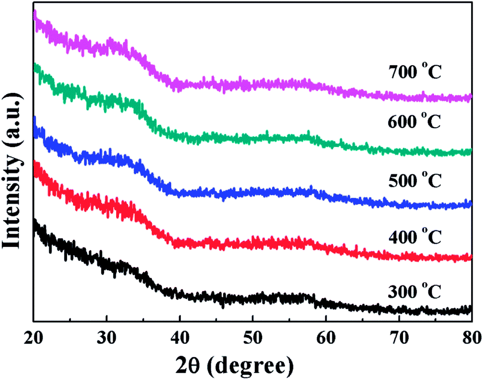 | ||
| Fig. 2 Annealing temperature dependent XRD patterns of HfAlOx films. | ||
It is well known that high-performance TFTs should have dielectric layers with smooth surface as the carrier transport is affected by the interface between the channel and the dielectric layers. To investigate the evolution of the surface morphology of HfAlOx films as a function of annealing temperature, AFM images of the solution-derived HfAlOx films are shown in Fig. 3. The root-mean-square (RMS) values of HfAlO films annealed at 300, 400, 500 and 600 °C are 0.266, 0.189, 0.205, and 0.147 nm, respectively. It is obvious to see that RMS values smaller than 1 nm are observed for solution-processed HfAlOx dielectrics, which is conductive to the growth of high-quality channel layer and improve the TFTs' performance. The smooth surface of the HfAlO films is not only attributed to their amorphous structure, but also to the use of UV annealing treatment. Based on the investigation from Tak et al., it can be noted that UV treatment consists of three main reactions (Fig. S2†). First, physical bonds are effectively converted into chemical bonds. It is proposed that the energy provided by UV light is sufficient to decompose residual weak chemical bonds in spin-coated oxide films, and the simultaneous thermal treatment induces the reorganization and rearrangement of the decomposed chemical bonds into strong chemical bonds. Second, UV treatment promoted the oxidation of the gate dielectric films and led to a lower number of uncoordinated oxygen species. Third, the increased surface energy of the oxide films indicates highly chemically reactive states and improved surface smooth. Therefore, it can be concluded that UV treatment can effectively accelerate the decomposition of organic ligands, reduce the nanopores in the films, and attribute the increased surface energy and the decreased surface roughness.17,37,38
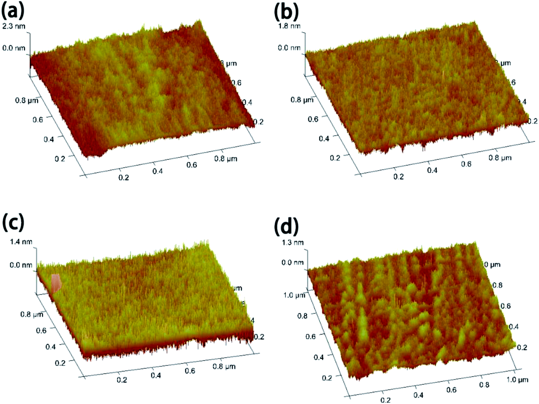 | ||
| Fig. 3 Surface morphologies of (a) 300 °C, (b) 400 °C, (c) 500 °C and (d) 600 °C-annealed HfAlOx films. | ||
3.2 Optical properties analysis of solution-derived HfAlOx thin films
To investigate the optical properties of the HfAlOx films, transmittance and absorbance of the HfAlOx films were measured. Fig. 4 shows the optical transmittance and absorbance spectra of HfAlOx films as a function of annealing temperature. All the samples demonstrate high average optical transmittance values (>85%) in the visible region, indicating that HfAlOx films can be considered as candidate dielectric materials for transparent devices. By using a standard Tauc plot method, the optical bandgap (Eg) is calculated and the results are displayed in Fig. 4b. It can be seen that the Eg value increases from 4.76 to 5.57 eV when annealing temperature changes from 300 to 600 °C. Apparently, blue shift in band gap has been detected with the increase of the annealing temperature. For the low-temperature-driven HfAlOx thin film, the presence of defects in the thin film would produce localized states in the bandgap, leading to the reduced bandgap energy of the film. After high temperature annealing, the annihilation of oxygen vacancies/defects results in a decrease of the density of states in the band structure, which leads to an increased bandgap energy of the HfAlOx thin films.28 The increased Eg is beneficial for suppressing the carrier transport from channel to gate dielectric. | ||
| Fig. 4 (a) Optical transmittance and (b) band gap of HfAlOx films annealed at different temperature. | ||
3.3 Chemical bonding states of HfAlOx thin films
The chemical bonding states and compositions of sputtering-derived HfAlOx thin films were analyzed by XPS. Fig. S3† displays the survey spectra of the HfAlOx thin films as a function of annealing temperature. It can be noted that Hf, Al, O, and C have been detected, suggesting that all the films are free from other contaminations and Al is successfully incorporated into the HfO2 gate dielectrics. O 1s XPS spectra for HfAlOx thin films have been demonstrated in Fig. 5a and deconvoluted O 1s spectra centered at 530.14 eV, 531.36 eV and 532.73 eV, have been observed, respectively. The peak located at 530.14 eV is assigned to the metal–oxygen bond (OI) in HfAlOx lattice and the peak located at 531.36 eV is attributed to the oxygen vacancy (OII) in lattice.39,40 The peak centered at 532.73 eV may be related to loosely bound oxygen on the surface of films, such as adsorbed H2O and –OH.41 Increasing the annealing temperature from 300 to 600 °C, the fraction of OI in HfAlOx increases and OII and OIII species decrease, which indicates that high temperature annealing reduces the oxygen vacancy and hydroxyl species, and improves the metal–oxygen lattice. The presence OII and OIII generally creates trap and defect states in the band gap of the dielectric film, leading to the increased leakage current and the reduced breakdown voltage.42 Therefore, higher temperature annealing is effective in controlling the oxygen vacancy and bonded oxygen content and obtain high quality high-k gate dielectric for application in TFT devices. To obtain more information on chemical bonding states from HfAlOx thin films, the evolution of the Hf 4f and Al 2p core-level XPS spectra related to annealing temperature has been investigated, as shown in Fig. 5b and c. Compared to HfO2, the doublet peaks corresponding to Hf 4f5/2 and Hf 4f7/2 for HfAlOx thin films shift towards higher binding energy sides, indicating the formation of Hf-aluminate.34 However, for the 600 °C-annealed sample, the shift of binding energy in Hf 4f peak towards lower energy side has been detected, which can be due to the decomposition of HfAlOx and partial formation of HfO2. The same trend has been observed for Al 2p core-level XPS spectra. | ||
| Fig. 5 XPS spectra of O 1s (a), Hf 4f (b), and Al 2p (c) peaks for HfAlOx dielectrics as a function of annealing temperature. | ||
3.4 Dielectric and electrical properties of solution-derived HfAlOx thin films
To investigate the annealing temperature dependence on the dielectric and electrical properties of the solution-driven HfAlOx thin films, MOS capacitors based on Al/HfAlO/p+-Si were constructed. Fig. 6a shows the areal capacitance (C) as a function of frequency (f) for HfAlOx capacitors. The areal capacitance of HfAlO capacitors annealed at 300, 400, 500 and 600 °C is 475, 404, 355, and 326 nF cm−2 at 20 Hz, respectively. It can be noted that reduction in the areal capacitance has been observed with the annealing temperature increasing from 300 to 600 °C. Generally speaking, water molecules can be absorbed by polarizable hydroxyl groups. Previous XPS results have confirmed the existence of the large number of polarizable hydroxyl groups in low-temperature-processed HfAlOx thin films. Therefore, absorbed water molecules would lead to the high capacitance owing to the high dielectric constant of water molecules.43 At the same time, the slight decreases for the areal capacitance in the high frequency range can be attributed to the limited polarization response time.44 To evaluate the leakage behavior of the HfAlOx thin films, the corresponding leakage current densities and electric field characteristics of MOS capacitors annealed at different temperatures have been shown in Fig. 6b. For the low-temperature-annealing sample, the relatively large leakage current density may be attributed to the incomplete decomposition of hydroxyl groups. The reduced leakage current density has been observed with the increase in the annealing temperature, which probably originates from the gradually decomposition of residuals and the reduced defect density. For the 600 °C-annealed sample, the lowest leakage current density of 6.0 × 10⁻⁹ A cm−2 at 2 MV cm−1 has been achieved. As a result, it can be inferred that the excellent electrical performance for 600 °C-annealed solution-processed HfAlOx dielectric thin films guarantees its potential application in low-voltage transistor. | ||
| Fig. 6 (a) Capacitance–frequency curves and (b) leakage current density–electric field curves of Al/HfAlO/p+-Si capacitor. | ||
3.5 Solution-driven IZO TFTs based on HfAlOx dielectric
Based on above analysis, it can be noted that the 600 °C-processed HfAlOx gate dielectric completely meets the application requirements of TFTs. Before investigating the feasibility of solution-processed HfAlOx as gate dielectric in TFTs, the possibility of solution-derived IZO/SiO2 TFTs with bottom-gate and top-contact architecture was evaluated. The solution-processed IZO channel layers were annealed at 350–500 °C. The output curves of each IZO/SiO2 TFTs are shown in Fig. S4† and the annealing temperature dependent output characteristics of the IZO/SiO2 TFTs, at a gate voltage of (VGS) of 40 V, are depicted in Fig. 7a. The low saturation current at 350 °C may mainly attributed to the existed hydroxyl groups and the formation of defect states. When increasing the annealing temperature, the increased saturation current has been observed, indicating the reduced lattice defects, such as hydroxides and residual impurities.45 The representative transfer characteristics of In2O3 TFTs, at a drain voltage of (VDS) of 20 V, are displayed in Fig. 7b. The μsat and threshold voltage (VTH) in the saturation region were determined from linear fits to the dependence of the square root of ID on VG. The subthreshold swing (SS) was extracted from the linear portion of a plot of the logID versus VG. The extracted key TFTs performance parameters as a function of annealing temperature are summarized in Table 1. It can be seen that μsat values increase from 0.15 to 3.08 cm2 V−1 S−1 with the increase in annealing temperature, which can be due to the decomposition of organic groups and the formation of metal–oxygen bonds. Meanwhile, increase in Ion/Ioff and reduction in SS have been detected with the increased annealing temperature, which can be attributed to the reduced oxygen vacancy and free carrier concentration. However, further increasing the annealing temperature for IZO channel layer to 500 °C results in the degraded device performance, originating from the increased trap states near the IZO/SiO2 interface, confirmed by the Dit values shown in Table 1. On the basis of the extracted electrical parameters, it can be noted that the solution-derived 450 °C-annealed IZO/SiO2 TFTs demonstrates the optimized electrical performance, including a high μsat of 1.41 cm2 V−1 S−1, a high Ion/Ioff value of 106, and a small SS value of 0.507 V dec−1, respectively. However, all the TFTs devices operate at high voltages and hence increase the power consumption due to the low dielectric constant for SiO2. To decrease the operation voltage and reduce the power consumption of solution-derived IZO TFTs, high-k gate dielectric should be explored.
 | ||
| Fig. 7 (a) Output and (b) transfer curves of IZO/SiO2 TFTs as a function of annealing temperature. | ||
| VTH (V) | ΔVTH (V) | Ion/Ioff | μ (cm−2 V−1 s−1) | SS (mV per decade) | NT (cm−2) | |
|---|---|---|---|---|---|---|
| 350 °C | 13.5 | 2.5 | 4 × 10⁶ | 0.15 | 633 | 9.57 × 10¹¹ |
| 400 °C | 15.0 | 3.2 | 4 × 10⁶ | 0.40 | 646 | 9.78 × 10¹¹ |
| 450 °C | 13.9 | 2.2 | 8 × 10⁶ | 1.42 | 507 | 7.46 × 10¹¹ |
| 500 °C | 13.0 | 2.6 | 4 × 10⁴ | 3.08 | 2469 | 4.02 × 10¹² |
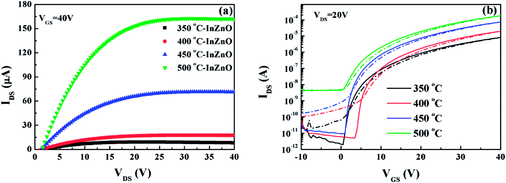
In order to validate the usefulness of high-k HfAlOx film as gate insulators for TFTs, bottom-gated fully solution-derived IZO/HfAlOx TFTs were fabricated. Previous 600 °C-annealed HfAlOx has been adopted to act as the dielectric layer due to its relatively low leakage current and good dielectric properties. A solution-processable IZO precursor solution was spin-coated on a HfAlOx/Si stack, followed by annealing from 350 to 500 °C to pursue the optimized TFTs device performance.
Fig. S5† displays the output curves of each TFT and the summarized output curves of IZO/HfAlOx TFTs at a VGS of 3 V are shown in Fig. 8a. It can be seen that the output characteristics of IZO/HfAlOx TFTs exhibit typical n-channel conduction behavior with clear pinch-off voltage and current saturation. By comparing the transfer curves of IZO/HfAlOx TFTs with IZO/SiO2 TFTs, it can be seen that the off-current region increases with decreasing VGS for the IZO/HfAlOx TFTs while the IZO/SiO2 TFTs remains flat, which can be due to the smaller band gap of HfAlOx compared with SiO2, and thus, the carrier injection into the HfAlOx will be much easier than into SiO2. Interestingly, by replacing SiO2 with high-k HfAlOx thin film, the operation voltage drastically reduces from 40 V to 3 V. As a result, the HfAlOx/IZO TFTs expend lower consumption than the SiO2/IZO TFTs. Because the field-induced current is proportional to the field-induced charge density, a reasonable technique to achieve low-voltage operation in TFT is to use HfAlOx as the gate dielectric, which can afford greater surface charge density at the semiconductor/dielectric interface. Fig. 8b shows the representative transfer characteristics of TFTs based on 600 °C-annealed HfAlOx films as a function of the annealing temperature. The extracted electrical characteristics, including the μsat, Ion/Ioff, VTH, Dit, and SS, of HfAlOx/IZO TFTs with different annealing temperatures were summarized in Table 2. With the increase of the annealing temperature from 350 to 450 °C, VTH and SS decrease from 1.63 and 120 to 1.14 V and 87 mV dec−1, while Ion/Ioff and μsat increase from 104 and 0.80 to 106 and 9.50 cm2 V−1 S−1, respectively. Apparently, the optimized electrical performance has been achieved for 450 °C-annealed HfAlOx/IZO TFTs.
 | ||
| Fig. 8 (a) Output and (b) transfer curves of IZO/HfAlO TFTs as a function of annealing temperature. | ||
| VTH (V) | ΔVTH (V) | Ion/Ioff | μ (cm−2 V−1 s−1) | SS (mV per decade) | NT (cm−2) | |
|---|---|---|---|---|---|---|
| 350 °C | 1.63 | 0.06 | ∼104 | 0.80 | 120 | 1.98 × 10¹² |
| 400 °C | 1.23 | 0.10 | ∼104 | 2.52 | 177 | 3.86 × 10¹² |
| 450 °C | 1.14 | 0.19 | ∼106 | 5.17 | 87 | 8.93 × 10¹¹ |
| 500 °C | 1.16 | 0.09 | ∼105 | 9.50 | 183 | 4.06 × 10¹² |
In the solution-derived channel layer thin films, oxygen vacancies form when dehydroxylation and polycondensation occur. Thus, it is expected that annealing at a higher temperature leads to the reduction of oxygen vacancy and the formation of more metal–oxygen bonds. As a result, VTH shifts towards negative direction as the annealing temperature increases due to the reduced interfacial defects acting as the carrier trap at IZO/HfAlOx interface. With increasing the annealing temperature, the oxygen vacancy and free carrier concentration decrease. As a result, Ion/Ioff initially increases because of the reduced Ioff. As we know, a small SS is expected to achieve a high operation speed and low power consumption. Normally, the SS value is dependent on the traps located in channel/dielectric interface.37 With the increase in annealing temperature, the reduction in SS value may be attributed to the large areal capacitance of the HfAlOx dielectric layer and the electronic-clean interface between IZO and HfAlOx. Based on Jeong's report,46 it can be observed that the conduction band minimum in the metal oxide semiconductors is primarily composed of dispersed vacant s states with short interaction distances for efficient carrier transportation, which can be achieved in ionic oxide but not obviously in hydroxide. Therefore, higher temperature annealing accelerates the decomposition of –OH groups and the alloy reaction and leads to the formation of metal–oxygen framework, which contributes fewer defects in both bulk and interface. For the top-gated TFTs, the carrier transport is limited in a narrow region at channel/dielectric interface. In this regard, the reduced defects at the IZO/HfAlOx interface could achieve the rapid transport of the induced carriers, and thus enhanced μFE would be expected.
From Table 2, it can be noted that the Dit values of IZO/HfAlOx TFTs annealed at 350, 400, and 450 °C are calculated to be 1.98 × 10¹², 3.86 × 10¹², and 8.93 × 1011 cm−2, respectively. A large Dit has been observed in the 350 and 400 °C-annealed TFTs, which is attributed to the incomplete decomposition of residual organic groups and the existence of the defects states near IZO/HfAlOx interface. Smallest Dit has been obtained for 450 °C-annealed sample, which is lower than that of TFTs based on spin-coated MgO (1.1 × 1013 cm−2)47 and water-induced ScOx (1.1 × 1013 cm−2).48 Such a small Dit is not only beneficial to carrier transport in the interface region, but also to the operation stability.
In spite of the high saturation current and the large μsat for 500 °C-annealed IZO/HfAlOx TFTs, the degradation in some important electrical performance has been observed. Dit for 500 °C-annealed IZO/HfAlOx TFTs is calculated to be 4.06 × 1012 cm−2, approaching nearly one magnitude larger than that of IZO/HfAlOx TFTs, which can be attributed to the increased trap states near the IZO/HfAlOx interface. Meanwhile, the reduced Ion/Ioff value for 500 °C-annealed TFTs is mainly caused by the large off-state current (Ioff), which will lead to the inevitable static power consumption and degrade device performance.49 It is known that static power consumption is comparable to dynamic power in modern silicon chips or even become dominating in the future.50 Therefore, the Ioff has been regarded as a critical parameter to evaluate the power consumption of a device in modern integrated circuits.
3.6 Bias stability characterization for solution-driven IZO TFTs
The operational device stability of a given FET is often characterized by the amount of hysteresis between the forward and reverse sweep. Based on Fig. 9, it can be noted that clockwise hysteresis phenomena (ΔVTH = 2.2 V for IZO/SiO2 FETs and ΔVTH = 0.19 V for IZO/HfAlOx TFTs) have been observed for both TFTs, indicating that accumulated electrons are trapped in the defect states located at dielectric/channel interface.51 During the forward sweeping of the gate voltage, some of the accumulated electrons are transferred into the unoccupied surface states. When the gate voltage is swept back, these states remain filled until the trapped electrons are thermally detrapped, which leads to the clockwise hysteresis. Compared to IZO/SiO2 FETs, the hysteresis in IZO/HfAlOx TFTs (see Fig. 9b) is reduced substantially, indicating the reduction in the interfacial trap states by the introduction of a high-k HfAlOx dielectric, which is consistent with the previous Dit value.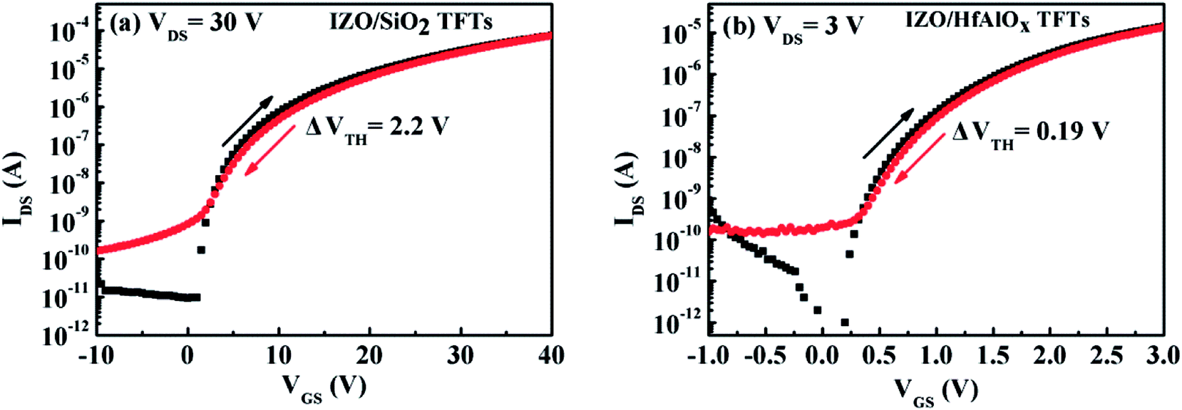 | ||
| Fig. 9 Transfer characteristics of (a) IZO/SiO2 TFTs and (b) IZO/HfAlOx TFTs. | ||
To achieve manufacturability of IZO-based TFT, it is crucial to solve the problems of the threshold-voltage (VTH) shift of the transistor with time under prolonged bias. Any shift in the threshold voltage of the driving transistor under gate and drain-bias stress conditions will cause a change in its output drain current, leading to circuit malfunction. Thus, device degradation due to bias-induced instability is a critical issue that must be solved. To investigate the bias stability of the IZO/HfAlOx TFTs, positive bias stress (PBS) tests were performed with the source and drain connected to the ground (VDS = 0 V). Fig. 10a shows the evolution of typical transfer characterization of the 450 °C-annealed IZO/HfAlOx TFTs subjected to a positive gate-bias voltage of 1 V for different stress time at room temperature (T = 25 °C). It can be observed that a parallel shift of the transfer curve toward the positive direction, and the evolution of the shift is from rapid to slow with stress time increasing, indicating there is no additional defect creation at the channel/dielectric interface during bias stressing.4 After the transistor has undergone the gate-bias stressing, the negligible change in the SS and carrier mobility suggests that the creation of extra electron trapping states at the semiconductor/dielectric interface is not significant. At the same time, higher operation stability with a small threshold voltage shift (ΔVTH) of 0.52 V up to 7200 s for 450 °C-annealed IZO/HfAlOx TFTs has been detected, revealing that there are a small number of defects at the IZO/HfAlOx interface, which is confirmed by previous Dit data. The VTH is presented as a function of stress time on a logarithmic scale in Fig. 10b. Based on Fig. 10b, it can be noted that VTH is shifted significantly at the beginning of the bias stressing, and as the stress continues, VTH approaches a saturation value. The shift of VTH is not accompanied by the SS degradation (Fig. 10a), which indicates that the ΔVTH in IZO is attributed to the trapping of electrons in the interface or bulk dielectric layers with negligible creation of additional interface traps.52
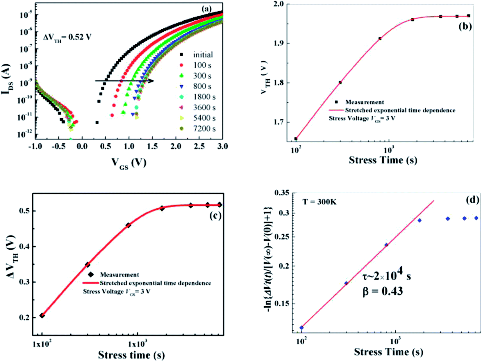 | ||
| Fig. 10 (a) Transfer curves of 450 °C annealed IZO/HfAlOx TFTs under PBS test. (b) The VTH as a function of stress time. (c) The time dependence of ΔVTH in the IZO/HfAlO TFTs under the bias stress of 3 V. (d) Threshold voltage shifts during bias stress at T = 300 K on a log10[−ln{ΔVt(t)/[V(∞) − V(0)] + 1}] vs. log10(t) plot. The data have been fitted to a stretched exponential {1 − exp[−(t/to)β], which reads a straight line in this format. | ||
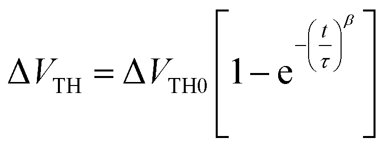
The investigation of the time dependence of ΔVTH can be used to confirm the dominant charge trapping mechanism causing the bias stress-induced ΔVTH in TFTs.53 To further investigate the bias stress-induced threshold voltage shift phenomenon in IZO/HfAlOx TFTs, the stress time dependences of ΔVTH under positive gate-bias voltage of 1 V at room temperature is examined and shown in Fig. 10c. The ΔVTH is defined as ΔVTH = VTH,t − VTH,i, where VTH,t is the VTH value at the measured time and VTH,i is the initial VTH. From Fig. 10c, it can be seen that the threshold voltage shifts rapidly and then is saturated quickly with the increase of stress time. Previous investigation on the bias stress-induced degradation of IGZO-based TFTs have indicated that the time dependence of ΔVTH under bias stresses in IGZO TFTs is followed by a logarithmic time-dependence model,53 but current work shows that the time dependence of ΔVTH can be fitted well with a stretched-exponential equation for all stress conditions, which has been developed to model the ΔVTH based on the charge trapping mechanism in α-Si TFT with high-k dielectric.52 The stretched exponential model of ΔVTH is defined as53
3.7 Resistor-loaded inverter
In spite of the improved electrical performance and traditional application in TFTs for solution-processed high-k gate dielectric films, the potential applications in more complex logic circuits were ignored. Encouraged by the excellent performance of 450 °C-derived IZO/HfAlOx TFTs, their applications in inverter were further explored to demonstrate the logic operations.53 A simple unipolar resistor-loaded inverter was fabricated by coupling the 450 °C-annealed IZO/HfAlOx TFTs with a 2.0 MΩ resistor. Fig. S6† shows the schematic diagrams and top views of the unipolar inverters, respectively. The Vin, Vout, and VDD represent input voltage, output voltage, and supplied voltage, respectively. Fig. 11a shows voltage transfer characteristic (VTC) of the inverters logic circuit with the VDD changing from 1 to 4.0 V. Distinct inverter characteristics are observed for the logic inverters at various VDD, in which the output voltage (Vout) is switched between VDD and 0 V when scanning input voltage (Vin) from 0 to 3 V. If the Vin is 0 V, the inverter operates in the off-stage, resulting in Vout close to VDD. If the Vin is 3.0 V, the inverter turns on, resulting in Vout close to the ground level. Thus, when the Vin operates with a low and logical 0 signal, the Vout responds a high and logical 1 signal. Likewise, when the Vin operates with a high and logical 1 signal, the Vout responds a low and logical 0 signal. These results indicate that our logic circuit demonstrates full swing characteristics. The voltage gain, defined as −∂Vout/∂Vin, is displayed in Fig. 11b as a function of VDD. A linear dependence between the voltage gain and VDD is observed. The maximum voltage gain of 4.46 has been obtained for VDD at 4.0 V, which is larger than that of previous reported oxide TFT circuits at the same supply voltage.55 It should be noted here that a voltage gain of 2.5 is sufficient to drive the next stage component in a logic circuit.55 The voltage swing, which is defined as [Vout,max − Vout,min]/VDD × 100%, increases slightly from 82% to 91% when increasing VDD from 1 to 4 V (Fig. 11c). The wider voltage swing of the inverter improves the noise margin characteristics, which makes the inverter run more reliably in the complex logic system. The improvement in voltage swing and gain with VDD can be attributed to a high capacitive efficiency.55 Another important parameter is the noise margin, which is usually used to evaluate the multistage circuit operation reliability. The noise margin calculation from VTC collected at VDD of 4 V is shown in the inset of Fig. 11c. The high (NMH) and low (NML) noise margins of the inverter are defined as NMH = VOH − VIH and NML = VIL − VOL,53 where VOH and VOL represent output high and low voltage; VIH and VOL represent input high and low voltage, respectively, while ∂Vout/∂Vin = −1. The NMH and NML of this inverter are calculated to be 2.48 V and 1.55 V at VDD of 4 V, revealing the potential application in multistage digital circuits.56 To investigate the alternative current (AC) characteristic of the inverter, the dynamic behavior at 1 Hz under AC square wave signal was measured, as shown in Fig. 11d. It can be noted that the as-constructed inverter exhibits good logic inversion action and responds well to the Vin square-wave signal, demonstrating its potential application in complex logic circuits, such as ring oscillators. | ||
| Fig. 11 (a) The VTCs and (b) signal gain of resistor-loaded inverter coupled with 450 °C-IZO/HfAlO TFTs. (c) The voltage gain and the voltage swing of the inverter at various VDD values. (d) Dynamic switching behavior of the inverter under square-waves at 1 Hz. The inset in (c) shows the noise margin calculation from VTC curve collected at 4 V VDD. | ||
4 Conclusions
In summary, fully solution-processed IZO TFTs based on HfAlOx dielectric have been fabricated successfully and annealing temperature dependent electrical properties of IZO/HfAlOx TFTs has been investigated systematically. Amorphous HfAlOx thin films annealed at 600 °C have shown a high transparency (>85%), low leakage current density (6.9 × 10⁻⁹ A cm−2 at 2 MV cm−1), and smooth surface. To verify the possible application of the HfAlOx thin films as dielectrics in low-temperature-processed CMOS logics, fully solution-derived IZO/HfAlOx TFTs have been successfully integrated to display a ultralow operating voltage of 3 V with optimized performance, including a high μsat of 5.17 cm2 V−1 S−1, an large Ion/Ioff of 7.5 × 10⁶, a small SS of 87 mV dec−1, an threshold voltage shift of 0.52 V under positive bias stress for 7200 s, respectively. To explore its potential application in complex logic circuits, a unipolar resistor-loaded inverter coupled with IZO/HfAlOx TFT has been built and excellent swing characteristic and well dynamic behavior have been obtained. Our strategy opens a simple and reliable path toward fabricating low-cost, low-power consumption, and large-area environmentally friendly oxide flexible electronics.Conflicts of interest
The authors declare no competing financial interest.Acknowledgements
The authors acknowledge the support from National Natural Science Foundation of China (11774001, 51572002), Open fund for Discipline Construction, Institute of Physical Science and Information Technology, Anhui University (S01003101), Technology Foundation for Selected Overseas Chinese Scholar, Ministry of Personnel of China (J05015131), Anhui Provincial Natural Science Foundation (1608085MA06).References
- J. F. Wager, Science, 2003, 300, 1245 CrossRef CAS PubMed.
- J. A. Rogers, Z. Bao, K. Baldwin, A. Dodabalapur, B. Crone, V. R. Raju, V. Kuck, H. Katz, K. Amundson, J. Ewing and P. Drzaic, Proc. Natl. Acad. Sci. U. S. A., 2001, 98, 4835 CrossRef CAS PubMed.
- K. Nomura, H. Ohta, A. Takagi, T. Kamiya, M. Hirano and H. Hosono, Nature, 2004, 432, 488 CrossRef CAS PubMed.
- G. X. Liu, A. Liu, F. K. Shan, Y. Meng, B. C. Shin, E. Fortunato and R. Martins, Appl. Phys. Lett., 2014, 105, 113509 CrossRef.
- E. Fortunato, P. Barquinha and R. Martins, Adv. Mater., 2012, 24, 2945 CrossRef CAS PubMed.
- R. Martins, P. Barquinha, A. Pimentel, L. Pereira and E. Fortunato, Phys. Status Solidi A, 2005, 202, R95 CrossRef CAS.
- P. Barquinha, A. Pimentel, A. Marques, L. Pereira, R. Martins and E. Fortunato, J. Non-Cryst. Solids, 2006, 352, 1749 CrossRef CAS.
- H. W. Park, K. Park, J. Y. Kwon, D. Choi and K. B. Chung, IEEE Trans. Electron Devices, 2017, 64, 159 CAS.
- C. G. Choi, S. Seo and B. Bae, Electrochem. Solid-State Lett., 2008, 11, H7 CrossRef CAS.
- B. Zhang, Y. Liu, S. Agarwal, M. Yeh and H. E. Katz, ACS Appl. Mater. Interfaces, 2011, 3, 4254 CrossRef CAS PubMed.
- K. H. Lee, M. S. Kang, S. Zhang, Y. Gu, T. P. Lodge and C. D. Frisbie, Adv. Mater., 2012, 24, 4457 CrossRef CAS PubMed.
- J. Kim, S. H. Lim and Y. S. Kim, J. Am. Chem. Soc., 2010, 132, 14721 CrossRef CAS PubMed.
- B. G. Son, S. Y. Je, H. J. Kim, C. K. Lee, A. Y. Hwang, J. Y. Won, J. H. Song, R. Choi and J. K. Jeong, Phys. Status Solidi RRL, 2013, 7, 485 CrossRef CAS.
- J. W. Zhang, G. He, L. Zhou, H. S. Chen, X. S. Chen, X. F. Chen, B. Deng, J. G. Lv and Z. Q. Sun, J. Alloys Compd., 2014, 611, 253 CrossRef CAS.
- C. Avis, Y. G. Kim and J. Jang, J. Mater. Chem., 2012, 22, 17415 RSC.
- A. Liu, Z. D. Guo, G. X. Liu, C. D. Zhu, H. H. Zhu, B. C. Shin, E. Fortunato, R. Martins and F. K. Shan, Adv. Electron. Mater., 2017, 3, 1600513 CrossRef.
- J. Ko, J. Kim, S. Y. Park, E. Lee, K. Kim, K. H. Lee and Y. S. Kim, J. Mater. Chem. C, 2014, 2, 1050 RSC.
- S. Park, B. L. Clak, D. A. Keszler, J. P. Bender, J. F. Wager, T. A. Reynolds and G. S. Herman, Science, 2002, 297, 65 CrossRef CAS PubMed.
- G. He, B. Deng, Z. Q. Sun, X. S. Chen, Y. M. Liu and L. D. Zhang, Crit. Rev. Solid State Mater. Sci., 2013, 38, 235 CrossRef CAS.
- G. He, Z. Q. Sun, G. Li and L. D. Zhang, Crit. Rev. Solid State Mater. Sci., 2012, 37, 131 CrossRef CAS.
- J. Gao, G. He, Z. Q. Sun, H. S. Chen, C. Y. Zheng, P. Jin, D. Q. Xiao and M. Liu, J. Alloys Compd., 2016, 667, 352 CrossRef CAS.
- Y. Yamamoto, K. Kita, K. Kyuno and A. Toriumi, Appl. Phys. Lett., 2006, 89, 032903 CrossRef.
- S. H. Bae, C. H. Lee, R. Clark and D. L. Kwong, IEEE Electron Device Lett., 2003, 24, 556 CAS.
- M. S. Joo, B. J. Cho, C. C. Yeo, S. S. Chan, S. J. Whoang, S. Mathew, L. K. Bera and D. L. Kwong, IEEE Trans. Electron Devices, 2003, 50, 2088 CrossRef CAS.
- J. Gao, G. He, M. Liu, J. G. Lv, Z. Q. Sun, C. Y. Zheng, P. Jin, D. Q. Xiao and X. S. Chen, J. Alloys Compd., 2017, 691, 504 CrossRef CAS.
- G. He, W. D. Li, H. H. Wei, S. S. Jiang, D. Q. Xiao, P. Jing and J. Gao, J. Alloys Compd., 2017, 695, 1591 CrossRef CAS.
- G. He and L. D. Zhang, J. Mater. Sci. Technol., 2007, 23, 433 CAS.
- A. Liu, Z. D. Guo, G. X. Liu, C. D. Zhu, H. H. Zhu, B. C. Shin, E. Fortunato, R. Martins and F. K. Shan, Adv. Electron. Mater., 2017, 3, 1600513 CrossRef.
- C. X. Fan, A. Liu, Y. Meng, Z. D. Guo, G. X. Liu and F. K. Shan, IEEE Trans. Electron Devices, 2017, 64, 4137 Search PubMed.
- J. M. Yu, G. X. Liu, A. Liu, Y. Meng, B. C. Shin, E. Fortunato and R. Martins, J. Mater. Chem. C, 2015, 3, 9509 RSC.
- Y. Meng, G. X. Liu, A. Liu, H. J. Sun, Y. Hou, B. Shin and F. K. Shan, RSC Adv., 2015, 5, 37807 RSC.
- K. Choi, M. Kim, S. Chang, T. Y. Oh, S. W. Jeong, H. J. Ha and B. K. Ju, Jpn. J. Appl. Phys., 2013, 52, 060204 CrossRef.
- J. H. Park, Y. B. Yoo, K. H. Lee, W. S. Jang, J. Y. Oh, S. S. Chae, H. W. Lee, S. W. Han and H. K. Baik, ACS Appl. Mater. Interfaces, 2013, 5, 8067 CrossRef CAS PubMed.
- G. He, L. D. Zhang, G. W. Meng, G. H. Li, Q. Fang and J. P. Zhang, J. Appl. Phys., 2007, 102, 094103 CrossRef.
- U. Myeonghun, H. I. Kwon, I. T. Cho, S. H. Jin and J. H. Lee, J. Korean Phys. Soc., 2014, 65, 286 CrossRef.
- W. Xu, H. Wang, F. Xie, J. Chen, H. Cao and J. B. Xu, ACS Appl. Mater. Interfaces, 2015, 7, 5803 CrossRef CAS PubMed.
- A. Liu, G. X. Liu, H. H. Zhu, F. Xu, E. Fortunato, R. Martins and F. K. Shan, ACS Appl. Mater. Interfaces, 2014, 6, 17364 CrossRef CAS PubMed.
- Y. J. Tak, S. J. Kim, S. Kwon, H. J. Kim, K. B. Chung and H. J. Kim, J. Mater. Chem. C, 2018, 6, 249 RSC.
- A. Liu, G. X. Liu, H. H. Zhu, B. C. Shin, E. Fortunato, R. Martins and F. K. Shan, RSC Adv., 2015, 5, 86606 RSC.
- K. Umeda, T. Miyasako, A. Sugiyama, A. Tanaka, M. Suzuki, E. Tokumitsu and T. Shimoda, J. Appl. Phys., 2013, 113, 184509 CrossRef.
- J. Y. Choi, S. S. Kim and S. Y. Lee, Appl. Phys. Lett., 2012, 100, 022109 CrossRef.
- Y. B. Yoo, J. H. Park, K. H. Lee, H. W. Lee, K. M. Song, S. J. Lee and H. K. Baik, J. Mater. Chem. C, 2013, 1, 1651 RSC.
- W. Xu, H. Wang, L. Ye and J. Xu, J. Mater. Chem. C, 2014, 2, 5389 RSC.
- B. N. Pal, B. M. Dhar, K. C. See and H. E. Katz, Nat. Mater., 2009, 8, 898 CrossRef CAS PubMed.
- J. S. Lee, Y. J. Kwack and W. S. Choi, ACS Appl. Mater. Interfaces, 2013, 5, 11578 CrossRef CAS PubMed.
- S. H. Jeong, Y. G. Ha, J. H. Moon, T. J. Marks and A. Facchetti, Adv. Mater., 2010, 22, 1346 CrossRef CAS PubMed.
- G. X. Jiang, A. Liu, G. X. Liu, C. D. Zhu, Y. Meng, B. Shin, E. Fortunato, R. Martins and F. K. Shan, Appl. Phys. Lett., 2016, 109, 183508 CrossRef.
- A. Liu, G. X. Liu, H. H. Zhu, H. J. Song, B. C. Shin, E. Fortunato, R. Martins and F. K. Shan, Adv. Funct. Mater., 2015, 25, 7180 CrossRef CAS.
- A. Javey, J. Guo, D. B. Farmer, Q. Wang, E. Yenilmez, R. G. Gordon, M. Lundstrom and H. J. Dai, Nano Lett., 2004, 4, 1319 CrossRef CAS.
- M. L. Geier, P. L. Prabhumirashi, J. J. McMorrow, W. Xu, J. W. Seo, K. Everaerts, T. J. Marks and M. C. Hersam, Nano Lett., 2013, 13, 4810 CrossRef CAS PubMed.
- J. H. Park, Y. B. Yoo, K. H. Lee, W. S. Jang, J. Y. Oh, S. S. Chae and H. K. Baik, ACS Appl. Mater. Interfaces, 2013, 5, 410 CrossRef CAS PubMed.
- I. T. Cho, J. M. Lee, J. H. Lee and H. I. Kwon, Semicond. Sci. Technol., 2009, 24, 015013 CrossRef.
- L. Zhu, G. He, W. D. Li, B. Yang, E. Fortunato and R. Martins, Adv. Electron. Mater., 2018, 4, 1800100 CrossRef.
- J. M. Lee, I. T. Cho, J. H. Lee and H. I. Kwon, Appl. Phys. Lett., 2008, 93, 093504 CrossRef.
- S. K. Lee, S. M. H. Kabir, B. K. Sharma, B. J. Kim, J. H. Cho and J. Ahn, Nanotechnology, 2014, 25, 014002 CrossRef PubMed.
- Y. Liu, X. Wan, L. Q. Zhu, Y. Shi and Q. Wan, IEEE Electron Device Lett., 2014, 35, 1257 CAS.
Footnote |
| † Electronic supplementary information (ESI) available. See DOI: 10.1039/c8ra07813k |
| This journal is © The Royal Society of Chemistry 2018 |