
 Open Access Article
 This Open Access Article is licensed under a Creative Commons Attribution-Non Commercial 3.0 Unported Licence
“Y”-shaped BP/PbS/PbSe nano-devices based on silicon carbide nanoribbons†
Lishu Zhang a,
Tao Lia,
Yangyan Jiang*a,
Hamidreza Arandiyan*b and
Hui Li*a
a,
Tao Lia,
Yangyan Jiang*a,
Hamidreza Arandiyan*b and
Hui Li*a
aKey Laboratory for Liquid-Solid Structural Evolution and Processing of Materials, Ministry of Education, Shandong University, Jinan 250061, People's Republic of China. E-mail: yanyan.jiang@sdu.edu.cn; lihuilmy@hotmail.com; Tel: +86-531-883-99579
bLaboratory of Advanced Catalysis for Sustainability, School of Chemistry, The University of Sydney, Sydney 2006, Australia. E-mail: hamid.arandiyan@sydney.edu.edu.au
First published on 12th October 2018
Abstract
Quantum mechanics-based simulations have been undertaken to support the development and application of multi-functional nano-devices constructed from zigzag silicon carbide nanoribbons (zSiCNRs), boron phosphide (BP), nanoribbons (zBPNRs), and Pb-chalcogenide (PbS, PbSe) nanoribbons. We explore the effect of gate voltage on the electronic performance of the devices. Symmetric I–V characteristics, spin polarization properties, NDR effects, and high rectification ratios are observed among these devices. The effects of the angle, length and width of the constructed nanoribbon are also studied. The results show that the width of the nanoribbons can have a substantial influence on their electronic performance. These results provide a crucial simulation input to help guide the design of multi-functional nano-devices built from hybrid SiC–BP/PbS/PbSe nanostructures, and this research is essential for better understanding of their electronic transport properties.
Introduction
Modern SiC technologies have led to a rapid improvement in the practical fabrication of SiC devices, such as photodiodes,1 high-temperature sensors,2 high-power devices,1,3,4 and microwave devices.5,6 This is derived from the fact that in carbon sp2 hybridization is more stable, while in silicon the preferable hybridization is sp3, hence, SiC has unique physical and electronic properties, and it is an ideal material for manufacturing electronic devices.7–9 2D materials have been attracting more and more attention in recent years. Graphene, particularly in the form of zigzag-edged nanoribbons (zGNRs), has been regarded as having promising potential for nano-devices. Similar to graphene,8,10 zigzag-edged SiC nanoribbons (zSiCNRs) are also found to have some unique and excellent properties, such as a honeycomb-like structure which is one-atom thick. In addition, zSiCNRs can exhibit magnetic characteristics with very small magnetic moments according to previous work.11,12 And zSiCNRs also present metallic or semiconducting phenomena, which depend on the width of the nanoribbon. All of the previous studies indicate that zSiCNRs are promising for both electronic and spintronic applications.7,11,122D materials have significant advantages in low-dimensional scientific research and nanoscale device application, which has aroused considerable interest in recent years. For example, Alejandro et al. predicted that boron phosphide (BP) nanosheets had intermediary electronic properties between those of graphene and BN systems.13 Although zigzag BP nanoribbons (zBPNRs) and zSiCNRs own the same crystal structure and similar lattice constant, their electronic properties are different because of the difference of C, Si, B, P electronic structures. Both theoretical and experimental works have indicated BP is a promising ideal candidate to adapt to electronic devices in future. For example, moderate band gap and high carrier mobility can coexist in h-BP.14,15 Encouragingly, BP film have been synthesized on aluminum nitride (0001)/sapphire substrate by chemical vapor deposition.16
Recently, other two-dimensional Pb-chalcogenide (PbS, PbSe) systems have been prepared by interfacial nanoscale assembly.17,18 which is a new potential photoelectric materials owning to the high symmetry of its rock-salt structure19 with a direct band gap of 0.41 eV,20 leading to the dependence of its optical behavior on temperature,21 efficient photon energy carrier multiplication22–24 and so on. Due to these characters, PbS-based nanomaterials possess wide applications in functional diodes,25,26 detectors,27 single electron devices,28 optical switches,29 optical amplification,30 telecommunication,31 biological imaging32 and nonlinear optics.33,34 As for the same family member, PbSe is also proved to be a good option for the next generation of electronic device since it possesses excellent electronic properties.35 In the last few years, many exciting contributions have emerged on nanoscale PbSe field. Fu et al. achieved the stability enhancement of PbSe colloidal QDs.36 And n- and p-channel thin film field-effect transistors made by PbSe were reported by Talapin,37 confirming the possibility of utilizing PbSe to fabricate the electronic device.
These four materials characteristics suggest that they have potential to play an important role in nano-devices in the future. We wonder whether we can integrate their excellence together to construct a novel “Y”-shaped hybrid structure as a multi-functional nano-device.38 Here, we propose a “Y”-shaped nanostructures consisting of zSiCNRs, zBPNRs, zPbSNRs and zPbSeNRs to construct nano-devices for potential applications.
Results and discussion
Fig. 1 shows the schematic of the computational model which illustrates four types of “Y”-shaped tri-wing hybrid structures composed of (a) zSiCNRs, (b) zBPNRs, (c) zPbSeNRs and (d) zPbSNRs, denoted tri-SiC, tri-SiC–BP, tri-SiC–PbSe and tri-SiC–PbS respectively. All the structures are passivated with hydrogen. The three legs lie in the xy plane, and z is the transport direction of 1D structures. SiCNRs, BPNRs, PbSeNRs and PbSNRs are classified by the number of zigzag SiC, BP, PbSe or PbS chains (N) along the y-axis and are denoted as NzSiCNR, NzBPNR, NzPbSeNR and NzPbSNR, respectively. The tri-SiC includes three 4zSiCNRs with two Si edges and one C edges connected by sp3 hybridization, whereas two 4zSiCNRs and one 4zPbSNR (4zBPNR) with one Si edge connected to one S(P) edge make up the tri-SiC–PbS (tri-SiC–BP). And the tri-SiC–PbSe has the similar structure to tri-SiC–PbS. We repeat configuration three times along the z-axis. The angle value between two up legs in the Y-shaped structure is 120° in xy plane. Based on previous studies of three-wing GNR, these hybrid structures should be fairly stable to resist external interference.39,40 In addition, these “Y”-shaped tri-wing hybrids may show interesting electronic characteristics due to hybridization between the three wings. As shown in Fig. 2, the “Y”-shaped tri-wing hybrid structure is sandwiched between two graphene electrodes in a field effect transistor (FET) configuration where the transverse gate voltage (Vg) is only applied on the “Y”-shaped tri-wing hybrid structure.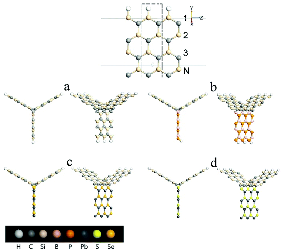 | ||
| Fig. 1 Schematic of the computational model and structures of (a) tri-SiC, (b) tri-SiC–BP, (c) tri-SiC–PbSe, and (d) tri-SiC–PbS. SiCNRs, BPNRs, PbSeNRs and PbSNRs are classified by the number of zigzag SiC, BP, PbSe or PbS chains (N) along the y-axis and are denoted as NzSiCNR, NzBPNR, NzPbSeNR and NzPbSNR, respectively. The dashed box denotes the unit cell. | ||
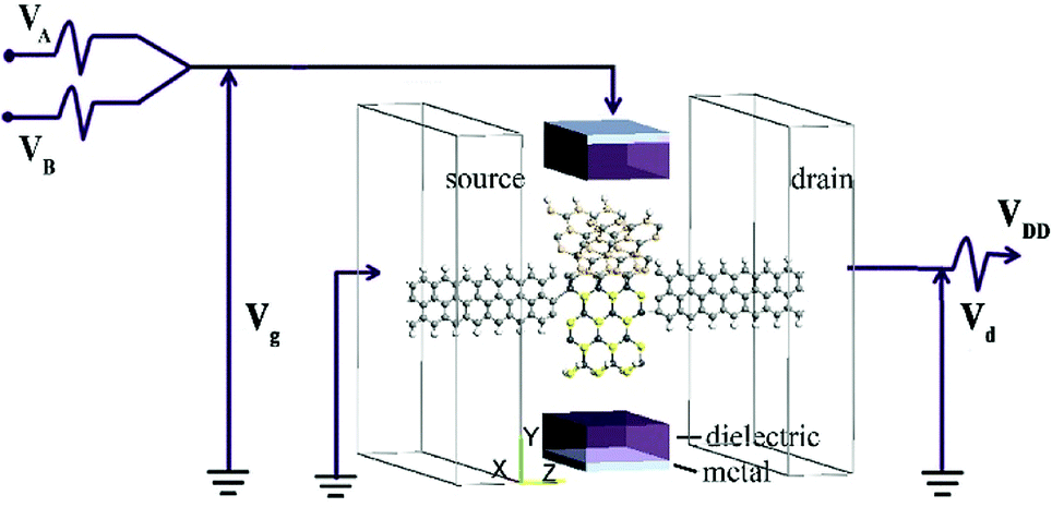 | ||
| Fig. 2 Electrical circuit diagram of a dual input (A and B) logic gate. Between the four electrodes is the electronic device composed of two contacts (source and drain), a nano-device and gate electrodes. The dielectric constant and the thickness of dielectric layers are 3.9ε0 and 4.0 Å. | ||
First of all, the current–voltage characteristics of the tri-SiC, tri-SiC–BP, tri-SiC–PbS and tri-SiC–PbSe at various gate voltage are shown in Fig. 3. The results show that the effect of gate electrodes on current is different among the four models.
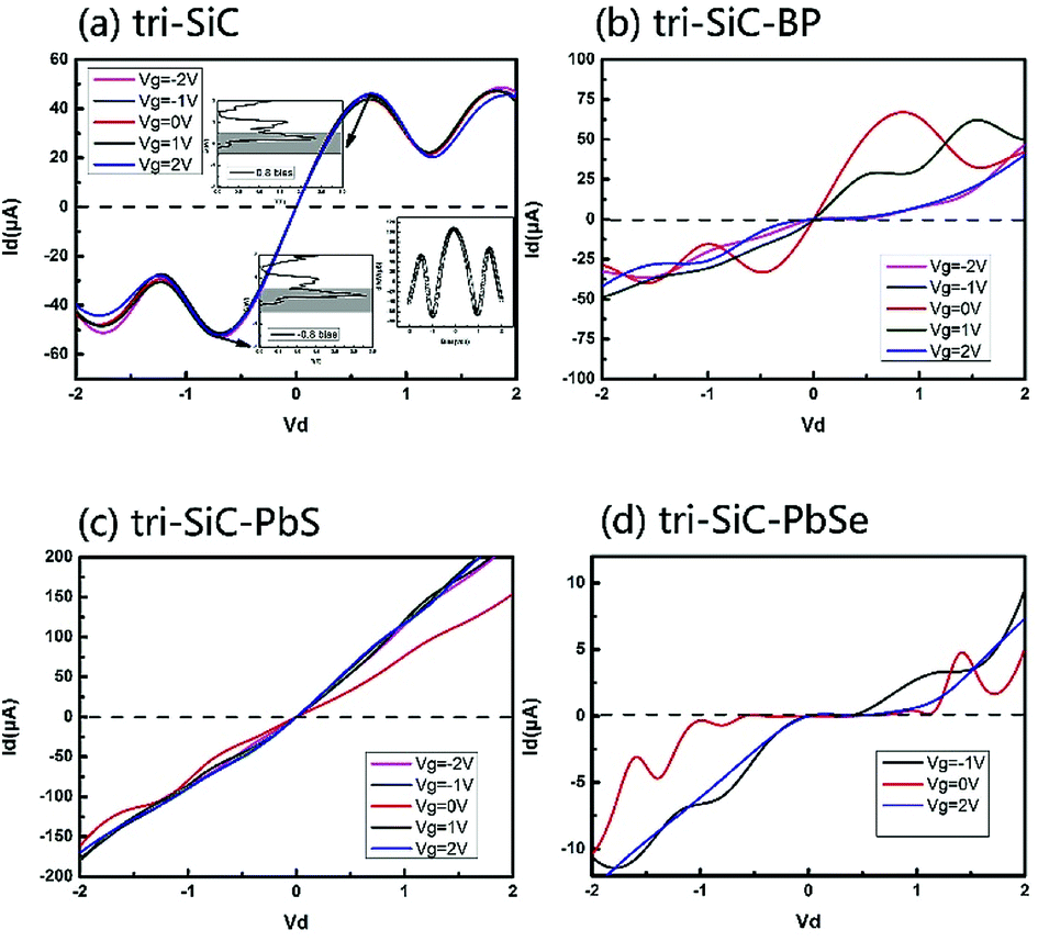 | ||
| Fig. 3 (a) Current–voltage characteristics of the tri-SiC device at different gate voltage. The insets show transmission spectra at two individual voltage points and the corresponding conductance curve of the tri-SiC at equilibrium state. The grey area represents the bias window. (b) Current–voltage characteristics of the tri-SiC–BP device at different gate voltage. (c) Current–voltage characteristics of the tri-SiC–PbS device at different gate voltage. (d) Current–voltage characteristics of the tri-SiC–PbSe device at different gate voltage. | ||
For the device tri-SiC, the I–V curves are symmetrical at the zero point, the current is not sensitive to the change of the gate voltage. For tri-SiC–BP, however, the I–V curves of the tri-SiC–BP do not follow the Ohm's law. For example, when Vg = 0 and Vg = 1 V, both two curves offer upgrade firstly then descending latter tendency at positive bias. This phenomenon of upward and downward movement is what we called the negative differential resistance (NDR) effect. This NDR effect due to the quantum effect.41,42 While for tri-SiC–PbS, it follows Ohm's law that I–V curve almost exhibits linear relation. The slope of the I–V curve is markedly elevated when the gate voltage is applied, and the slope would not change any matter how much gate voltage applied. Specifically, as for the tri-SiC–PbSe, it is clear that the current is affected strongly by the different gate potential. A large zero-current Coulomb gap and current plateau are presented, possessing the characteristic of Coulomb blockade and Coulomb staircase. The tri-SiC–PbSe has obvious on- off state and the current is cut off around [−0.5, 1.0] region at Vg = 0 V, thus, being as “on” and “off” states of the switch. Interestingly, the on–off states region can be regulated by the gate voltage. As can be seen that when applied the gate voltage (positive or negative gate bias), the off region reduces and the operate region expands.
Now, we probe into the origin of the symmetrical I–V feature of the tri-SiC. Its current–voltage characteristics at equilibrium state are illustrated in Fig. 3(a). As the integral area of the transmission curve within the bias window determines the current, we draw the transmission spectra at two inflection points on the I–V curve in insets of Fig. 3(a). It is found that the inflection point at 0.6 V corresponds well to another inflection point located at −0.6 V. And the case at bias 0.6 and 1.2 is also the same, showing typical marvelous symmetry. As depicted in the inset of Fig. 3(a), the conductance curve of the tri-SiC device exhibits “W”-shaped-characteristics which shows completely vertical symmetry at zero point, corresponding well to the symmetry of I–V curves.
In order to explore the spin characteristics of the tri-SiC, the electronic structures and the density of states (DOS) at Vg = 0 V and Vg = 2 V are shown in Fig. 4. We select two bands above and below the Fermi energy level closely which locate at Γ point for both up-spin and down-spin species. The corresponding Bloch states at the Γ point indicate that only the valence band results from the coupling of the three SiC wings. But the presence of conductance band is due to the p states of the Si atoms at the Si edge of the three SiC nanoribbons. From Fig. 4(h), it can be seen that the main peak of the down-spin DOS around Fermi level shifts to the right more easily compared to that of up-spin, which corresponds well to their band structures. We can see that p orbit mainly contributes to DOS and the down-spin is stronger than the up-spin. And the down-spin state when the applied gate voltage Vg is 2 V has more distinct contribution to DOS than that when Vg is 0 V. To reveal the relationship between the contact of two types of atoms and the high electron performance of the tri-SiC device, we further calculated the EDD (electron differential density), as shown in Fig. 4(f and g). An interaction between the C and Si atomic surfaces shows that the change in electron density is non-negligible after self-consistent simulation at its boundary. The blue color in the EDD map means very small value of EDD, indicating high interactions produce enough electron density, but pink color means big value of EDD. We can know that the center connection is stronger than the three wings, and the difference between self-consistent charge density and atomic charge density of Si atom is greater than that of C atom.
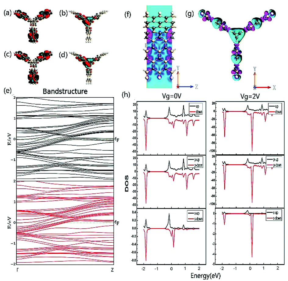 | ||
| Fig. 4 The structures and transport properties of tri-SiC device. (a and b) The Bloch states of up-spin at the Γ point, respectively. (c and d) The Bloch states of down-spin at the Γ point, respectively. (e) The band structures of up-spin (black line) and down-spin (red line), respectively. (f and g) Electron difference density of tri-SiC device in different perspective. (h) Density of states of up-spin electrons (black line) and down-spin electrons (red line) for the device tri-SiC at Vg = 0 V and Vg = 2 V, respectively. The Fermi level is set at zero in the energy scale. | ||
Fig. 5(a–c) shows the transmission spectra and DOS of the tri-SiC–BP at zero bias when Vg = 0 V, −2 V and 1 V, respectively. From the figure we find peaks at the DOS in the vicinity of the Fermi level correspond partially to that at transmission spectra, and the gate voltage has distinct influence on the electron state around Fermi level. In order to make it clear, we further calculate LDOS at EF = 1.1 eV, −0.5 eV and −1.5 eV when Vg = 0, −2 and 1 V respectively, since these three typical energy values accord well with the DOS and transmission spectra. We can see from Fig. 5(d) that the LDOS of electrons in device tri-SiC–BP without gate voltage delocalizes at the SiC region, demonstrating that the BP nanoribbons have hardly any contribution to the DOS in this condition. However, when the applied gate voltage Vg = −2 V or Vg = 1 V, the biggest LDOS moves to the BP nanoribbons bottom as shown in Fig. 4(e and f), showing that the main electrons transport pathway transfers from the SiC to BP nanoribbons which might lead to a big current change.
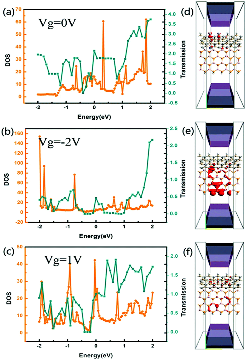 | ||
| Fig. 5 (a–c) Density of states and transmission spectra for the device tri-SiC–BP at different bias of Vg = 0 V, Vg = −2 V and Vg = 1 V, respectively. The Fermi level is set at zero in the energy scale. (d–f) LDOS for the device tri-SiC–BP at EF = 1.1 eV, −0.5 eV and −1.5 eV when Vg = 0, −2 and 1 V, respectively. The energy origin is set to be the average Fermi level EF and isosurface showing the LDOS of the corresponding junctions at 0.1 eV. The isosurface shown corresponds to 0.0005 states per Å3 per eV. | ||
Fig. 6 illustrates the LDOS of the device tri-SiC–PbS without gate electrode applied and with different gate voltage applied with type of n and p. It is obviously seen from Fig. 6(a) that the LDOS of electrons mainly delocalizes on the PbS nanoribbons, especially on their bottom Pb and S atoms. After applied gate electrodes, the LDOS of electrons in PbS nanoribbon almost disappears except a few atoms having less contribution to the DOS and most of them transfer to SiC as shown in Fig. 6(b). This illustrates the gate voltage can block the electrons transport through the PbS nanoribbon in device tri-SiC–PbS significantly. So, the conductance of tri-SiC–PbS can be tuned by an applied voltage, suggesting this could be used as a gate-electrode to control the current switching. Compared to Fig. 6(b), the distribution of LDOS is nearly not changing when applied a reverse gate voltage, depicted in Fig. 6(c), interpreting why I–V curves almost unchanged when the gate voltage changes. Based on this kind of gate voltage insensitive property, when we use this device as a current switching, we can tune it regardless of the value and direction of the gate voltage.
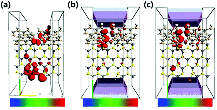 | ||
| Fig. 6 LDOS of the tri-SiC–PbS at (a) Vg = 0 V, (b) Vg = 2 V and (c) Vg = −2 V with an isovalue of 0.04. The energy origin is set to be the average Fermi level EF and isosurface showing the LDOS of the corresponding junctions at 0.1 eV. The isosurface shown corresponds to 0.0005 states per Å3 per eV. | ||
Fig. 7 shows the rectification ratio and the transmission spectra of the device tri-SiC–PbSe. It can be seen that its I–V curves show distinct asymmetric characteristics which can be explained by the rectification ratio. Rectification ratio is the ratio of current to positive voltage and negative voltage when the absolute value of the voltage is the same, that is, RR(V) = |I(V)/I(−V)|, as shown in Fig. 7(a). We define the rectification ratio RR(V) > 1 is the forward rectifying behavior and RR(V) < 1 is the reverse rectifying behavior. It can be seen from Fig. 7(a) that the tri-SiC–PbSe appears strong forward rectifying behavior when Vg = 0 V, which gains the maximum rectification ratio of 4.43. However, it appears weak reverse is rectifying behavior after applied gate voltage. To understand the underlying physics behind the rectifying effect, its transmission spectra are calculated. As depicted in Fig. 7(b), the transmission curve within the bias window has a larger integrating area at a positive bias of 1.0 V than that at a negative bias of −1.0 V, resulting in the maximum forward rectification ratio when no gate voltage applied (Vg = 0 V). When negative bias Vg = −1 or positive bias Vg = 2 V, more than one transmission peaks move into the bias window and increase significantly. However, the peaks at the negative bias window play an important role, and the magnitude is larger than that at the positive window, resulting in a change in the rectification ratio, as illustrated in Fig. 7(c and d).
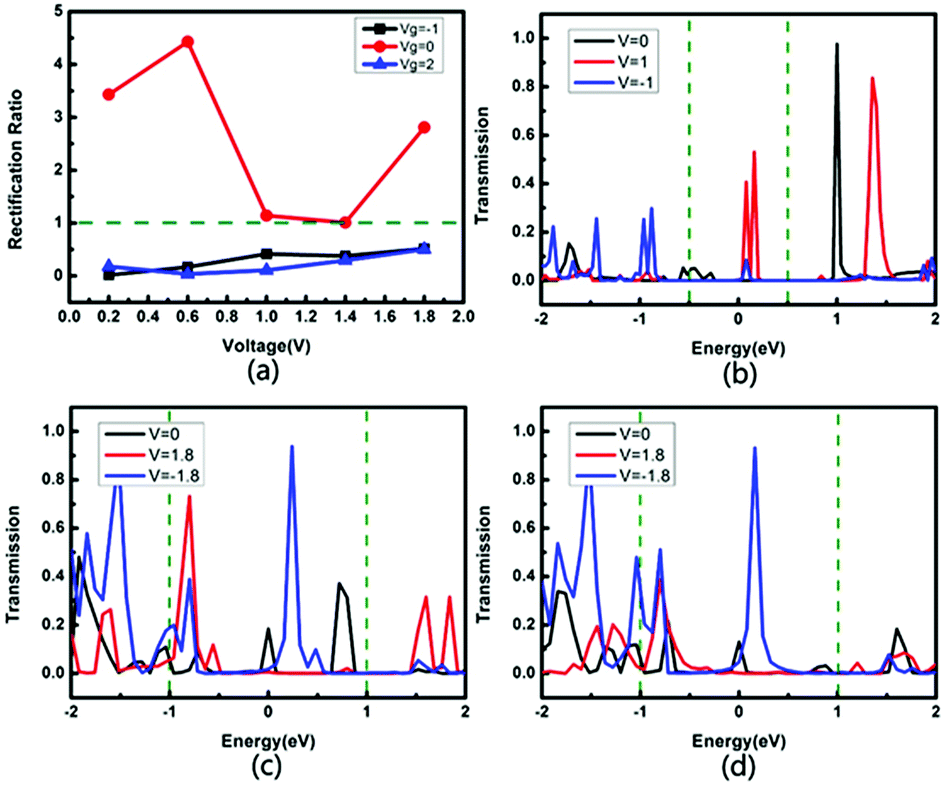 | ||
| Fig. 7 (a) Rectification ratio for the device tri-SiC–PbSe. Transmission spectra for the device tri-SiC–PbSe at (b) Vg = 0 V, (c) Vg = −1 V and (d) Vg = 2 V. | ||
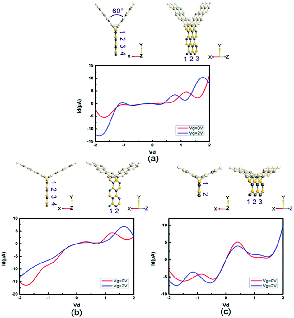
Moreover, we study the effects of the angle, width and length on the electronic performance of the devices. Since I–V curves are one of the most intuitive manners of electronic performance, we calculate the I–V characteristics of PbS-based and PbSe-based devices, as shown in Fig. 8 and 9, respectively. First, we change the angle between the two SiC wings from 120° to 60°, as displayed in Fig. 8(a) and 9(a). It can be seen that the change of angle does not have significant influence on their behaviors. It is roughly similar to I–V curves of the prototypes, especially for the angle-changed tri-SiC–PbSe. And gate voltage still does not affect the angle-changed tri-SiC–PbS but has distinctive effect on the angle-changed tri-SiC–PbSe. Furthermore, we change the length of PbS and PbSe nanoribbons from three units to two units, as shown in Fig. 8(b) and 9(b). It can be seen that small changes are observed, but still can be ignored. I–V characteristics of the changed structures still follow the features of prototypes. We also change the number of zigzag PbS or PbSe chains (N) from four to two in order to improve the width of nanoribbons, as illustrated in Fig. 8(c) and 9(c). Strong changes of electronic performance emerge. Distinctive NDR effect appears when changed the length of PbS nanoribbon in tri-SiC–PbS, which shows linear relation. In a word, angle and length of nanoribbon have seldom influence on electronic performance, but width can have strong effect.
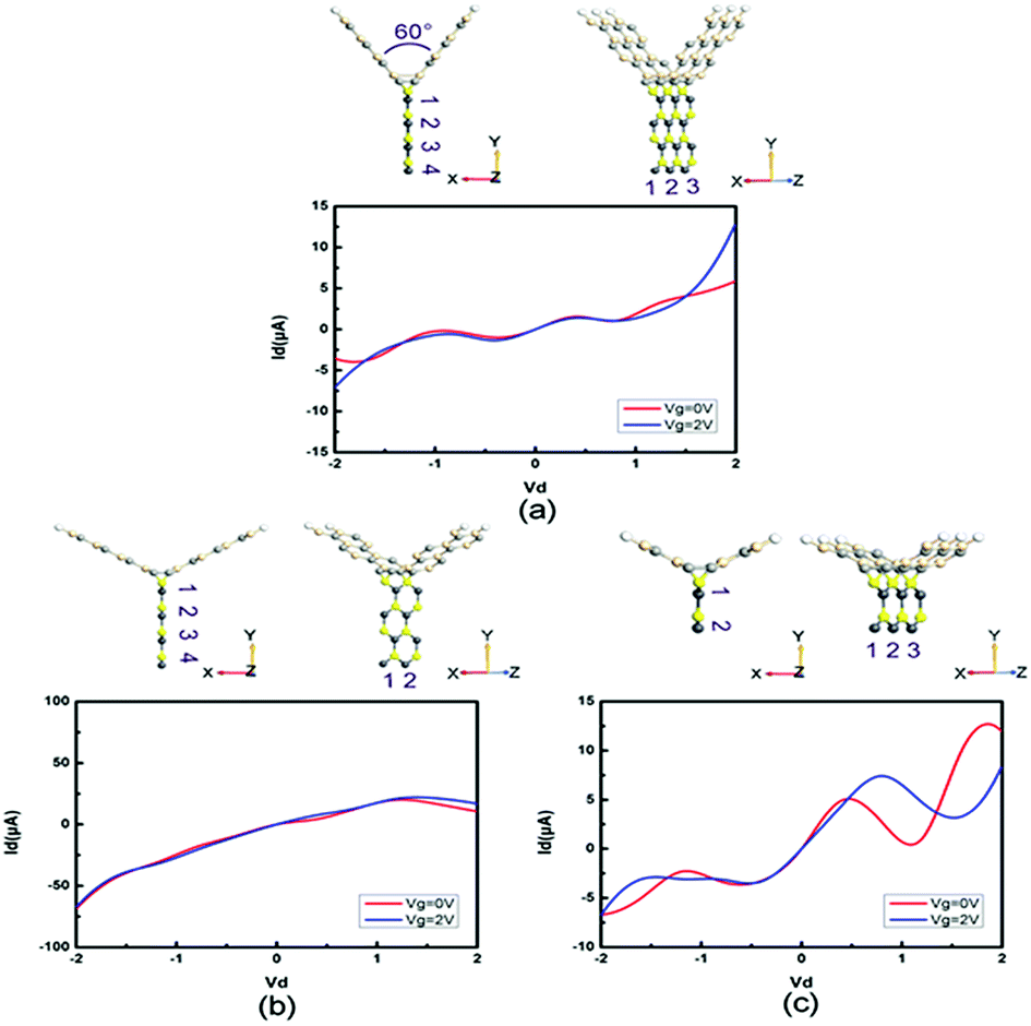 | ||
| Fig. 8 (a) The structures and I–V characteristics of tri-SiC–PbS when changing the angle between two SiC nanoribbons from 120° to 60°. The angle after change is labeled in the figure. (b) The structures and I–V characteristics of tri-SiC–PbSe when changing the length of the PbS nanoribbon from three to two. (c) The structures and I–V characteristics of tri-SiC–PbSe when changing the width of the PbS nanoribbon from four to two. The numbers represent the number of zigzag chains in each branch wing after change. | ||
 | ||
| Fig. 9 (a) The structures and I–V characteristics of tri-SiC–PbSe when changing the angle between two SiC nanoribbons from 120° to 60°. The angle after change is labeled in the figure. (b) The structures and I–V characteristics of tri-SiC–PbSe when changing the length of the PbSe nanoribbon from three to two. (c) The structures and I–V characteristics of tri-SiC–PbSe when changing the width of the PbSe nanoribbon from four to two. The numbers represent the number of zigzag chains in each branch wing after change. | ||
Methods
In this work, we adopt density functional theory (DFT) method and non-equilibrium Green's function (NEGF) formalism as implemented in Atomistix ToolKit (ATK) software package.43 The mesh k points are set as 1 × 1 × 50.38 The mesh cutoff is 75 Ha. The electron temperature is set to 300 K. In order to avoid the interaction between periodic images, all structures are modeled in a supercell with vacuum layers of at least 15 Å between neighboring cells. The exchange-correlation potential is described by the Perdew–Burke–Ernzerhof parameterization of the generalized gradient approximation (GGA–PBE) or spin-dependent generalized gradient approximation (SGGA–PBE). Local atomic numerical orbits with double-zeta single polarized basis and norm-conserving pseudopotentials are used. The simulated system can be divided into three parts: one is central scattering region, others are semi-infinite right and left electrodes. We also add gate electrodes with dielectric layers which are an oxide. Before calculations of electronic transport properties, the geometry of model is first optimized until all residual forces on each atom are smaller than 0.05 eV Å−1. More detail can refer to ESI.†Conclusions
The electronic properties of “Y”-shaped BP/PbS/PbSe nanodevices based on silicon carbide nanoribbons were revealed using quantum mechanics-based simulations. For the device tri-SiC, the current is not sensitive to the change of the gate voltage. All the I–V curves under different gate voltage are symmetrical at the zero point and “W”-shaped conductance characteristics are found. In addition, significant spin polarization characteristics were observed, making it potential building block for spintronics. As for the device tri-SiC–BP, strong NDR effect appears because of the change of the transport pathway under the gate bias, which might be utilized in the frequency multipliers and oscillators. And device tri-SiC–PbS could be used as a current switching not controlled by gate voltage. While the device tri-SiC–PbSe shows obvious on and off states which could be used as switching and the rectifying circuits. The effects of the angle, length and width of the constructed nanoribbons are also studied. The results show that angle and length of nanoribbon have seldom influence on electronic performance, but width can have substantial effect. This study may provide theoretical guidance for the exploration of multi-functional nano-devices in a new way.Conflicts of interest
There are no conflicts to declare.Acknowledgements
The authors would like to acknowledge the support from the National Natural Science Foundation of China (Grant No. 51671114) and the Fundamental Research Funds of Shandong University (Grant No. 2018CJ047). This work is also supported by the Special Funding in the Project of the Taishan Scholar Construction Engineering and Qilu Young Scholar Program of Shandong University.Notes and references
- S. Castelletto, B. C. Johnson, N. Stavrias, T. Umeda, A. Gali and T. Ohshima, Nat. Mater., 2014, 13, 151 CrossRef CAS PubMed.
- K. V. Emtsev, A. Bostwick, K. Horn, J. Jobst, G. L. Kellogg, L. Ley, J. L. Mcchesney, T. Ohta, S. A. Reshanov and J. Röhrl, Nat. Mater., 2008, 8, 203 CrossRef PubMed.
- C. E. Weitzel, J. W. Palmour, C. H. Carter and K. Moore, IEEE Trans. Electron Devices, 1996, 43, 1732–1741 CrossRef CAS.
- J. P. Alper, M. S. Kim, M. Vincent, B. Hsia, V. Radmilovic, C. Carraro and R. Maboudian, J. Power Sources, 2013, 230, 298–302 CrossRef CAS.
- Z. C. Feng, A. J. Mascarenhas, W. J. Choyke and J. A. Powell, J. Appl. Phys., 1988, 64, 3176–3186 CrossRef CAS.
- W. F. Koehl, B. B. Buckley, F. J. Heremans, G. Calusine and D. D. Awschalom, Nature, 2011, 479, 84–87 CrossRef CAS PubMed.
- J. M. Zhang, F. L. Zheng, Y. Zhang and V. Ji, J. Mater. Sci., 2010, 45, 3259–3265 CrossRef CAS.
- Y. Ding and Y. Wang, Appl. Phys. Lett., 2012, 101, 109 Search PubMed.
- J. M. Morbec and G. Rahman, Phys. Rev. B: Condens. Matter Mater. Phys., 2013, 87, 115428 CrossRef.
- X. Zheng, X. Chen, L. Zhang, L. Xiao, S. Jia, Z. Zeng and H. Guo, 2D Mater., 2017, 4, 025013 CrossRef.
- L. Ping and Y. L. Jin, J. Phys. Chem. C, 2009, 113, 12637–12640 CrossRef.
- L. Sun, Y. Li, Z. Li, Q. Li, Z. Zhou, Z. Chen, J. Yang and J. G. Hou, J. Chem. Phys., 2008, 129, 11754 Search PubMed.
- A. López-Castillo, Int. J. Quantum Chem., 2012, 112, 3152–3157 CrossRef.
- H. L. Zhuang and R. G. Hennig, Appl. Phys. Lett., 2012, 101, 666 Search PubMed.
- D. Çakir, D. Kecik, H. Sahin, E. Durgun and F. M. Peeters, Phys. Chem. Chem. Phys., 2015, 17, 13013–13020 RSC.
- B. Padavala, C. D. Frye, X. Wang, Z. Ding, R. Chen, M. Dudley, B. Raghothamachar, P. Lu, B. N. Flanders and J. H. Edgar, Cryst. Growth Des., 2016, 16, 981 CrossRef CAS.
- W. H. Evers, B. Goris, S. Bals, M. Casavola, G. J. De, R. R. Van, M. Dijkstra and D. Vanmaekelbergh, Nano Lett., 2013, 13, 2317 CrossRef CAS PubMed.
- M. P. Boneschanscher, W. H. Evers, J. J. Geuchies, T. Altantzis, B. Goris, F. T. Rabouw, S. A. van Rossum, V. D. Z. Hs, L. D. Siebbeles and T. G. Van, Science, 2014, 344, 1377 CrossRef CAS PubMed.
- D. Zherebetskyy, M. Scheele, Y. Zhang, N. Bronstein, C. Thompson, D. Britt, M. Salmeron, P. Alivisatos and L. W. Wang, Science, 2014, 344, 1380 CrossRef CAS PubMed.
- S. K. Yadav and P. Jeevanandam, Opt. Mater., 2015, 46, 209–215 CrossRef CAS.
- H. Zhao, H. Liang, F. Vidal, F. Rosei, A. Vomiero and D. Ma, J. Phys. Chem. C, 2014, 118, 20585–20593 CrossRef CAS.
- M. Aerts, T. Bielewicz, C. Klinke, F. C. Grozema, A. J. Houtepen, J. M. Schins and L. D. A. Siebbeles, Nat. Commun., 2014, 5, 3789 CrossRef PubMed.
- W. W. Scanlon, J. Phys. Chem. Solids, 1959, 8, 423–428 CrossRef CAS.
- S. J. Oh, N. E. Berry, J. H. Choi, E. A. Gaulding, H. Lin, T. Paik, B. T. Diroll, S. Muramoto, C. B. Murray and C. R. Kagan, Nano Lett., 2014, 14, 1559 CrossRef CAS PubMed.
- B. N. Pal, I. Robel, A. Mohite, R. Laocharoensuk, D. J. Werder and V. I. Klimov, Adv. Funct. Mater., 2012, 22, 1741–1748 CrossRef CAS.
- I. Schnitzer, A. Katzir, U. Schiessl, W. J. Riedel and M. Tacke, J. Appl. Phys., 1989, 66, 5667–5670 CrossRef CAS.
- R. Saran, M. N. Nordin and R. J. Curry, Adv. Funct. Mater., 2013, 23, 4149–4155 CrossRef CAS.
- P. Jiang, Z. Liu, Y. Wang and S. Cai, Mol. Cryst. Liq. Cryst. Sci. Technol., Sect. A, 1999, 337, 317–320 CrossRef CAS.
- C. Liu, Y. K. Kwon and J. Heo, Appl. Phys. Lett., 2009, 94, 441 CrossRef.
- E. H. Sargent, Adv. Mater., 2005, 17, 515–522 CrossRef CAS.
- F. W. Wise, Acc. Chem. Res., 2000, 33, 773–780 CrossRef CAS PubMed.
- Y. Nakane, Y. Tsukasaki, T. Sakata, H. Yasuda and T. Jin, Chem. Commun., 2013, 49, 7584–7586 RSC.
- M. S. Neo, N. Venkatram, G. S. Li, W. S. Chin and J. Wei, J. Phys. Chem. C, 2009, 113, 19055 CrossRef CAS.
- J. H. Warner, N. Heckenberg and H. Rubinsztein-Dunlop, Mater. Lett., 2006, 60, 3332–3334 CrossRef CAS.
- R. D. Schaller and V. I. Klimov, Phys. Rev. Lett., 2004, 92, 186601 CrossRef CAS PubMed.
- C. Fu, H. Wang, T. Song, L. Zhang, W. Li, B. He, M. Sulaman, S. Yang and B. Zou, Nanotechnology, 2016, 27, 065201 CrossRef PubMed.
- D. V. Talapin and C. B. Murray, Science, 2005, 310, 86 CrossRef CAS PubMed.
- J. Dong, H. Li and L. Li, NPG Asia Mater., 2013, 5, e56 CrossRef CAS.
- L. Zhu, J. Wang, T. Zhang, L. Ma, C. W. Lim, F. Ding and X. C. Zeng, Nano Lett., 2010, 10, 494 CrossRef CAS PubMed.
- L. Ma, H. Hu, L. Zhu and J. Wang, J. Phys. Chem. C, 2011, 115, 6195–6199 CrossRef CAS.
- L. Zhang, Y. Li, T. Li and H. Li, RSC Adv., 2018, 8, 1519–1527 RSC.
- L. Zhang, X. Dai, Y. Zhou, Z. Zhao, L. Yin and H. Li, Comput. Mater. Sci., 2017, 136, 198–206 CrossRef CAS.
- X. F. Yang, W. Q. Zhou, X. K. Hong, Y. S. Liu, X. F. Wang and J. F. Feng, J. Chem. Phys., 2015, 142, 323 Search PubMed.
Footnote |
| † Electronic supplementary information (ESI) available. See DOI: 10.1039/c8ra07372d |
| This journal is © The Royal Society of Chemistry 2018 |