
 Open Access Article
 This Open Access Article is licensed under a Creative Commons Attribution-Non Commercial 3.0 Unported Licence
Low temperature-processed ZnO thin films for p–n junction-based visible-blind ultraviolet photodetectors
Hanna B.ab,
Surendran K. P. ac and
Narayanan Unni K. N.*ab
ac and
Narayanan Unni K. N.*ab
aAcademy of Scientific and Innovative Research (AcSIR), CSIR-NIIST Campus, Thiruvananthapuram 695019, India. E-mail: unni@niist.res.in
bPhotosciences and Photonics Section, Chemical Sciences and Technology Division, CSIR-National Institute for Interdisciplinary Science and Technology, Thiruvananthapuram-695019, Kerala, India
cFunctional Materials Section, Materials Science and Technology Division, CSIR-National Institute for Interdisciplinary Science and Technology, Thiruvananthapuram-695019, Kerala, India
First published on 6th November 2018
Abstract
Ultraviolet (UV) photodetectors have drawn extensive attention due to their numerous applications in both civilian and military areas including flame detection, UV sterilization, aerospace UV monitoring, missile early warning, and ultraviolet imaging. Zinc oxide (ZnO)-based UV detectors exhibit remarkable performance; however, many of them are not visible-blind, and the fabrication techniques involve a high-temperature annealing step. Here, we fabricated a p–n junction photodiode based on annealing-free ZnO thin films prepared from ZnO nanoparticles and N,N′-di(1-naphthyl)-N,N′-diphenyl-(1,1′-biphenyl)-4,4′-diamine (NPB). NPB was chosen due to its transparent nature in the visible region and high hole mobility. The ZnO nanoparticles and thin films were characterized by UV-visible absorption spectroscopy, atomic force microscopy (AFM), scanning electron microscopy (SEM), dynamic light scattering (DLS) particle size analysis, Fourier-transform infrared (FTIR) spectroscopy, photoluminescence spectroscopy, XRD and profilometry. The device exhibited responsivity of 0.037 A/W and an external quantum efficiency (EQE) of 12.86% at 5 V bias under 360 nm illumination. In addition, with no biasing, the device exhibited an on–off ratio of more than 103 and a linear dynamic range (LDR) of 63 dB. A high built-in potential at the ZnO/NPB interface could be the reason for this performance at zero bias. The rise and fall times were 156 ms and 319 ms, respectively. The results suggest that a visible-blind UV photodetector with acceptable performance can be fabricated using annealing-free ZnO films, which may lead to the realization of flexible detectors due to the low-temperature processes involved.
Introduction
Ultraviolet (UV) detectors have great importance for the survival and development of humankind since excessive exposure to UV radiation causes skin cancer, damage to the immune system and acceleration of the aging process. UV photodetectors are optoelectronic devices that find a wide range of applications in different areas such as radiation detection, UV imaging, pollution monitoring, and space communications.1 Silicon and photomultiplier tube (PMT)-based UV photodetectors have received greater attention due to their high sensitivity, high signal-to-noise ratio and high responsivity. However, PMTs need high operating voltages and an ultra-high vacuum environment, and silicon photodetectors require filters to stop higher wavelength radiation during their operation.2 To circumvent these limitations, UV photodetectors are presently fabricated based on wide bandgap semiconductors such as ZnO,3–6 GaN,7 TiO2,8 diamond,9 and SiC.10 Among them, ZnO is the most suitable material for the fabrication of UV photodetectors due to its attractive properties such as high radiation tolerance, high break down voltage, low toxicity, high transparency, low cost, high electron mobility, large exciton binding energy (60 meV), high refractive index and versatile synthetic methods.11 These synthetic methods include molecular beam epitaxy (MBE), pulsed laser deposition (PLD), sputtering, chemical vapor deposition (CVD), and solution processing. Compared to all other techniques, solution processing is a simple and low-cost technique to produce high-quality thin films.UV photodetectors can be fabricated in different configurations such as a p–n junction photodiode, photoconductor, avalanche photodiode, phototransistor, metal semiconductor metal (MSM) photodiode, Schottky photodiode, and p–i–n photodiode. Tian et al. fabricated an MSM photodetector based on ZnO thin films deposited by sputtering. The responsivity of the device increased from 0.836 to 1.306 A W−1 due to surface plasmon resonance of Pt nanoparticles coated over the surface of the device.12 Moreover, p–n junction photodetectors are found to have low dark current and a fast response; they can also operate without any applied bias. The formation of a nanoscale heterojunction between p-NiO and n-ZnO nanowires by annealing at 600 °C can enhance the photogain of the detector because it increases the surface band bending and charge separation efficiency of photogenerated carriers.13 Since the processing temperature is very high, we cannot use this technique for the fabrication of flexible photodetectors. Lee et al. fabricated a deep UV photodetector based on amorphous gallium oxide (GaOx) films grown by a high-cost atomic layer deposition technique (ALD).14 Here, we fabricated a low-cost and low-temperature processable organic–inorganic hybrid UV photodetector that can respond to both near and deep UV wavelengths. A p–n junction formed between organic and inorganic materials has the advantages of low cost, large optical absorption bandwidth, large area fabrication, low-temperature processability, selective spectral response, mechanical flexibility and high sensitivity15,16 since it combines the unique properties of both organic and inorganic semiconductors. In addition, p–n junction photodiodes might work with applied zero bias. In 2016, Ranjith et al. reported ZnO nanorod/PEDOT:PSS hybrid heterojunction-based and ZnO nanorod-based UV photodetectors and compared the results.17 They found that photocurrent, sensitivity and responsivity of ZnO nanorod/PEDOT:PSS hybrid devices are higher than that of ZnO nanorod-based devices. This observation was explained based on the fact that the photoinduced charge separation efficiency of the organic–inorganic hybrid device is higher.
Another important requisite for UV detectors is the ability to be visible-blind. n-ZnO/p-Si heterostructures are reported to be suitable for UV photodetectors;18 however, the photoresponse to visible light needs to be addressed. A photodetector based on n-ZnO/insulator-MgO/p-Si grown by Molecular Beam Epitaxy (MBE) has been shown to be visible-blind.19 However, simpler fabrication techniques are required for low-cost manufacturing.
Recently, flexible photodetectors have gained considerable attention because of their potential applications in spacecrafts, future paper displays and wearable and portable devices.20 ZnO thin films prepared by the sol–gel process require high annealing temperatures to produce high-quality films with high electron mobility.21 Hence, this technique is not suitable for the fabrication of flexible devices. ZnO thin films prepared from ZnO nanoparticle dispersion can be a good alternative to the sol–gel process.
The above discussion indicates the need for developing a UV photodetector that can work with zero applied bias and be processed at low temperatures; also, it should be visible-blind. We have attempted to address these challenges in the present study.
Herein, we fabricated a UV photodetector based on an organic–inorganic heterojunction formed between ZnO nanoparticles and N,N′-di(1-naphthyl)-N,N′-diphenyl-(1,1′-biphenyl)-4,4′-diamine (NPB). NPB has been widely used as a hole transporting material for organic light-emitting diodes. We have selected NPB because of its excellent film-forming properties, high hole mobility and transparent nature in the visible region.22 This technique is suitable for the fabrication of flexible UV photodetectors as it avoids a high-temperature annealing step.
Experimental
Annealing-free ZnO thin film preparation
Annealing-free ZnO thin films were prepared from ZnO nanoparticle dispersion by a method similar to the one reported by Alem et al.23 Zinc acetate dihydrate (1.475 g) was dissolved in 62.5 ml of methanol under reflux; 0.74 g of KOH was dissolved in 32.5 ml of methanol and this solution was then added to the first solution dropwise using a syringe. The resultant mixture was refluxed under Ar for 6 h and a white precipitate was formed. Subsequently, this precipitate was washed twice with methanol and the nanoparticles were separated through centrifugation. The nanoparticles were dispersed in chloroform and filtered through 0.2 μm PTFE filter. Then, propylamine was added to keep the solution stable and homogeneous. This solution was spin-coated at 3000 rpm and no further plasma treatment or thermal annealing was required. The ZnO film-coated substrates were kept under low vacuum (10−1 torr) overnight to evaporate the solvent completely.Characterization of ZnO
The optical properties of the annealing-free ZnO thin films were studied using a Fluorolog Spectrofluorimeter, HORIBA Jobin Yvon and PerkinElmer UV/VIS/NIR Spectrometer, Lambda 950. The surface morphology of the ZnO thin films before and after TiO2 deposition was investigated with Bruker AFM. The surface morphologies of annealing-free ZnO thin film and synthesized ZnO nanoparticles were recorded with a Carl Zeiss scanning electron microscope (SEM), Germany. A Bruker Stylus Profilometer was used for thickness measurements. The size of the nanoparticles was measured using the dynamic light scattering (DLS) method at 25 °C with Malvern Zetasizer Nano Zs. X-ray diffraction (XRD) patterns were recorded with an XPert-PRO Scan Diffractometer with Cu Kα (λ = 1.54060 Å) radiation from 20° to 70° scanning range. Fourier-transform infrared (FTIR) spectra of the ZnO nanoparticles were measured with an IR prestige-21 FTIR Spectrophotometer, Shimadzu.Device fabrication
The structure of the fabricated device is shown in Fig. 1(a) and the device fabrication procedure is shown in Fig. 1(b). Annealing-free ZnO thin films were deposited by spin coating on ultrasonically cleaned and subsequently UV–ozone-treated ITO-coated glass substrates at 3000 rpm. Also, 0.15 M TiO2 solution was prepared by dissolving 55 μl of titanium diisopropoxide bis(acetylacetonate) in 1 ml of isopropyl alcohol. This solution was deposited on the ZnO layer as a surface passivation layer and annealed at 125 °C for 1 h. NPB was thermally evaporated as a hole transporting layer. Finally, an Ag anode (100 nm) was thermally evaporated.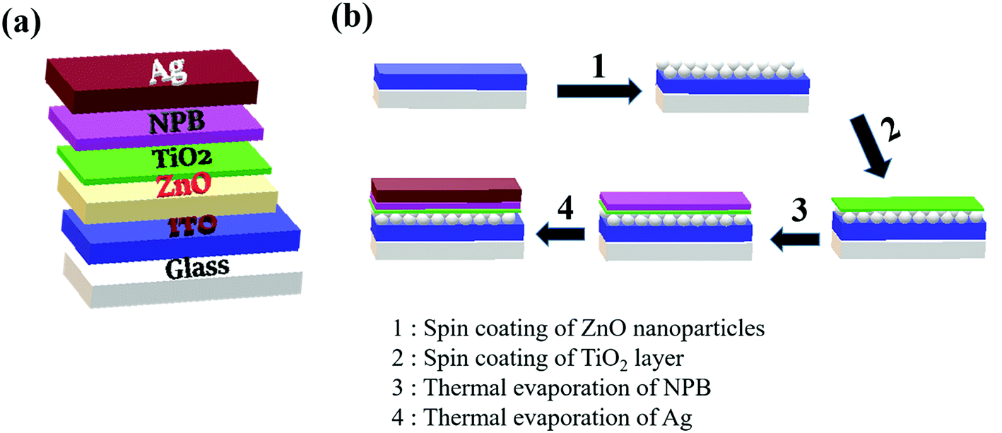 | ||
| Fig. 1 (a) Device structure of the photodetector. (b) Schematic diagram depicting steps of device fabrication. | ||
Characterization of the UV photodetector
The current–voltage characteristics and transient photoresponse of the device were studied with a Keithley 2400 source meter and 6 W ENF 260C Spectroline UV Lamp with 365 nm and 254 nm wavelengths. Spectral response measurements were carried out using a 250 W xenon lamp coupled to a Newport monochromator and chopped at 40 Hz using a light chopper blade as a light source.Results and discussions
Characterization of ZnO
The surface morphology of the annealing-free ZnO thin films was imaged using atomic force microscopy (AFM). Fig. 2 shows the AFM image of a ZnO thin film obtained through tapping mode with 1 μm and 500 nm scanning ranges before and after TiO2 deposition. The nanoparticles were spherical in shape. Thicknesses of the ZnO and TiO2 thin films were determined using profilometry. The RMS surface roughness values of ZnO thin films before and after TiO2 deposition are summarized in the Table 1. The RMS surface roughness of ZnO was low in areas where a compact ZnO layer was formed. However, there were some areas where the depth was higher and this probably led to a greater value for RMS roughness when we selected a large area for the estimation of the same. However, the RMS surface roughness decreased on TiO2 deposition due to the improvement in film quality. The particle size of the ZnO nanoparticles from AFM image was found to be less than 50 nm. The fact that the RMS surface roughness increases only incrementally for longer scan ranges is an indication of the quality and uniformity of the film.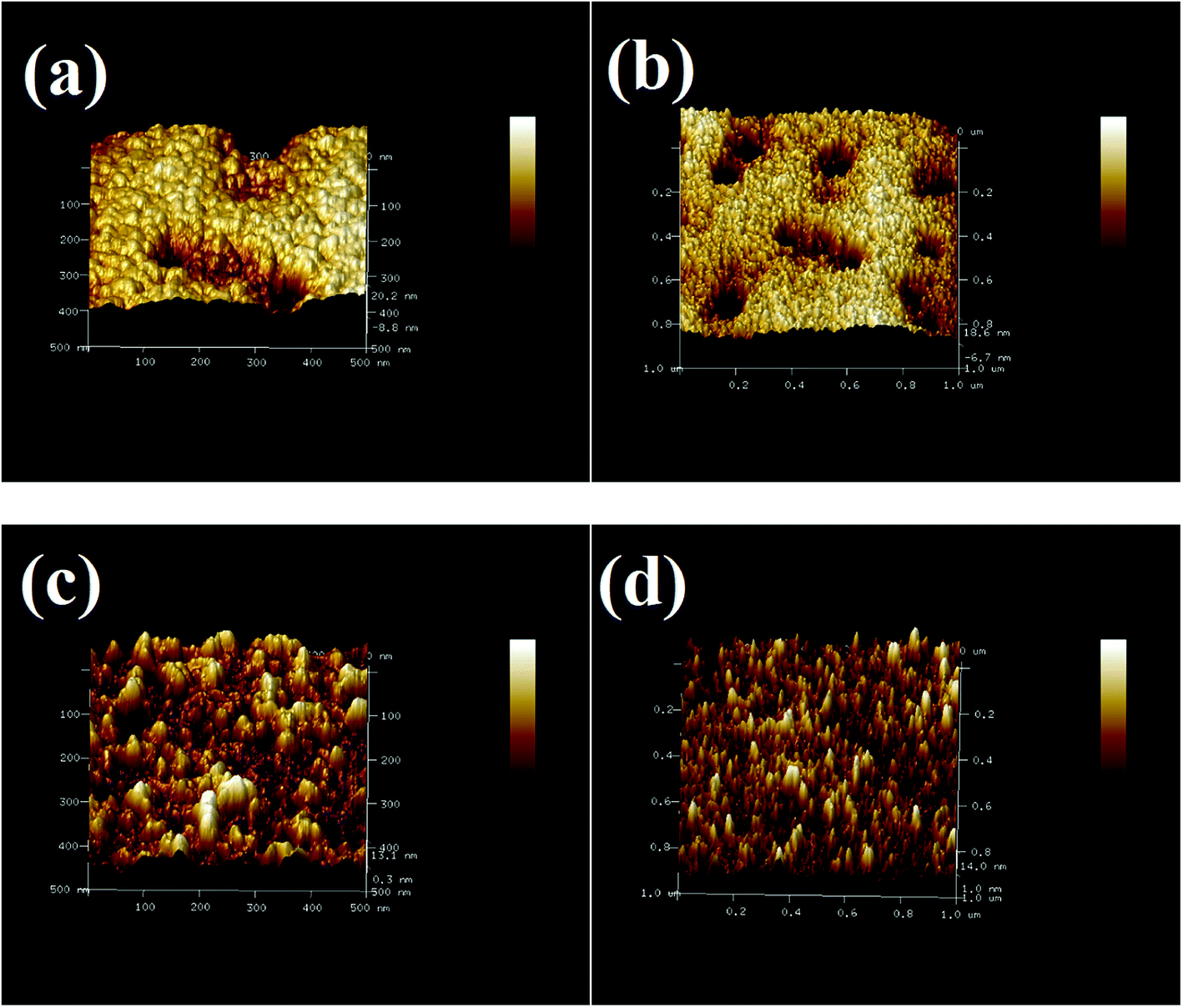 | ||
| Fig. 2 AFM images of annealing-free ZnO thin films before and after TiO2 deposition: (a) and (b) before TiO2 deposition; (c) and (d) after TiO2 deposition. | ||
| Sample | RMS surface roughness (scanning range 500 nm) | RMS surface roughness (scanning range 1 μm) |
|---|---|---|
| ZnO | 6.98 nm | 7.07 nm |
| ZnO + TiO2 | 3.66 nm | 3.71 nm |
The SEM images of the ZnO thin film and synthesized ZnO nanoparticles recorded with a magnification of ×50k are shown in Fig. 3.
 | ||
| Fig. 3 (a) SEM image of annealing-free ZnO thin film. (b) SEM image of synthesized ZnO nanoparticles. | ||
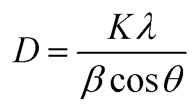
The structural properties of ZnO nanoparticles were studied using XRD and FTIR spectroscopy. The XRD pattern of the ZnO nanoparticles is shown in Fig. 4(a). The (100), (002), (101) (102), (110), (103) and (112) peaks were observed. All the XRD peaks were identified with the standard card JCPDS 36-1451 in the recorded range of 2θ. It was confirmed that the ZnO nanoparticles have a hexagonal wurtzite structure. We calculated the crystallite size for the most intense peak by using Debye Scherrer's formula24
 | (1) |
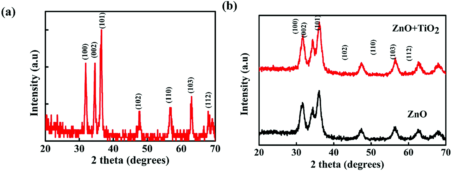 | ||
| Fig. 4 (a) XRD pattern of ZnO nanoparticles. (b) XRD patterns of ZnO thin films before and after TiO2 deposition. | ||
To understand the presence of molecular species in the prepared samples, FTIR studies were conducted within the range from 400 cm−1 to 4000 cm−1 at room temperature. FTIR spectra of ZnO nanoparticles are shown in Fig. 5. Absorption bands below 1000 cm−1 are due to interatomic vibrations of metal oxides.26 The absorption bands observed between 480 cm−1 and 580 cm−1 correspond to the Zn–O stretching mode.27 The n-type conductivity of undoped ZnO is due to the presence of impurities such as hydrogen (H), which is present in almost all growth environments. The interstitial H bonding with oxygen (O) and H substituted for O in ZnO can act as shallow donor levels and contribute to n-type conductivity. Substitutional H is more stable than interstitial H. The peak near 900 cm−1 is related to the hydrogen substituted at the oxygen site bound to the lattice Zn site (i.e., Zn–H).28 The peak near 900 cm−1 is related to the hydrogen substituted at the oxygen site bound to the lattice Zn site (i.e., Zn–H). The IR peaks around 1330 cm−1, 1400 cm−1 and 1570 cm−1 are observed due to symmetric and asymmetric stretching vibrations of C![[double bond, length as m-dash]](https://www.rsc.org/images/entities/char_e001.gif) O group.29 The absorption band near 3400 cm−1 corresponds to the O–H stretching mode.21
O group.29 The absorption band near 3400 cm−1 corresponds to the O–H stretching mode.21
 | ||
| Fig. 5 FTIR spectra of ZnO nanoparticles. | ||
DLS measurements were carried out at 632.8 nm with a He–Ne gas laser at an angle of 175°. The mean diameter of the nanoparticles was 51 nm.
The optical properties of ZnO thin films were studied by using photoluminescence (PL) and UV-visible absorption spectroscopy. The transmittance spectra of ZnO thin film before and after TiO2 deposition are shown in Fig. 6(a). The films yielded transmittance above 85% in the visible region before and after TiO2 deposition, and it can be seen that the transparent nature of ZnO is not affected by TiO2 deposition. This is highly desirable as the transparent nature of ZnO is very important for several optoelectronic applications. The value of the energy band gap of ZnO thin film can be calculated from the Tauc's plot using the relation
| αhν = A(hν − Eg)n | (2) |
| (αhν) = A(hν − Eg)1/2 | (3) |
 | ||
| Fig. 6 (a) Transmittance spectra, (b) Tauc's plot, and (c) Urbach plot of ZnO thin film with and without a TiO2 film. | ||
Fig. 6(b) shows the Tauc's plot of ZnO thin film, and we estimated the band gap to be 3.34 eV. The relation between absorption coefficient and photon energy near the band edge is given by
α = α0![[thin space (1/6-em)]](https://www.rsc.org/images/entities/char_2009.gif) exp(hν/Eu) exp(hν/Eu)
| (4) |
The PL spectra of ZnO thin film excited at 320 nm are shown in Fig. 7. The peak at 370 nm is due to the near band edge emission and the other near 585 nm is due to the oxygen vacancy defect.34 To passivate the defect, a very thin layer of TiO2 is deposited as a surface passivation layer.35 From the PL spectrum of ZnO after TiO2 deposition, it is clear that the intensity of UV emission is enhanced and that of visible emission is suppressed due to decrease in the defect density. The enhancement in UV emission is due to fluorescence resonance energy transfer (FRET) between TiO2 and ZnO thin film, and the reduction in the intensity of the visible emission is due to the surface passivation effect because of the covering by TiO2 layer.35
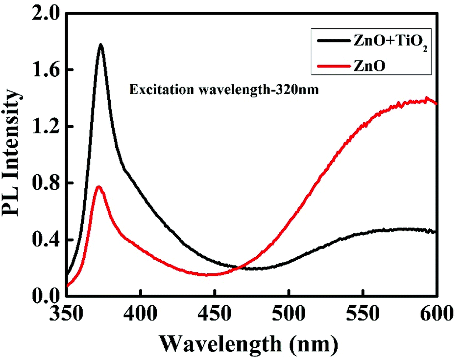 | ||
| Fig. 7 PL spectra of ZnO thin films before and after TiO2 deposition. | ||
Characterization of UV photodetector
The UV radiation spectrum is divided into UV-A (400–320 nm), UV-B (320–280 nm) and UV-C (280–10 nm) regions; UV radiation with wavelength greater than 280 nm can reach the Earth's surface. Overexposure to UV-A and UV-B may result in skin cancer, erythema, premature ageing, burns, etc. UV-C radiation is important for inter-satellite communications. For these reasons, we fabricated a UV photodetector that can detect both UV-A and UV-C radiations. The IV characteristics of the device under dark and 365 nm light illumination at intensity of 1.24 mW cm−2 and 254 nm light illumination at intensity of 2.4 mW cm−2 are shown in Fig. 8(a). Upon UV illumination, ZnO and NPB absorb UV light and generate electron–hole pairs. These electron–hole pairs dissociate into electron and holes by the built-in potential at the organic–inorganic heterojunction. These electrons and holes are collected by the electrodes and thus, a photocurrent is produced. The dark current of the device is 10.2 nA; the photocurrent of the device under 365 nm light illumination is 15 μA and that under 254 nm light illumination is 0.64 μA. The on–off ratio of the device at 365 nm light illumination is 1.5 × 10³ and at 254 nm light illumination, the value is 62. Fig. 8(b) shows the transient photoresponse of the device under 365 nm and 254 nm light illuminations at 0 V with a step size of 10 s. From the transient photoresponse, we calculated a rise time and fall time for the device; the device exhibited a rise time of 156 ms and fall time of 319 ms.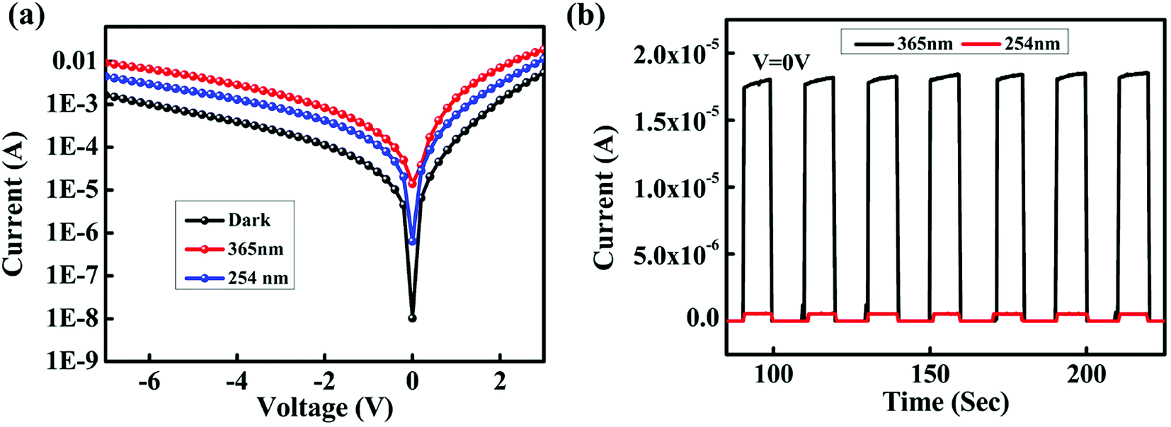 | ||
| Fig. 8 (a) IV characteristics of the photodetector under dark, 365 nm and 254 nm light illumination. (b) Transient photoresponse under 365 nm and 254 nm light illumination at 0 V. | ||
We measured the IV characteristics and transient photoresponse with increasing intensity of illumination at 365 nm. We observed an increase in the photocurrent with an increase in the intensity of illumination. Fig. 9(a) and (b) and show the IV characteristics and transient photoresponse with increase in the intensity of radiation, and Fig. 9(c) shows the transient photoresponse with increasing intensity.
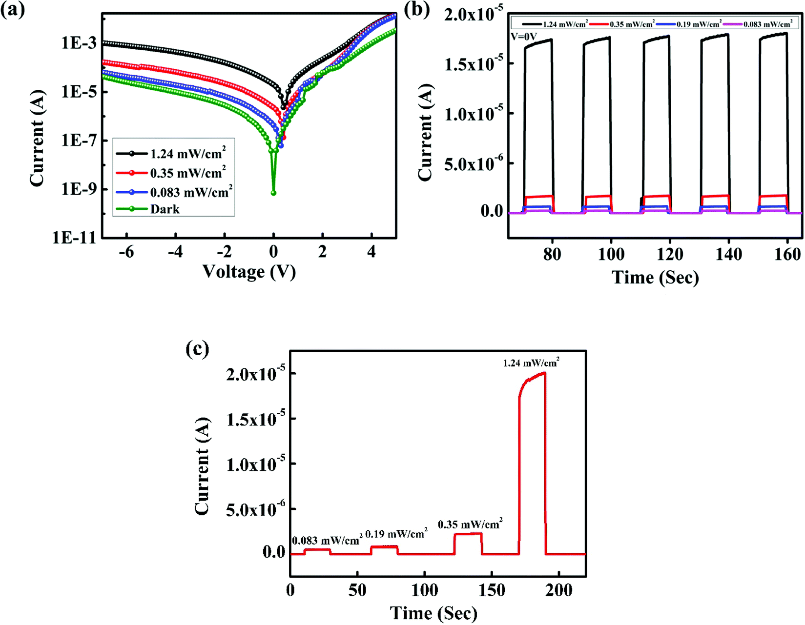 | ||
| Fig. 9 (a) IV characteristics of the photodetector at different UV (365 nm) intensities and (b) transient photoresponses under 365 nm light illumination at different intensities. (c) Transient photoresponse with increasing intensity. | ||
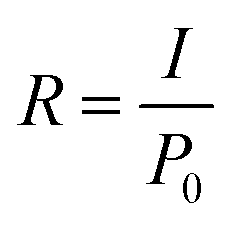
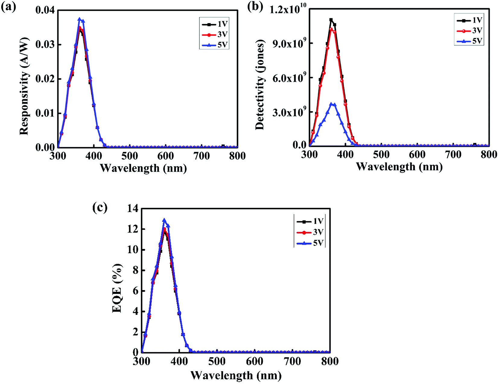
Spectral response measurements were carried out within 300 nm to 800 nm wavelength range using an incident photon to current efficiency (IPCE) measurement system. The spectral response of the device at different bias voltages is shown in Fig. 10(a). From spectral response measurements, it is clear that the device is completely visible-blind and suitable for applications requiring selective UV detection. The maximum response is obtained for 360 nm. The shoulder around 350 nm can be due to absorption by NPB.36 Responsivity is defined as the ratio of the photocurrent to the incident optical power, and it can be calculated using eqn (5):37
 | (5) |
 | ||
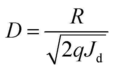
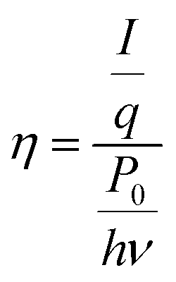
| Fig. 10 (a) Spectral response. (b) Detectivity vs. wavelength. (c) EQE vs. wavelength. | ||
Here, I is the photocurrent and P0 is the incident optical power. We calculated the responsivity at bias values of 1 V, 2 V and 3 V and found that the responsivity increases with an increase in the bias voltage. Detectivity is expressed in the units of jones and is used to characterize the sensitivity of the device. The higher the detectivity, the more sensitive the device will be to a particular wavelength range. From the responsivity, we calculated the detectivity of the device using the relation38
 | (6) |
 | (7) |
 | (8) |
Then, responsivity is calculated as follows:
 | (9) |
This indicates that the responsivity varies with the wavelength λ.39 Fig. 10(c) shows the variation of external quantum efficiency with wavelength. The device exhibited maximum responsivity of 0.037 A W−1 and external quantum efficiency of 12.86% at 360 nm illumination at 5 V. The values of responsivity, detectivity and external quantum efficiency at different bias voltages at 360 nm are summarized in Table 2.
These values are indeed promising when we compare them with recent results for p–n junction-based UV detectors with ZnO. A comparison is given in Table 3.
| Structure | Responsivity (mA W−1) | Detectivity (jones) | On/off ratio | Rise/decay times (ms) | Reference |
|---|---|---|---|---|---|
| p–n junction arrays of ZnO nanofibers | 1 | — | 102 at 2 V | 3900/4710 | 40 |
| Al/PFO/ZnO/ITO | 40 at 2 V | 3 × 10¹⁰ | — | — | 41 |
| ITO/ZnO/PEDOT:PSS/Au | 13 | — | — | 200 | 42 |
| ITO/H:VZnO/PEDOT:PSS/Ag | 2.65 | 5.25 × 10¹⁰ | 23/26 | 43 | |
| ITO/n-ZnO nanorods/i-ZnO/p-GaN | 138.9 | — | 73.3 at −4 V | 1000 | 44 |
| n-ZnO/p-GaN | 450 | — | — | — | 45 |
| n-ZnO/p-NiO/Ni | 2050 | — | 21.3 at −3.5 V | 18100 |
46 |
| ZnO/Sb-doped ZnO nanowire | — | — | 26.5 at −0.1 V | 30 | 47 |
| ITO/NiO/ZnO/Ti/Au | 190 at 1.2 V | 3.8 × 10¹² | — | — | 48 |
| ZnO/PANI | — | — | — | 12000 |
49 |
| p-Si/n-ZnO/Al | 75 | 6.44 × 10⁹ | 1115 at 2 V | — | 50 |
| ITO/ZnO/TiO2/NPB/Ag | 37 | 3.66 × 10⁹ | 103 at 0 V | 156/319 | Present work |
Another important parameter to evaluate the performance of a photodetector is the linear dynamic range (LDR) or the range of current over which the response is linear; it is given by eqn (10), where Imin is the dark current and Imax is the photocurrent.
 | (10) |
LDR of the device is 63 dB. This value is comparable with the LDR value of UV photodetectors fabricated based on InGaAs (66 dB).51 It is very interesting to note that a UV photodetector based on ZnO fabricated from a simple and cost-effective fabrication technique yields an LDR value that is quite similar to that of the one fabricated using energy intensive techniques. We believe that this is an important step in fabricating flexible photodetectors.
Conclusions
We fabricated a low-temperature-processable and visible-blind UV photodetector based on an NPB/ZnO nanoparticle heterojunction, which can work at zero applied bias. The ZnO thin films did not require any annealing and were transparent in the visible region. The device exhibited responsivity of 0.037 A W−1 and EQE of 12.86% at 5 V under 360 nm light illumination. The rise and fall times were 156 ms and 319 ms, respectively. We observed an increase in the photocurrent with increasing intensity of radiation. The results suggest that a UV photodetector with promising performance can be fabricated using annealing-free ZnO films, which may lead to the development of flexible detectors.Conflicts of interest
There are no conflicts to declare.Acknowledgements
One of the authors (H. B.) acknowledges support from University Grants Commission (UGC) of India and N. U. K. N. acknowledges support from DST-AISRF program, Department of Science and Technology, Govt. of India. The authors acknowledge the support from Dr Manoj A. G. Namboothiry, IISER, Thiruvananthapuram for quantum efficiency measurements.References
- L. Sang, M. Liao and M. Sumiya, Sensors, 2013, 13, 10482–10518 CrossRef CAS PubMed.
- K. Liu, M. Sakurai and M. Aono, Sensors, 2010, 10, 8604–8634 CrossRef CAS PubMed.
- Z. Bai, X. Chen, X. Yan, X. Zheng, Z. Kang and Y. Zhang, Phys. Chem. Chem. Phys., 2014, 16, 9525–9529 RSC.
- Y. H. Ko, G. Nagaraju and J. S. Yu, Nanoscale Res. Lett., 2015, 10, 323 CrossRef PubMed.
- L. Qin, C. Shing, S. Sawyer and P. S. Dutta, Opt. Mater., 2011, 33, 359–362 CrossRef CAS.
- Z. Jin, L. Gao, Q. Zhou and J. Wang, Sci. Rep., 2015, 4, 4268 CrossRef PubMed.
- M. Mishra, A. Gundimeda, S. Krishna, N. Aggarwal, L. Goswami, B. Gahtori, B. Bhattacharyya, S. Husale and G. Gupta, ACS Omega, 2018, 3, 2304–2311 CrossRef CAS.
- Y. Xie, L. Wei, G. Wei, Q. Li, D. Wang, Y. Chen, S. Yan, G. Liu, L. Mei and J. Jiao, Nanoscale Res. Lett., 2013, 8, 188 CrossRef PubMed.
- S. Salvatori, M. Rossi, F. Scotti, G. Conte, F. Galluzzi and V. Ralchenko, Diamond Relat. Mater., 2000, 9, 982–986 CrossRef CAS.
- A. Aldalbahi, E. Li, M. Rivera, R. Velazquez, T. Altalhi, X. Peng and P. X. Feng, Sci. Rep., 2016, 6, 23457 CrossRef CAS PubMed.
- V. A. Coleman and C. Jagadish, in Zinc Oxide Bulk, Thin Films and Nanostructures, Elsevier, 2006, pp. 1–20 Search PubMed.
- C. Tian, D. Jiang, B. Li, J. Lin, Y. Zhao, W. Yuan, J. Zhao, Q. Liang, S. Gao, J. Hou and J. Qin, ACS Appl. Mater. Interfaces, 2014, 6, 2162–2166 CrossRef CAS PubMed.
- J. R. D. Retamal, C.-Y. Chen, D.-H. Lien, M. R. S. Huang, C.-A. Lin, C.-P. Liu and J.-H. He, ACS Photonics, 2014, 1, 354–359 CrossRef CAS.
- S. H. Lee, S. Bin Kim, Y. Moon, S. M. Kim, H. J. Jung, M. S. Seo, K. M. Lee, S. Kim and S. W. Lee, ACS Photonics, 2017, 4, 2937–2943 CrossRef CAS.
- B. Guo, G. Wu, H. Chen and M. Wang, Org. Electron., 2016, 29, 13–21 CrossRef CAS.
- J. Ha, S. Yoon, J. Lee and D. S. Chung, Nanotechnology, 2016, 27, 095203 CrossRef PubMed.
- K. S. Ranjith and R. T. Rajendra Kumar, Nanotechnology, 2016, 27, 095304 CrossRef CAS PubMed.
- L.-C. Chen and C.-N. Pan, Eur. Phys. J.: Appl. Phys., 2008, 44, 43–46 CrossRef CAS.
- T. C. Zhang, Y. Guo, Z. X. Mei, C. Z. Gu and X. L. Du, Appl. Phys. Lett., 2009, 94, 113508 CrossRef.
- T. Q. Trung, V. Q. Dang, H.-B. Lee, D.-I. Kim, S. Moon, N.-E. Lee and H. Lee, ACS Appl. Mater. Interfaces, 2017, 9, 35958–35967 CrossRef CAS PubMed.
- M. N. Kamalasanan and S. Chandra, Thin Solid Films, 1996, 288, 112–115 CrossRef CAS.
- L. G. Wang, J. J. Zhu, X. L. Liu and L. F. Cheng, J. Electron. Mater., 2017, 46, 5546–5552 CrossRef CAS.
- S. Alem, J. Lu, R. Movileanu, T. Kololuoma, A. Dadvand and Y. Tao, Org. Electron., 2014, 15, 1035–1042 CrossRef CAS.
- L. Qin, C. Shing and S. Sawyer, IEEE Electron Device Lett., 2011, 32, 51–53 CAS.
- Z. Wang, J. Wang, G. Shi, C. Xu, Z. Hou, Y. Zuo and L. Xi, J. Nanosci. Nanotechnol., 2017, 17, 3829–3834 CrossRef CAS.
- M. I. Khan, K. A. Bhatti, R. Qindeel, N. Alonizan and H. S. Althobaiti, Results Phys., 2017, 7, 651–655 CrossRef.
- R. Kumari, A. Sahai and N. Goswami, Prog. Nat. Sci.: Mater. Int., 2015, 25, 300–309 CrossRef CAS.
- K. Senthilkumar, M. Tokunaga, H. Okamoto, O. Senthilkumar and Y. Fujita, Appl. Phys. Lett., 2010, 97, 091907 CrossRef.
- F. S. Ghoreishi, V. Ahmadi and M. Samadpour, J. Nanostruct., 2014, 3, 453–459 Search PubMed.
- T. K. Pathak, V. Kumar and L. P. Purohit, Physica E Low Dimens. Syst. Nanostruct., 2015, 74, 551–555 CrossRef CAS.
- P. Raghu, C. S. Naveen, J. Shailaja and H. M. Mahesh, in AIP Conference Proceedings, 2016, vol. 1728, p. 020469 Search PubMed.
- Y. Kim and J.-Y. Leem, J. Nanosci. Nanotechnol., 2016, 16, 5186–5189 CrossRef CAS PubMed.
- R. C. Rai, J. Appl. Phys., 2013, 113, 153508 CrossRef.
- A. Gadallah and M. M. El-Nahass, Adv. Condens. Matter Phys., 2013, 2013, 1–11 CrossRef.
- L. Xu, Chin. Opt. Lett., 2009, 7, 953–955 CrossRef CAS.
- Z. Wei, Y. Jun-Sheng, H. Jiang, J. Ya-Dong, Z. Qing and C. Kang-Li, Chin. Phys. B, 2010, 19, 047802 CrossRef.
- R. D. Jansen-van Vuuren, A. Armin, A. K. Pandey, P. L. Burn and P. Meredith, Adv. Mater., 2016, 28, 4766–4802 CrossRef CAS PubMed.
- J. Yu and N. Tian, Phys. Chem. Chem. Phys., 2016, 18, 24129–24133 RSC.
- E. Monroy, F. Omn s and F. Calle, Semicond. Sci. Technol., 2003, 18, R33–R51 CrossRef CAS.
- Y. Ning, Z. Zhang, F. Teng and X. Fang, Small, 2018, 14, 1703754 CrossRef PubMed.
- X. Guo, L. Tang, J. Xiang, R. Ji, K. Zhang, S. K. Lai, J. Zhao, J. Kong and S. P. Lau, AIP Adv., 2016, 6, 055318 CrossRef.
- N. Hernandez-Como, G. Rivas-Montes, F. J. Hernandez-Cuevas, I. Mejia, J. E. Molinar-Solis and M. Aleman, Mater. Sci. Semicond. Process., 2015, 37, 14–18 CrossRef CAS.
- B. Deka Boruah and A. Misra, ACS Appl. Mater. Interfaces, 2016, 8, 18182–18188 CrossRef CAS PubMed.
- L. Zhang, F. Zhao, C. Wang, F. Wang, R. Huang and Q. Li, Electron. Mater. Lett., 2015, 11, 682–686 CrossRef CAS.
- M. Ding, D. Zhao, B. Yao, Z. Li and X. Xu, RSC Adv., 2015, 5, 908–912 RSC.
- Y. H. Ko, G. Nagaraju and J. S. Yu, Nanoscale, 2015, 7, 2735–2742 RSC.
- Y. Wang, Y. Chen, W. Zhao, L. Ding, L. Wen, H. Li, F. Jiang, J. Su, L. Li, N. Liu and Y. Gao, Nano-Micro Lett., 2017, 9, 11 CrossRef.
- M. R. Hasan, T. Xie, S. C. Barron, G. Liu, N. V. Nguyen, A. Motayed, M. V. Rao and R. Debnath, APL Mater., 2015, 3, 106101 CrossRef PubMed.
- H. Wang, G. Yi, X. Zu, P. Qin, M. Tan and H. Luo, Mater. Lett., 2016, 162, 83–86 CrossRef CAS.
- P. Hazra, S. K. Singh and S. Jit, Journal of Semiconductor Technology and Science, 2014, 14, 117–123 CrossRef.
- X. Gong, M. Tong, Y. Xia, W. Cai, J. S. Moon, Y. Cao, G. Yu, C.-L. Shieh, B. Nilsson and A. J. Heeger, Science, 2009, 325, 1665–1667 CrossRef CAS PubMed.
| This journal is © The Royal Society of Chemistry 2018 |