
 Open Access Article
 This Open Access Article is licensed under a Creative Commons Attribution-Non Commercial 3.0 Unported Licence
Reliability enhancement in thin film transistors using Hf and Al co-incorporated ZnO active channels deposited by atomic-layer-deposition†
So-Yeong Na and
Sung-Min Yoon *
*
Department of Advanced Materials Engineering for Information and Electronics, Kyung Hee University, Yongin, Gyeonggi-do 17104, Korea. E-mail: syna95@naver.com; sungmin@khu.ac.kr
First published on 5th October 2018
Abstract
Oxide thin films transistors (TFTs) with Hf and Al co-incorporated ZnO active channels prepared by atomic-layer deposition are presented. The Al concentration was fixed at 2.6 at% and the Hf concentration was varied from 3.3 to 6.3 at%. The HfAlZnO (HAZO) TFTs exhibited positive shifts in turn on voltages toward 0 V with a slight decrease in carrier mobility with increases in the incorporated Hf content and the post-annealing temperature. It was suggested that the carrier concentration and defect densities within the HAZO channels were reduced by incorporating Hf and performing the thermal annealing process. The TFT with HAZO channels with Hf content of 6.3 at% exhibited a turn-on operation at around 0 V and a low SS value of 0.3 V dec−1 without a marked decrease in carrier mobility. Furthermore, the device stabilities under bias, illumination, and temperature stresses could be greatly enhanced by reducing the formation of additional carriers and defects caused by weak Zn–O bonds due to the high binding energy of Hf with oxygen.
1. Introduction
Oxide-based thin-film transistors (TFTs) have actively been researched due to their excellent electrical properties such as good uniformity, high transparency in the visible region, and high field-effect mobility.1,2 By taking these special features, LG Display has released a 65-inch-sized organic light emitting diode (OLED) panel using oxide TFT backplanes for TV applications. Irrespective of this fascinating development in the mass production of OLED TVs, oxide TFTs with higher performance are still required for future display panels with larger areas, faster frame rates, and higher resolution, in which higher carrier mobility, lower operation voltage, and long-term reliability should be achieved at the same time. Especially, the device reliability under illumination and temperature stress conditions applied with bias stress is a key factor requiring much improvement for various practical applications. Moreover, it is desirable for the turn-on operation to be activated around 0 V in terms of reducing power consumption.To achieve the production of more enhanced oxide TFTs, there are lots of factors affecting the device characteristics of oxide TFTs, such as fabrication process conditions including post-annealing temperatures,3,4 device structures,5,6 gate insulators,7,8 and semiconducting active compositions.9–11 Among them, the material design of the active channel can be a powerful method to effectively control the device properties. The ZnO-based oxide semiconductors have attracted much attention as active layers for TFTs due to their specific features such as wide bandgaps, high transmittance in the visible region, and low-temperature process compatibility.12–16 Recently, there have been numerous works on the introduction of various metal atoms into ZnO,17–19 which should be considered for the appropriate regulation of the carrier concentration for achieving robust stability and a low operation voltage. Hf or Al, with higher oxygen binding energies compared with Zn, can act as effective carrier suppressors for ZnO TFTs. The oxygen binding energies of Hf, Al, and Zn are 791, 512, and 284 kJ mol−1, respectively. Therefore, the turn-on voltage (Von) shifts under bias and temperature stresses can be reduced by incorporating the stability enhancer Hf, by suppressing oxygen vacancy formation.20 Alternatively, the electrical conductivity of Al-doped ZnO films can be controlled by changing the Al content within the ZnO,21 and hence, the Al can act as a conductivity modulator (Fig. S1†). In this light, Hf and Al co-incorporated ZnO can be employed as a prospective channel material in terms of obtaining both the properties of stability enhancement in TFT operations and conductivity control in ZnO channel layers.
The film deposition method is another crucial point. As devices are scaled down, the device structures become more complicated in order to have high aspect ratio. Even though sputtering was conventionally used for preparing oxide semiconductor channels such as InGaZnO (IGZO),22,23 it is not suitable for forming conformal films on specific regions of scaled down devices over large areas. Solution coating processes can be suggested as alternative methods, but the device performances are not appropriate for mass production owing to difficulties in guaranteeing process uniformity and reproducibility. Besides, the film composition is also one of the most important parameters to be carefully adjusted. From this viewpoint, atomic layer deposition (ALD) has been recently introduced to form functional oxide semiconductors.24–26 This could be one of the best solutions for preparing HfAlZnO (HAZO) active channels to figure out the effects of Hf and Al incorporation on the characteristics of the HAZO TFT. Furthermore, ALD can be used as an exclusive method to form functional oxide thin films at the atomic level by designing the precursor pulse and purge sequences. The ALD method guarantees that the active channel layer can have a homogenous and smooth surface with good interfaces between HAZO active and Al2O3 gate insulator layers. Especially, the film composition can be easily modulated by simply controlling the number of inserted cycles and combining several different precursors.
Thus, in this work, we fabricated top-gate transparent oxide TFTs using the first proposed HAZO active channels using ALD. The effects of Hf and Al co-incorporation and the post annealing process on the device performance were extensively investigated. By suitably controlling the Hf concentration, highly stable characteristics under illumination and temperature stress, as well as good transfer characteristics including Von near 0 V could be obtained. The origins of the variations in TFT characteristics and instabilities of our proposed HAZO TFTs were thoroughly discussed to understand the device operations depending on the incorporated Hf content.
2. Experimental
Fig. 1a shows a cross-sectional diagram of the top-gate HAZO TFT fabricated on a glass substrate. Firstly, 150 nm-thick indium-tin-oxide (ITO) layers were patterned into source/drain (S/D) electrodes. The HAZO thin films (13 nm) were deposited as active channel layers via ALD at 100 °C followed by the successive deposition of a 9 nm-thick Al2O3 protection layer (PL) at 150 °C. Tetrakis(ethylmethylamino)hafnium (TEMAHf), trimethylaluminium (TMA), diethylzinc (DEZ), and water vapor (H2O) were used as Hf, Al, and Zn precursors and an oxidant, respectively. Even though it has been reported that ozone (O3) as an oxidant may enhance the reactivity of each metal precursor and reduce the defect states within the oxide thin films,27,28 the combination of TEMAHf, TMA, DEZ, and H2O has no limitations for preparing HAZO active channels for TFT applications. Thus, in this work, H2O was chosen as the oxygen precursor for the deposition of HAZO thin films. The TEMAHf and TMA pulses were incorporated between DEZ pulses to control the HAZO film composition. The number of cycles composed of TMA and H2O, which determines the amount of incorporated Al, was varied from 2 to 4. However, sound device characteristics could not be obtained for the HAZO channels prepared by 4-cycles of Al incorporation, as shown in the ESI (Fig. S1†). Therefore, the number of cycles of Al incorporation was fixed at 2, in this study. To investigate the effects of variations in the amount of incorporated Hf, the number of cycles composed of TEMAHf and H2O pulses was varied to 4, 6, 8, and 10 over a total of 100 cycles. For convenience, the devices using HAZO channels with different Hf amounts were termed as H4, H6, H8, and H10, respectively. The detailed cycle configurations are illustrated in Fig. 1b. Then, the HAZO and PL were simultaneously patterned using a diluted hydrofluoric acid-based (DHF) wet etchant. Next, Al2O3 gate insulators (GIs) were formed by ALD at 150 °C and etched with phosphoric acid to form contact holes. 150 nm-thick ITO films were deposited via a DC sputtering method and patterned into gate electrodes and S/D pads by a lift-off process.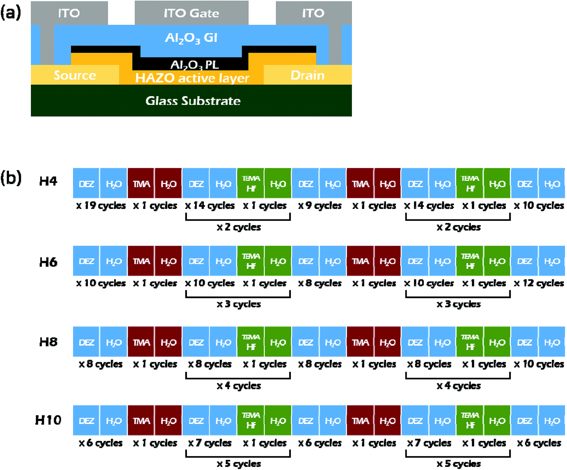 | ||
| Fig. 1 (a) Schematic cross-sectional view of the fabricated HAZO TFTs. (b) ALD cycle configurations for the HAZO thin films employed as active layers for H4, H6, H8, and H10, respectively. | ||
The variations in composition and bonding characteristics of the ALD-grown HAZO films were analyzed using X-ray photoelectron spectroscopy (XPS) to investigate the effect of variations in the content of incorporated Hf. The electrical conductivities (σc) of the HAZO thin films with different Hf concentrations were examined using in situ four-point probe measurements. The surface morphologies and film crystallinities of the HAZO thin films were examined using atomic force microscopy (AFM) and X-ray diffraction (XRD). The device characteristics of the fabricated HAZO TFTs were evaluated using a semiconductor parameter analyzer (Keithley 4200SCS) in a dark box at room temperature (RT). The channel width (W) and length (L) of the evaluated TFTs were 40 and 20 μm, respectively. The device characteristics including the IDS scalability of the fabricated HAZO TFTs were also well confirmed even when the channel areas of the devices were changed.
3. Results and discussion
Fig. 2 shows the variation in the film composition of the HAZO thin films when the number of ALD cycles for Hf incorporation was controlled to be 4, 6, 8, and 10, respectively. The atomic ratio of Al was approximately 0.026 for all of the films. The atomic ratios of Hf/Zn were 0.033/0.436, 0.040/0.411, 0.053/0.391, and 0.063/0.372 as the cycle number of Hf changed to 4, 6, 8, and 10, respectively. The Hf incorporation ratio increased with an increase in the number of ALD cycles with TEMAHf. It can be suggested from the results that the film compositions could be well modulated by controlling the ALD cycle configurations. | ||
| Fig. 2 Variations in atomic ratios of the HAZO thin films prepared by ALD as a function of the TEMAHf cycle number inserted into the full cycle configurations. | ||
To investigate the temperature-dependent electronic properties of the HAZO thin films prepared by ALD, variations in sheet resistance (Rs) were measured using in situ four-point probe measurements. The Rs values of each film with different Hf concentrations were measured when the temperature was changed from 50 to 300 °C in both forward and reverse directions, and the ramping rate was fixed at 5 °C min. The σc values were calculated using Rs values, as shown in Fig. 3. The initial values of σc were approximately 10−10 S cm−1 for all the films, indicating almost insulating properties, which means that the carriers were not activated for transport conduction. However, when the temperature reached specific values, which were estimated to be 123, 135, 143, and 155 °C for the HAZO films prepared by Hf incorporation cycle numbers of 4, 6, 8, and 10, respectively, the σc values started to increase remarkably. From these results, it can be suggested that the HAZO thin films have typical semiconducting properties irrespective of the amount of incorporated Hf. Furthermore, the HAZO films with higher Hf contents required more thermal energy to initiate carrier transport for electrical conduction, which was related to the reduction of conduction carriers such as oxygen vacancies with increased incorporation of Hf due to the high binding energy of Hf with oxygen. To investigate the obtained measurement data in more detail, we calculated the activation energies (EA) for carrier transport by using the Arrhenius equation described in eqn (1).
 | (1) |
 | ||
| Fig. 3 Variations in the temperature-dependent electrical conductivities of the ALD-grown HAZO thin films with different Hf concentrations. | ||
For further analysis on the temperature-dependent σc values and the EA values for the electron transport, the temperature range was classified into two regions. In region 1 (i.e. x > 2.5), the EA values were examined to compare the electronic natures of the HAZO films with different Hf contents right after the critical temperatures. The calculated EA values were obtained as 3.52, 3.42, 3.35, and 3.48 eV for the HAZO films prepared with Hf incorporation cycle numbers of 4, 6, 8, and 10, respectively. Considering that the EA values represent the energy quantities required for activating the conduction carriers, there were no marked differences in the origins of the carrier transport in this region among the HAZO films with various amounts of incorporated Hf, once the transport conduction was initiated. Alternatively, in region 2 defined as higher temperature, the σc values of each film with different Hf concentrations started to exhibit different behaviors. There were no marked differences in EA values for the devices without H10, which were estimated to be 4.13, 4.20 and 4.19 eV for the compositions of H4, H6, and H8, respectively. On the contrary, the H10 did not show any changes in σc even when the temperature was 300 °C in region 2. It is noteworthy that there were meaningful variations in the final σc values obtained in region 2 among the HAZO films. When the incorporated Hf cycle number was varied from 8 to 4, the final σc values of the HAZO thin films showed an increasing trend. The higher σc value of the HAZO film with a lower Hf content could result from a larger quantity of defect-assisted conduction carriers within the film. In other words, the defect-assisted conduction carrier concentration can be supposed to decrease with increased incorporation of Hf within the ALD-prepared HAZO film. Consequently, it was suggested that the electronic characteristics of the HAZO thin films could be controlled by changing the ALD cycle configurations of the Hf precursors.
Physical properties of surface morphology and crystallinity of the HAZO thin films with different Hf contents were also investigated using atomic force microscopy and X-ray diffraction analysis. All the films showed uniform and smooth surfaces, as shown in Fig. S2.† Moreover, the HAZO thin films were confirmed to have amorphous phases even after heat treatment performed at 600 °C, as shown in Fig. S3.†
Based on the above-mentioned physical properties and composition controllability of the ALD-grown HAZO thin films, the HAZO TFTs were fabricated with different Hf contents from 3.3 to 6.3 at% and the device characteristics were compared among the devices to examine the effects of Hf incorporation into the Al-doped ZnO active channels. Fig. 4a shows the IDS–VGS transfer curves of the HAZO TFTs depending on the Hf concentration. The VGS was swept from −25 to 25 V in forward and reverse directions and the VDS was set as 10.5 V. The carrier mobilities at saturation (μsat) regions were obtained as 0.41, 0.59, 0.63, and 0.70 cm2 V−1 s−1 for the H4, H6, H8, and H10 devices, respectively. Alternatively, the linear mobilities (μlin) were calculated as 2.20, 1.58, 1.30, and 1.21 cm2 V −1 s−1 for H4, H6, H8, and H10, respectively. Even though the μsat and μlin values showed clear increasing and decreasing trends, respectively, with increased amounts of incorporated Hf, there were not such marked differences among the devices. These small variations among the devices were supposed to result from the minutely modulated electronic natures of the HAZO channels with different Hf contents, as observed in Fig. 2 and 3. Besides, all the devices showed low SS values of approximately 300 mV dec−1. Table 1 summarizes the device parameters including μlin, μsat, SS, and the threshold voltage (VTH) of each device. In contrast, the location of Von evidently shifted in a positive direction toward 0 V with an increase in the incorporated Hf amount due to the reduction in the number of carriers. However, even for H10, the Von still existed at a VGS of less than −5 V. It is well known that a post-annealing process in ambient O2 can be a good remedy for controlling the Von near 0 V due to the reduction of oxygen vacancies and conduction carriers in metal oxide semiconductors.29 Thus, to investigate the effects of thermal treatments, the fabricated HAZO TFTs were post-annealed in an O2 atmosphere. Fig. 4b shows the IDS–VGS curves of H10 when post-annealing processes were performed at 150, 180, and 200 °C in ambient O2 for 1 h after device fabrication. It is noteworthy that the H10 device turned on at almost 0 V after annealing at 150 °C. The carrier mobility and on-current slightly decreased when the annealing temperature was increased from 150 to 200 °C, which resulted from the filling the oxygen vacancies with ambient oxygen atoms.30 To sum up, the number of carriers and defects such as oxygen vacancies in the HAZO thin films could be reduced with an increase in cycles of Hf insertion during the ALD process and thermal annealing. However, in terms of transfer characteristics, the reduction of carriers was dominantly influential on the characteristics of the HAZO TFTs, showing a slight decrease in carrier mobility and positive shifts of Von. Consequently, it was concluded that the Von characteristics of the HAZO TFTs could be well modulated without marked decrease of the carrier mobility by effectively controlling the carrier concentration within the channel, which was achieved by Hf and Al co-incorporation and a suitable post-annealing process.
 | ||
| Fig. 4 (a) Comparisons of IDS–VGS characteristics and IGS leakage components of the fabricated devices with different Hf concentrations. (b) Variations in IDS–VGS characteristics and IGS leakage components of the H10 device depending on the post-annealing temperature. | ||
| Device H4 | Device H6 | Device H8 | Device H10 | |
|---|---|---|---|---|
| VTH [V] | −14.24 | −2.97 | 2.22 | 2.94 |
| Von [V] | −19.0 | −14.4 | −9.0 | −5.8 |
| Ion [μA] | 32 | 17 | 8.8 | 11 |
| μlin [cm2 V−1 s−1] | 2.20 | 1.58 | 1.30 | 1.21 |
| μsat [cm2 V−1 s−1] | 0.41 | 0.59 | 0.63 | 0.70 |
| SS [V dec−1] | 0.24 | 0.29 | 0.36 | 0.34 |
As can be seen in Fig. 4, even though there were significant variations in VTH (Von) among the fabricated HAZO TFTs, the incorporated Hf amount did not have any crucial impacts on the device performances such as carrier mobility and SS values. The device reliability is also one of the most important specifications to be carefully considered in TFT characteristics. Thus, the device operations of the HAZO TFTs were compared under bias, temperature, and illumination stress conditions. Fig. 5a–c show the variations in transfer characteristics under positive bias stress (PBS) for H6, H8, and H10, respectively. A VGS of 20 V was continuously applied for 10![[thin space (1/6-em)]](https://www.rsc.org/images/entities/char_2009.gif) 000 s and the VDS was fixed at 10.5 V at RT during the test. The threshold voltage shifts (ΔVTH) of H6, H8, and H10 were estimated to be −0.24, −0.19, and +0.18 V, respectively. It is encouraging that all of the devices showed small ΔVTH of less than ±0.3 V. Furthermore, the ΔVTH could be reduced by increasing the Hf contents. The direction of ΔVTH is an important issue to be extensively discussed. Generally, the VTH moves in a positive direction under PBS conditions due to electron trapping. However, for H6 and H8 using HAZO channels with Hf contents less than 6 at% (confirmed by XPS), the VTH was negatively shifted under PBS. These anomalous ΔVTH values were suggested to originate from the composition differences in the HAZO active channels among the devices.31 There are relatively weak Zn–O bonds in the HAZO films due to low bonding energy between the Zn and oxygen. These weakly-bonded metal ions capture electrons under positive gate bias. The bonding force with oxygen anions will be temporarily lowered and the bonds can be broken. As a result, the transfer curves shift in a negative direction owing to the increase in conduction carriers released from broken bonds. Consequently, the negative ΔVTH under PBS was suggested to be mainly caused by weak Zn–O bonds within the HAZO channels, although the electron trapping basically works in H6 and H8. The negative ΔVTH decreased with an increase in incorporated Hf contents owing to the higher bond energy of Hf–O compared with Zn–O. Alternatively, for H10 when the Hf contents approached 6 at%, which was enough to prevent carrier formation under PBS, the ΔVTH showed a positive value. In other words, the additional carrier formation resulting from the weak Zn–O bonds could be effectively suppressed by increasing the incorporated Hf amount. As a result, the incorporated Hf could greatly improve the PBS stability of the fabricated HAZO TFT.
000 s and the VDS was fixed at 10.5 V at RT during the test. The threshold voltage shifts (ΔVTH) of H6, H8, and H10 were estimated to be −0.24, −0.19, and +0.18 V, respectively. It is encouraging that all of the devices showed small ΔVTH of less than ±0.3 V. Furthermore, the ΔVTH could be reduced by increasing the Hf contents. The direction of ΔVTH is an important issue to be extensively discussed. Generally, the VTH moves in a positive direction under PBS conditions due to electron trapping. However, for H6 and H8 using HAZO channels with Hf contents less than 6 at% (confirmed by XPS), the VTH was negatively shifted under PBS. These anomalous ΔVTH values were suggested to originate from the composition differences in the HAZO active channels among the devices.31 There are relatively weak Zn–O bonds in the HAZO films due to low bonding energy between the Zn and oxygen. These weakly-bonded metal ions capture electrons under positive gate bias. The bonding force with oxygen anions will be temporarily lowered and the bonds can be broken. As a result, the transfer curves shift in a negative direction owing to the increase in conduction carriers released from broken bonds. Consequently, the negative ΔVTH under PBS was suggested to be mainly caused by weak Zn–O bonds within the HAZO channels, although the electron trapping basically works in H6 and H8. The negative ΔVTH decreased with an increase in incorporated Hf contents owing to the higher bond energy of Hf–O compared with Zn–O. Alternatively, for H10 when the Hf contents approached 6 at%, which was enough to prevent carrier formation under PBS, the ΔVTH showed a positive value. In other words, the additional carrier formation resulting from the weak Zn–O bonds could be effectively suppressed by increasing the incorporated Hf amount. As a result, the incorporated Hf could greatly improve the PBS stability of the fabricated HAZO TFT.
 | ||
| Fig. 5 Variations in the IDS–VGS curves under PBS conditions of the HAZO TFTs at a VGS of 20 V when the Hf cycle numbers were (a) 6, (b) 8, and (c) 10, respectively. | ||
For liquid-crystal display backplane device applications, a negative bias is constantly applied to completely turn-off the TFTs while the back-light is on. Therefore, the TFTs should operate in a stable manner, showing no change in Von, even when negative bias and illumination stresses are simultaneously applied. Because of this, the ΔVTH in the IDS–VGS characteristics were examined under negative bias illumination stress (NBIS) conditions. Fig. 6a–c show the variations in transfer characteristics under NBIS for H6, H8, and H10, respectively, in which a white light emitting diode was used with an irradiation intensity of 0.1 mW cm−2. A VGS of −20 V was continuously applied and the VDS was fixed at 10.5 V. After 10000 s of negative bias stress with wavelengths in the white region, ΔVTH values were −3.6, −2.4, and −1.6 V for H6, H8, and H10, respectively. All the devices showed negative ΔVTH without significant decreases in the carrier mobilities and SS. Furthermore, the ΔVTH showed a decreasing trend with an increase in the contents of incorporated Hf. To figure out the origins for the NBIS instabilities among the devices employing the HAZO channels with different Hf contents, the variations of the ΔVTH values during the NBIS tests for each device were fitted with a stretched exponential equation as described in eqn (2)32,33 as a function of stress time, as shown in Fig. 6d.
| ΔVTH = ΔVTH0{1 − exp[−(t/τ)β]} | (2) |
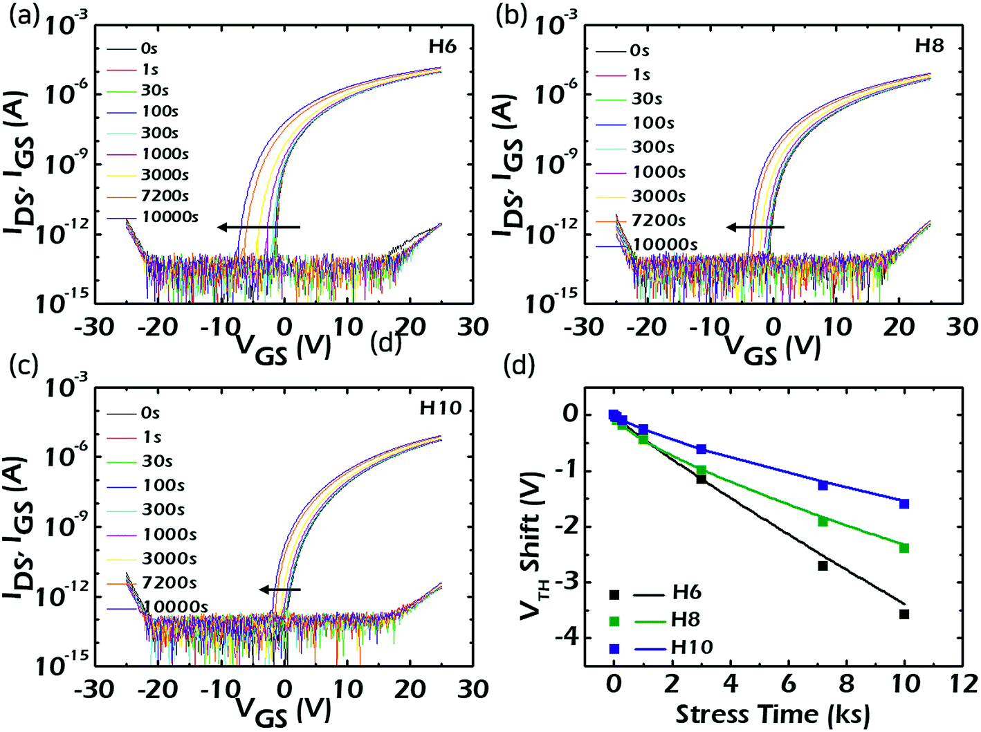 | ||
| Fig. 6 Variations in the IDS–VGS curves under NBIS conditions of the HAZO TFTs at a VGS of −20 V with wavelengths in the white region, when the Hf cycle numbers were (a) 6, (b) 8, and (c) 10, respectively. (d) Variations of the ΔVTH values of each device under NBIS tests as a function of stress time. | ||
In this equation, ΔVTH0 corresponds to the ΔVTH at infinite time, which corresponds to the difference between the gate bias stress and the initial threshold voltage, β is the stretched-exponential exponent, and τ is the characteristic trapping time of carriers. The calculated β and τ values for each device are summarized in Table 2.
| β | τ | |
|---|---|---|
| Device H6 | 0.92 | 1.00 × 10⁵ |
| Device H8 | 0.72 | 3.74 × 10⁵ |
| Device H10 | 0.78 | 5.21 × 10⁵ |
As can be seen in Fig. 6d, the ΔVTH variations for H6, H8, and H10 were quite well fitted with the equation. The τ values indicate how easily carriers generated by NBIS can be injected into the GIs or near the active/GI interfaces. It is noteworthy that the τ values showed an increasing trend with an increase in the Hf contents. In other words, when the incorporated Hf amount increases in the HAZO channel, the generated positive holes require a longer time to be trapped under the NBIS conditions. Therefore, it was found from these results that hole trapping within the GIs or at the interfaces between the HAZO channel and the GIs was considered as the main origin for the VTH shift induced by NBIS. It was also suggested that the charge trapping phenomenon could be effectively suppressed when the Hf contents within the HAZO were increased from 4.0 to 6.3 at%. Especially, for the H10 device, the device stability under NBIS was greatly enhanced, showing a ΔVTH as small as −1.6 V. These obtained NBIS stabilities of our proposed HAZO TFTs are far superior results compared with those of previously reported oxide TFTs.34,35
The positive bias temperature stress (PBTS) and negative bias temperature stress (NBTS) stabilities were also examined for verifying long-term stability at high temperature. The NBTS stabilities were verified well for the fabricated devices, as shown in the ESI (Fig. S4†). In addition, the PBTS stabilities were investigated at temperatures of 40 and 80 °C. The PBTS characteristics obtained at 40 °C showed a similar trend to those examined under PBS at RT (20 °C). The ΔVTH values during the PBTS tests were estimated as −0.72, 0.29, and 1.87 V for H6, H8, and H10, respectively, without marked decreases in the values of carrier mobility and SS. It was found from these results that the amount of negative shift in VTH decreased with an increase in the incorporated Hf contents owing to the higher bonding energy of Hf–O compared with Zn–O, even though the H8 showed a slightly positive ΔVTH in contrast with the PBS test. Thus, in order to clearly investigate the PBTS instabilities of the HAZO TFTs fabricated by preparing HAZO channels with different amounts of incorporated Hf, the measurement temperature was chosen to be a higher temperature of 80 °C. Fig. 7a–c show the variations in transfer characteristics under PBTS for H6, H8, and H10, respectively. The devices were stressed under a VGS of 20 V and the VDS was fixed at 10.5 V while keeping the substrate temperature at 80 °C for 10000 s. Unlike the cases of the PBS and NBIS tests, it was noticeable that the transfer characteristics experienced variations in carrier mobility and SS values as well as the ΔVTH under the PBTS conditions. Thus, there were some discrepancies in behaviors between the ΔVon and ΔVTH among the evaluated devices. While H6 and H8 exhibited negative ΔVon under PBTS, which were estimated as −3.9 and −3.6 V, respectively, the H10, with the HAZO channels with incorporated Hf amounts larger than 6 at%, showed a positive shift of Von of 0.4 V. Alternatively, the VTH values calculated for all of the devices moved in a positive direction as a function of stress time. These discrepancies between ΔVon and ΔVTH resulted from the decrease in mobility of the HAZO TFTs during the PBTS tests. In other words, the PBTS instabilities cannot be simply explained by the sole mechanism of electron trapping and multiple origins can be involved in the behaviors of the devices under PBTS. Two types of feasible scenarios can be suggested as follows: (1) electron trapping can be a basic origin for the ΔVon and ΔVTH under PBTS. Actually, the VTH values of all the devices were positively shifted as a function of stress time and their variations obeyed the stretched exponential equation only in specified time domains, which corresponded to approximately 1000, 1000, and 7200 s for H6, H8, and H10, respectively, as can be seen with the solid lines in Fig. 7d. However, they showed negative ΔVTH after the specified points of stress time and their variations did not precisely obey the stretched exponential relationship due to the effects of decreased mobility. The degree of deviations in the measured ΔVTH values from the calculated values decreased with an increase in the content of incorporated Hf. Moreover, the ΔVTH showed an increasing trend as the incorporated Hf content increased, even though the ΔVon was markedly reduced with an increase in the Hf content. Concerning these problems, the second origin should be additionally discussed. (2) As mentioned above, the relatively weak bonds of Zn–O within the HAZO thin film can play major roles in influencing the device stability, which can be classified in two ways under the PBTS conditions. Firstly, the weakly-bonded Zn–O can generate conduction carriers, which is similar to the situation under PBS. The Zn ions with weak bonds capture electrons under positive bias and the conduction carriers released from the broken Zn bonds induce the negative ΔVon. Secondly, the weakly-bonded Zn–O can also work as a donor-like state under the conduction band minimum of the HAZO.36,37 The carrier mobility may be decreased by these donor-like defects, especially when positive bias is applied at high temperatures. A number of defect sites can be more easily generated at higher temperatures. Therefore, the decrease of mobility was additionally involved in device instabilities under PBTS compared with those under PBS. Consequently, the PBTS instabilities of the evaluated devices were influenced by both the effects of the negative ΔVon in the subthreshold region, which resulted from additional carrier formation within the channel, and the decrease of mobility caused by the donor-like defects generated at high temperatures.
 | ||
| Fig. 7 Variations in IDS–VGS curves under PBTS conditions of the HAZO TFTs at a VGS of 20 V with a substrate temperature of 80 °C when the number of Hf cycles were (a) 6, (b) 8, and (c) 10, respectively. (d) Variations in the ΔVTH values for H6, H8, and H10 as a function of PBTS time. | ||
Here, it would be interesting to discuss the composition dependence on the PBTS instabilities. H6 and H8 with HAZO channels with Hf contents less than 6 at% experienced the complex origins of electron trapping, conduction carrier generation, and donor-like defect creation under PBTS. However, the carrier generation and decrease in mobility were dominantly activated owing to the larger number of weak Zn–O bonds, and hence the Von was negatively shifted during the PBTS tests. Conversely, when the incorporated Hf contents were larger than 6 at%, positive ΔVon was detected with a small decrease in mobility under PBTS due to mixed mechanisms of electron trapping and donor-like defect generation. In other words, the additional carrier formation and defect sites caused by weakly-bonded Zn–O could be suppressed for H10 due to the higher bonding energy of Hf ions with oxygen. Furthermore, the degree of the decrease of mobility for H10 was remarkably smaller than those for H6 and H8. The carrier mobility variations during PBTS from the initial values were estimated to be 17.1, 15.0, 6.1% for the H6, H8, and H10, respectively. Therefore, in the case of PBTS, ΔVon could be compromised to be nearly 0 V with a small degree of decrease in mobility with an incorporated Hf concentration larger than 6 at% (H10). Consequently, the PBTS stabilities of the proposed HAZO TFTs could be sensitively modulated and improved by incorporating optimum amounts of Hf.
4. Conclusions
We investigated the physical and electrical properties of Hf and Al co-incorporated ZnO thin films for the active channels of TFTs. The HAZO thin films were prepared by ALD, and were designed to examine the effects of the amount of incorporated Hf on the device characteristics. The Al composition was fixed at 2.6 at% and the Hf concentration were varied from 3.3 to 6.3 at% by controlling the ALD cycle configuration. The ALD HAZO thin films showed uniform and smooth surfaces showing low Ra values of approximately 0.5 nm and amorphous phases were observed for all the HAZO compositions with different amounts of Hf incorporation. The electronic natures of the HAZO thin films were well modulated by adjusting the Hf contents. The carrier concentration and amount of defect sites decreased with an increase in the contents of incorporated Hf. From these results, we confirmed that the HAZO thin films can be utilized as active layers for oxide TFTs.Then, we fabricated TFTs using the HAZO channels with different Hf concentrations. The HAZO TFT with Hf content of 6.3 at% showed good characteristics such as a low SS value of 0.3 V dec−1 and an appropriate Von controlled at around 0 V with a moderate value of carrier mobility, which was suggested to originate from the controlled carrier concentration and defect densities within the HAZO channels due to suitable amounts of Hf incorporation. Although the carrier mobility was slightly decreased as the incorporated Hf contents were increased, the long-term stabilities were greatly enhanced under bias, illumination, and temperature stresses owing to the higher bonding energy of Hf with oxygen atoms. As a result, highly-stable TFTs operated at lower voltage could be obtained by employing HAZO channels controlled by optimum ALD conditions and a suitable post-annealing process. In conclusion, our proposed HAZO channels prepared by an ALD process can be a useful material for enhancing device reliabilities and to provide backplane devices with robust stabilities for future applications in the display industry.
Conflicts of interest
There are no conflicts of interest to declare.Acknowledgements
This work was partly supported by the Korea Evaluation Institute of Industrial Technology through the Korean Government (10079974, Development of core technologies on materials, devices, and processes for TFT backplane and light emitting frontplane with enhanced stretchability above 20%, with application to stretchable display), and by the Kyung Hee University–Samsung Electronics Research and Development Program entitled Flexible Flash Memory Device Technologies for Next-Gen Consumer Electronics.References
- E. Fortunato, P. Barquinha and R. Martins, Adv. Mater., 2012, 24, 2945–2986 CrossRef CAS PubMed.
- S. J. Kim, S. H. Yoon and H. J. Kim, Jpn. J. Appl. Phys., 2014, 53, 02BA02 CrossRef.
- J. S. Park, J. K. Jeong, Y. G. Mo, H. D. Kim and S. I. Kim, Appl. Phys. Lett., 2007, 90, 262106 CrossRef.
- M. Miyakawa, M. Nakata, H. Tsuji, Y. Fujisaki and T. Yamamoto, AIP Adv., 2016, 6, 085016 CrossRef.
- M. K. Ryu, S. H. Ko Park, C. S. Hwang and S. M. Yoon, Solid-State Electron., 2013, 89, 171–176 CrossRef CAS.
- C. H. Ahn, M. G. Yun, S. Y. Lee and H. K. Cho, IEEE Trans. Electron Devices, 2014, 61, 73–78 CAS.
- S. Y. Na, Y. M. Kim, D. J. Yoon and S. M. Yoon, J. Phys. D: Appl. Phys., 2017, 50, 495109 CrossRef.
- I. K. Lee, S. W. Lee, J. G. Gu, K. S. Kim and W. J. Cho, Jpn. J. Appl. Phys., 2013, 52, 06GE05 CrossRef.
- J. Y. Bak, S. H. Yang and S. M. Yoon, Ceram. Int., 2013, 39, 2561–2566 CrossRef CAS.
- S. H. Oh, B. S. Yang, Y. J. Kim, M. S. Oh, M. Jang, H. Yang, J. K. Jeong, C. S. Hwang and H. J. Kim, Appl. Phys. Lett., 2012, 101, 092107 CrossRef.
- B. H. Lee and S. Y. Lee, Transactions on Electrical and Electronic Materials, 2017, 18, 51–54 CrossRef.
- E. M. C. Fortunato, P. M. C. Barquinha, A. C. M. G. Pimentel, A. M. F. Goncalves, A. J. S. Marques, R. F. P. Martins and L. M. N. Pereira, Appl. Phys. Lett., 2004, 85, 2541–2543 CrossRef CAS.
- H. Q. Huang, F. J. Liu, J. W. Zhao, Z. F. Hu, Z. J. Li and X. Q. Zhang, J. Phys. Chem. Solids, 2011, 72, 1393–1396 CrossRef CAS.
- C. Y. Tsay, K. S. Fan, S. H. Chen and C. H. Tsai, J. Alloys Compd., 2010, 495, 126–130 CrossRef CAS.
- S. J. Lim, S. Kwon and H. Kim, Thin Solid Films, 2008, 516, 1523–1528 CrossRef CAS.
- Y. Y. Lin, C. C. Hsu, M. H. Tseng, J. J. Shyue and F. Y. Tsai, ACS Appl. Mater. Interfaces, 2015, 7, 22610–22617 CrossRef CAS PubMed.
- D. S. Han, J. H. Park, M. S. Kang, H. T. Jeon and J. W. Park, J. Nanosci. Nanotechnol., 2015, 15, 7606–7610 CrossRef CAS PubMed.
- M. Kumar, H. K. Jeong and D. J. Lee, J. Alloys Compd., 2017, 720, 230–238 CrossRef CAS.
- J. Yang, Z. Yang, T. Meng, Y. Han, X. Wang and Q. Zhang, Phys. Status Solidi A, 2016, 213, 1010–1015 CrossRef CAS.
- W. S. Kim, Y. K. Moon, K. T. Kim, S. Y. Shin, B. D. Ahn, J. H. Lee and J. W. Park, Thin Solid Films, 2011, 519, 5161–5164 CrossRef CAS.
- J. K. Jeong, H. J. Yun, S. D. Yang, K. Y. Eom, S. W. Chea, J. H. Park, H. D. Lee and G. W. Lee, Thin Solid Films, 2017, 638, 89–95 CrossRef CAS.
- S. W. Kim, S. I. Kim, C. J. Kim, J. C. Park, I. H. Song, S. H. Jeon, S. E. Ahn, J. S. Park and J. K. Jeong, Solid-State Electron., 2011, 62, 77–81 CrossRef CAS.
- J. Y. Bak, S. H. Yang, H. J. Ryu, S. H. Ko Park, C. S. Hwang and S. M. Yoon, IEEE Trans. Electron Devices, 2014, 61, 79–86 CAS.
- X. W. Ding, C. P. Qin, J. T. Song, J. H. Zhang, X. Y. Jiang and Z. L. Zhang, Nanoscale Res. Lett., 2017, 12, 63 CrossRef PubMed.
- P. K. Nayak, Z. W. Wang and H. N. Alshareef, Adv. Mater., 2016, 28, 7736–7744 CrossRef CAS PubMed.
- J. Z. Sheng, E. J. Park, B. G. Shong and J. S. Park, ACS Appl. Mater. Interfaces, 2017, 9, 23934–23940 CrossRef CAS PubMed.
- H. B. Park, M. J. Cho, J. H. Park, S. W. Lee, C. S. Hwang, J. P. Kim, J. H. Lee, N. I. Lee, H. K. Kang, J. C. Lee and S. J. Oh, J. Appl. Phys., 2003, 94, 3641–3647 CrossRef CAS.
- S. M. Yoon, N. J. Seong, K. J. Choi, G. H. Seo and W. C. Shin, ACS Appl. Mater. Interfaces, 2017, 9, 22676–22684 CrossRef CAS PubMed.
- S. Y. Park, S. H. Bang, S. J. Lee, J. H. Park, Y. B. Ko and H. T. Jeon, J. Nanosci. Nanotechnol., 2011, 11, 6029–6033 CrossRef CAS PubMed.
- K. H. Ji, J. I. Kim, H. Y. Jung, S. Y. Park, R. Choi, U. K. Kim, C. S. Hwang, D. S. Lee, H. S. Hwang and J. K. Jeong, Appl. Phys. Lett., 2011, 98, 103509 CrossRef.
- J. Y. Huh, J. H. Jeon, H. H. Choe, K. W. Lee, J. H. Seo, M. K. Ryu, S. H. Ko Park, C. S. Hwang and W. S. Cheong, Thin Solid Films, 2011, 519, 6868–6871 CrossRef CAS.
- J. L. Her, F. H. Chen, W. C. Li and T. M. Pan, IEEE Trans. Electron Devices, 2015, 62, 1659–1662 CAS.
- E. Chong, K. H. Park, E. A. Cho, J. Y. Choi, B. Kim, D. Y. You, G. E. Jang and S. Y. Lee, Microelectron. Eng., 2012, 91, 50–53 CrossRef CAS.
- M. H. Kim, Y. S. Ko, H. S. Choi, S. M. Ryu, S. H. Jeon, J. H. Jung and D. K. Choi, Phys. Status Solidi A, 2016, 213, 1873–1877 CrossRef CAS.
- T. Matsuda, K. Umeda, Y. Kato, D. Nishimoto, M. Furuta and M. Kimura, Sci. Rep., 2017, 7, 44326 CrossRef CAS PubMed.
- H. R. Im, H. S. Song, J. W. Jeong, Y. W. Hong and Y. T. Hong, Jpn. J. Appl. Phys., 2015, 54, 03CB03 CrossRef CAS.
- T. S. Kang, T. Y. Kim, K. S. Yoon, J. M. Kim, H. S. Im and J. P. Hong, J. Mater. Chem. C, 2014, 2, 10209–10216 RSC.
Footnote |
| † Electronic supplementary information (ESI) available. See DOI: 10.1039/c8ra07266c |
| This journal is © The Royal Society of Chemistry 2018 |